Note: Descriptions are shown in the official language in which they were submitted.
CA 02577561 2007-02-06
- I -
ELECTRICAL SWITCHING APPARATUS, POWER DISTRIBUTION
SYSTEM, AND METHOD EMPLOYING BREAKPOINT TRIP
BACKGROUND OF THE INVENTION
Field of the Invention
[0001] This invention is directed to electrical switching apparatus and, more
particularly, to circuit interrupters, such as circuit breakers. The invention
is also
directed to power distribution systems and methods employing electrical
switching
apparatus.
Background Information
[0002] Electrical switching apparatus include, for example, circuit switching
devices
and circuit interrupters such as circuit breakers, contactors, motor starters,
motor
controllers, and other load controllers. Circuit breakers are generally old
and well
known in the art. Examples of circuit breakers are disclosed in U.S. Pat. Nos.
4,751,606 and 5,341,191. Such circuit breakers are used to protect electrical
circuitry
from damage due to an overcurrent condition, such as an overload condition or
a
relatively high level short circuit or fault condition.
[0003] Molded case circuit breakers, for example, include separable contacts
(e.g., a
pair per each phase) which may be operated automatically in response to an
overcurrent condition. The separable contacts may also be operated manually by
way
of a handle disposed on the outside of the circuit breaker. Typically, such
circuit
breakers include an operating mechanism, which rapidly opens and closes the
separable contacts, and a trip assembly, which senses overcurrent conditions.
Upon
sensing an overcurrent condition, the trip assembly actuates the operating
mechanism
to a trip position which moves the separable contacts to their open position.
[0004] The trip assembly may employ both a microprocessor and a hardware
override
circuit to detect an overcurrent condition. In response to an overcurrent
condition, the
microprocessor and/or the hardware override circuit produce various trip
signals
which actuate the operating mechanism.
[0005] To coordinate the delay times and performance characteristics of one or
more
circuit interrupters associated with an electrical distribution system, time-
trip curves
CA 02577561 2007-02-06
-2-
may be employed. Generally, a time-trip curve is a plot of the desired current
response characteristics of the circuit interrupter over time. Figure 1, for
example,
illustrates a portion of a time-trip curve for a circuit breaker. Typically,
the time-trip
curve includes various types of overcurrent trip conditions, such as a long
delay trip, a
short delay trip, an instantaneous trip, and/or a ground fault trip. Each type
of
overcurrent trip condition may be selectively configured in various manners.
For
example, the short delay trip may be selectively configured as, without
limitation, a
fixed time response function and/or an 12 t response function. For simplicity
of
illustration, only a fixed time short delay trip-curve function and an
instantaneous
trip-curve function are shown within the time-trip curves depicted in the
figures
herein.
[0006] Referring to Figure 1, the current factor (per unit) is shown on the
horizontal
axis and the time factor (per unit) is shown on the vertical axis. When a
current factor
between about 10 and 15 persists for a time factor of about 0.1 or longer, a
short delay
trip condition may exist. Accordingly, the circuit breaker processor generates
a short
delay trip which actuates the operating mechanism, thereby causing the
separable
contacts to open.
[0007] At higher current factors, it is desirable to have the circuit breaker
trip more
quickly. In this example, an instantaneous trip condition may exist when the
current
factor reaches about 15 or greater. More specifically, the curve moves from a
short
delay trip portion to the instantaneous trip portion at a current factor of
about 15. As a
result, the hardware override circuit generates an instantaneous trip which
actuates the
operating mechanism causing the circuit breaker to trip more quickly for a
current
factor of 15 or greater. In this example, it takes a time factor of
approximately 0.01
for the instantaneous trip to cause the separable contacts to open.
[0008] A common hardware override circuit 1 for generating an instantaneous
trip
signal is illustrated in Figure 2. A current transformer 2 produces a current
that is in
proportion to the current flowing through the separable contacts 3 of the
circuit
breaker which are associated with a conductor 9 of a power distribution
system. The
output of the current transformer 2 is passed through a bridge rectifier
circuit 4 and
onto the hardware override circuit 1. The current transformer 2, bridge
rectifier
CA 02577561 2007-02-06
-3-
circuit 4, and hardware override circuit 1 are part of the trip assembly for
the circuit
breaker. The current output of the bridge rectifier 4 develops a negative
voltage
across a burden resistor 5 with respect to the hardware override circuit 1
common.
When this negative voltage reaches a predetermined value (e.g., when the
current
factor reaches an instantaneous trip level), a diode 6 becomes forward biased
and a
zener diode 7 breaks over (i.e., the voltage exceeds the break voltage of the
zener
diode 7). After breaking over, the zener diode 7 begins to conduct which, in
turn,
causes the voltage at the inverting input (-) of a comparator 8 to immediately
drop to a
level which is less than a reference voltage, Vref, which is applied to the
non-inverting
input (+) of the comparator 8. As a result, the output signal of the
comparator 8
changes states, thereby initiating the trip of the circuit breaker by
actuating the
operating mechanism (not shown) which, in turn, causes the separable contacts
3 to
move to their open position.
[0009] For some applications, however, it may be desirable to maintain the
short
delay trip characteristics while delaying the generation of the instantaneous
trip signal
at higher current factors. When, for instance, a motor is started, inrush
currents may
exceed a current factor of about 15 for a time factor equal to or greater than
0.01. As
a result, a trip assembly employing a hardware override 1 as shown in Figure 2
may
sense that an instantaneous trip condition exists and undesirably generate an
instantaneous trip which initiates opening of the separable contacts 3.
Accordingly, a
need exists for a circuit interrupter which effectively delays generation of
the
instantaneous trip signal for certain current factors.
[0010] Depending upon its location within an electric power distribution
system, an
electrical switching apparatus may be referred to as being "upstream" and/or
"downstream" of another electrical switching apparatus. For example, an
electrical
switching apparatus provided for an intermediate bus may be both downstream of
an
electrical switching apparatus for a main bus which supplies the intermediate
bus, and
upstream of an electrical switching apparatus for a distribution circuit which
branches
from the intermediate bus.
[0011 ] To coordinate the tripping of multiple electrical switching apparatus
in a
distribution system, some installations employ zone interlocks in which a
downstream
electrical switching apparatus sensing a fault sends an interlock signal to an
upstream
CA 02577561 2007-02-06
-4-
electrical switching apparatus. The interlock signal blocks generation of a
trip signal
by the upstream electrical switching apparatus for a certain amount of time,
thereby
providing the downstream electrical switching apparatus time to react to the
fault.
The use of zone interlocks, however, requires additional cabling between, and
complicates the operation of, the electrical switching apparatus.
[0012] Accordingly, a need exists for an electrical switching apparatus having
improved coordination of high current interruptions for use in a distribution
system.
SUMMARY OF THE INVENTION
[0013] These needs and others are met by the present invention, which is
directed to
an electrical switching apparatus comprising a housing, separable contacts
within the
housing, an operating mechanism structured to open and close the separable
contacts,
and a trip assembly cooperating with the operating mechanism to trip open the
separable contacts in response to a trip signal. The trip assembly comprises a
sensor
structured to sense current flowing through the separable contacts, a number
of
breakpoint trip mechanisms providing a number of breakpoint trips in response
to a
number of time-current functions of the sensed current over a number of ranges
of
predetermined values of the sensed current, and a mechanism structured to
provide
the trip signal responsive to the number of breakpoint trips.
[0014] As another aspect of the invention, a power distribution system
comprises a
first bus having a first electrical switching apparatus associated therewith
and a
second bus having a second electrical switching apparatus associated
therewith, the
second bus being upstream of the first bus, wherein the electrical switching
apparatus
of the second bus is associated with a time-trip curve having a number of
breakpoint
trip-curve functions.
[0015] As another aspect of the invention, a method for generating a trip
signal in an
electrical switching apparatus comprises sensing a current flowing through
separable
contacts of the electrical switching apparatus, and providing a number of
breakpoint
trips in response to a number of first time-current functions of the sensed
current over
a number of ranges of first predetermined values of the sensed current.
CA 02577561 2007-02-06
-5-
BRIEF DESCRIPTION OF THE DRAWINGS
[0016] A full understanding of the invention can be gained from the following
description of the preferred embodiments when read in conjunction with the
accompanying drawings in which:
[0017] Figure 1 is a portion of a time-trip curve for a circuit interrupter.
[0018] Figure 2 is a schematic diagram of a hardware override circuit for a
circuit
interrupter.
[0019] Figure 3 is a block diagram in schematic form of circuit interrupter
according
to the present invention.
[0020] Figure 4 is a schematic diagram of a hardware override circuit for the
circuit
interrupter of Figure 3 according to one embodiment of the present invention.
[0021 ] Figure 5 is a portion of a time-trip curve for a circuit interrupter
employing the
hardware override circuit of Figure 4.
[0022] Figure 6 is a schematic diagram of a hardware override circuit for the
circuit
interrupter of Figure 3 according to an alternative embodiment of the present
invention.
[0023] Figure 7 is a portion of a time-trip curve for a circuit interrupter
employing the
hardware override circuit of Figure 6.
[0024] Figure 8 is a block diagram in schematic form of an electric power
distribution
system employing a number of circuit interrupters according to the present
invention.
[0025] Figure 9 is a portion of a time-trip curve for a circuit interrupter
shown in
Figure 8.
[0026] Figure 10 is a portion of a time-trip curve for a circuit interrupter
shown in
Figure 8.
[0027] Figure 11 shows the time-trip curves from Figures 5, 9, and 10
superimposed
on a single graph.
CA 02577561 2007-02-06
-6-
[0028] Figure 12 illustrates a portion of a time-trip curve for one of each
different
type of circuit interrupter shown in Figure 8 according to another embodiment
of the
present invention.
[0029] Figure 13 illustrates a portion of a time-trip curve for one of each
different
type of circuit interrupter shown in Figure 8 according to another embodiment
of the
present invention.
DESCRIPTION OF THE PREFERRED EMBODIMENTS
[0030] As employed herein, the term "number" shall mean one or more than one,
and
the singular form of "a", "an", and "the" include plural referents unless the
context
clearly indicates otherwise.
[0031 ] The statement that two or more parts are "connected" or "coupled"
together
shall mean, as employed herein, that the parts are joined together either
directly or
joined together through one or more intermediate parts. Further, the statement
that
two or more parts are "attached" shall mean that the parts are joined together
directly.
[0032] As employed herein, the statement that a part is "electrically
interconnected
with" one or more other parts shall mean that the parts are directly
electrically
connected together or are electrically connected together through one or more
electrical conductors or generally electrically conductive intermediate parts.
Further,
as employed herein, the statement that a part is "electrically connected to"
one or
more other parts shall mean that the parts are directly electrically connected
together
or are electrically connected together through one or more electrical
conductors.
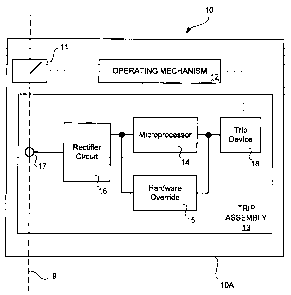
[0033] A block diagram in schematic form of a molded case circuit breaker 10
is
shown in Figure 3. The circuit breaker 10 includes a housing 10A in which a
number
of separable contacts 11 (e.g., a pair per each phase or power line) are
contained. As
shown in Figure 3, separable contacts 11 are associated with a conductor 9 of
a power
distribution system (only one phase of which is illustrated). The separable
contacts 11
may be operated automatically in response to an overcurrent condition. The
separable
contacts 11 may also be operated manually by way of a handle (not shown)
disposed
on the outside of the circuit breaker 10. Typically, such circuit breakers 10
include an
CA 02577561 2007-02-06
-7-
operating mechanism 12, which rapidly opens and closes the separable contacts
11,
and a trip assembly 13, which senses overcurrent conditions. Upon sensing an
overcurrent condition, the trip assembly 13 actuates the operating mechanism
12 to a
trip position which moves the separable contacts 11 to their open position.
[0034] In the current embodiment, trip assembly 13 employs both a
microprocessor
14 and a hardware override circuit 15 to detect an overcurrent condition
and/or to
actuate the operating mechanism 12. As shown in Figure 3, the trip assembly 13
includes a number of sensors such as, and without limitation, a current
transformer 17
which provides, to a rectifier circuit 16, a current proportional to the
current flowing
in conductor 9. The output of the rectifier circuit 16 is provided to both the
microprocessor 14 and the hardware override circuit 15. In response to an
overcurrent
condition, the microprocessor 14 and/or the hardware override circuit 15
produce
various trip signals (e.g., short delay trip; long delay trip; instantaneous
trip;
breakpoint trip; etc.) which are provided to a trip device 18. The trip device
18, in
turn, actuates the operating mechanism 12.
[0035] It should be noted that the particular arrangement of devices
illustrated in
Figure 3 is exemplary and other arrangements, within in the scope of the
invention,
are contemplated. For example, although discussed as separate components, it
is
contemplated that the hardware override circuit 15 and the microprocessor 14
may be
implemented as a single device, such as and without limitation, an integrated
circuit.
Also, one or more power lines or phases may be employed.
[0036] A schematic of the hardware override circuit 15 according to one
embodiment
of the present invention is illustrated in Figure 4. As discussed above in
conjunction
with Figure 3, the current transformer 17 produces a current in proportion to
the
current flowing through separable contacts 11. The output of the current
transformer
17 is supplied to bridge rectifier circuit 16. The current output of the
bridge rectifier
circuit 16 is provided to the hardware override circuit 15, where it develops
a negative
voltage across a burden resistor 19 with respect to the hardware override
circuit 15
common. If the magnitude of this negative voltage is large enough, diode 20
becomes
forward biased.
CA 02577561 2007-02-06
-8-
[0037] The hardware override circuit 15 employs an array 30 having zener diode
21,
zener diode 21 a, and resistor 22. In the exemplary embodiment, zener diode 21
is
electrically connected in parallel with the series combination of zener diode
21 a and
resistor 22. Furthermore, in the exemplary embodiment, the break over voltage
for
zener diode 21 is greater than the break over voltage of zener diode 21 a.
Accordingly, if the negative voltage developed at the burden resistor 19
reaches a first
predetermined value, diode 20 becomes forward biased and zener diode 21 a
breaks
over (i.e., the voltage exceeds the break voltage of the zener diode 21 a).
Referring
briefly to Figure 5, which shows an exemplary portion of a time-trip curve for
the
hardware override circuit 15 of Figure 4, diode 21 a breaks over at a current
factor of
about 15 to 20.
[0038] As a result of diode 21a breaking over, current flows through resistor
22
which, in conjunction with capacitor 23, delays generation of a trip signal
output by
comparator 24. As seen in Figure 5, the delay in this example is a time factor
of about
0.06. More specifically, resistor 22 and capacitor 23 provide an RC time
constant
which increases the amount of time that it takes for the voltage at the
inverting input
(-) of comparator 24 to drop below a reference voltage, Vref (applied at the
non-
inverting input (+) of comparator 24). Once the voltage at the inverting input
(-) of
comparator 24 drops below Vref, however, the output signal of the comparator
24,
which is provided to the trip device 18 (as shown in Figure 3), changes
states; thereby
initiating the trip of the circuit breaker 10.
[0039] If the negative voltage at burden resistor 19 reaches a second
predetermined
value, zener diode 21 breaks over (i.e., the voltage exceeds the break voltage
of the
zener diode 21). Referring briefly to Figure 5, diode 21 breaks over at a
current factor
of about 20 or greater. After breaking over, the zener diode 21 begins to
conduct
which, in turn, causes the voltage at the inverting input (-) of a comparator
24 to
immediately drop to a level which is less than reference voltage, Vref. As a
result, the
output signal of the comparator 24, which is provided to the trip device 18
(shown in
Figure 3), changes states thereby initiating the trip of the circuit breaker
10 (i.e.,
within a time factor of about 0.01).
CA 02577561 2007-02-06
-9-
[0040] It should be noted that the particular arrangement of devices
illustrated in
Figure 4 is exemplary and other arrangements, within in the scope of the
invention,
are contemplated. For example, diode 20 may be omitted from the hardware
override
circuit 15 while remaining within the scope of the present invention.
[0041 ] Referring to Figure 5, the portion of the time-trip curve between the
fixed time
short delay trip-curve function and the instantaneous trip-curve function is
referred to
herein as a "breakpoint trip-curve function". The components of the trip
assembly 13
(Figure 3) which provide a breakpoint trip may be referred to as a "breakpoint
trip
mechanism". In the embodiment illustrated in Figure 4, for example and without
limitation, zener diode 21 a, resistor 22, capacitor 23, and comparator 24 of
hardware
override circuit 15 form a breakpoint trip mechanism.
[0042] Additionally, the components of the trip assembly 13 which produce an
instantaneous trip may be referred to as an "instantaneous trip mechanism".
For
example, and without limitation, zener diode 21 and comparator 24 of hardware
override circuit 15 form an instantaneous trip mechanism. Furthermore, the
components of the trip assembly 13 which produce a short delay trip, may be
referred
to as a "short delay trip mechanism". For example, and without limitation,
processor
14 forms a short delay trip mechanism. Furthermore, the components of the trip
assembly 13 which produce a long delay trip may be referred to as a "long
delay trip
mechanism". For example, and without limitation, processor 14 forms a long
delay
trip mechanism. A number of components of trip assembly 13 may be structured
to
produce a trip signal (e.g., electrical and/or mechanical) for actuating the
operating
mechanism 12 in response to one or more of the short delay trip, the
breakpoint
trip(s), and/or the instantaneous trip. For example, and without limitation,
trip device
18 (Figure 3) is structured to produce this trip signal in the present
embodiment.
[0043] Although the instant embodiment is discussed in conjunction with a
short
delay trip-curve function and an instantaneous trip-curve function, it should
be
apparent that the breakpoint trip-curve function of the present invention may
be used
with any trip-curve functions, alone or in combination. For example, and
without
limitation, it is contemplated that a circuit breaker may employ a time-trip
curve
having, in addition to a breakpoint trip-curve portion, any one or more of a
long delay
CA 02577561 2007-02-06
- 10-
trip portion, a short delay trip portion, an instantaneous trip portion,
and/or a ground
fault trip portion. Furthermore, it is contemplated that one or more of these
trip-curve
functions may be implemented using various (e.g., thermal; magnetic;
instantaneous;
etc.) devices while remaining within the scope of the present invention.
[0044] Returning to Figure 4, it should be noted that the amount of delay
between
when zener diode 21 a breaks over and the output of comparator 24 changes
state is
selectable by changing the value of resistor 22 and/or the value of capacitor
23. For
example, a circuit breaker 10' (Figure 8) having a breakpoint trip-curve
function
(Figure 9) with a current factor of between about 15 and 20 and a time factor
of about
0.04 may be obtained by reducing the resistance of the resistor 22 and/or
reducing the
capacitance of capacitor 23. Likewise, a circuit breaker 10" (Figure 8) having
breakpoint trip-curve function (Figure 10) with a current factor of between
about 15
and 20 and a time factor of about 0.02 may be obtained by further reducing the
resistance of the resistor 22 and/or the capacitance of capacitor 23. As will
be
discussed below in conjunction with Figure 8, these circuit breakers (i.e.,
10, 10',
10"), each having different overcurrent/time trip characteristics, may be used
to
coordinate high current interruptions in a power distribution system.
[0045] It should further be noted that the time-trip curve may contain (and
the
hardware override circuit 15 structured to implement) more than one breakpoint
trip-
curve function. Figure 6, for example, is a schematic diagram of a hardware
override
circuit 15' for a circuit breaker (not shown) having more than one breakpoint
trip-
curve function (as shown in Figure 7) according to another embodiment of the
present
invention. Hardware override circuit 15' may be used, for example and without
limitation, to coordinate switching apparatus (not shown) in a power
distribution
system (not shown).
[0046] Hardware override circuit 15' has an array 30' having components which
form
portions of two breakpoint trip mechanisms. The first breakpoint trip
mechanism
includes, without limitation, zener diode 21 a', resistor 22', capacitor 23',
and
comparator 24'; the second breakpoint trip mechanism includes, without
limitation,
zener diode 21b, resistor 22a, capacitor 23', and comparator 24'. In this
embodiment,
zener diode 21' is electrically connected in parallel with the series
combination of
CA 02577561 2007-02-06
-11-
zener diode 21 a' and resistor 22', and in parallel with series combination of
zener
diode 21b and resistor 22a. Although shown with two breakpoint trip
mechanisms,
any number may be employed while remaining within the scope of the present
invention.
[0047] In the exemplary embodiment, the break over voltage for zener diode 21'
is
greater than the break over voltage of zener diode 21 a' which voltage, in
turn, is
greater than the break over voltage of zener diode 21 b. Additionally, the
resistance
value of resistor 22' is less than the resistance value of resistor 22a.
[0048] Accordingly, if the negative voltage at burden resistor 19' reaches a
first
predetermined value, diode 20' becomes forward biased and zener diode 21b
breaks
over (i.e., the voltage exceeds the break voltage of the zener diode 21b).
Referring
briefly to Figure 7, which is an exemplary portion of a time-trip curve for
the
hardware override circuit 15' as shown in Figure 6, diode 21 b breaks over at
a current
factor of about 15 to 20. As a result of diode 21 b breaking over, current
flows
through resistor 22a which, in conjunction with capacitor 23, delays the
voltage drop
at the inverting input of comparator 24' (and thus, delays generation of the
trip signal).
As seen in Figure 7, the delay in this example is a time factor of about 0.05.
Once the
voltage at the inverting input (-) of comparator 24' drops below Vref,
however, the
output signal of the comparator 24' changes states thereby initiating the trip
of the
circuit breaker (not shown).
[0049] If the negative voltage at burden resistor 19' reaches a second
predetermined
value, zener diode 21a' breaks over (i.e., the voltage exceeds the break
voltage of the
zener diode 21 a'). Referring briefly to Figure 7, diode 21 a' breaks over at
a current
factor of about 20 to 25. As a result of diode 21 a' breaking over, current
flows
through resistor 22' which, in conjunction with capacitor 23', delays
generation of a
trip signal. As discussed above, resistor 22' has a resistance value that is
less than the
resistance value of resistor 22a. Thus, as seen in Figure 7, the delay caused
by
resistor 22' and capacitor 23' (a time factor of about 0.03 in this example)
is less than
the delay caused by resistor 22a and capacitor 23'. Once the voltage at the
inverting
input (-) of comparator 24' does drop below Vref, however, the output signal
of the
comparator 24' changes states thereby initiating the trip of the circuit
breaker.
CA 02577561 2007-02-06
- 12-
[0050] If the negative voltage at burden resistor 19' reaches a third
predetermined
value, zener diode 21' breaks over (i.e., the voltage exceeds the break
voltage of the
zener diode 21'). Referring briefly to Figure 7, diode 21' breaks over at a
current
factor of about 25 or greater. After breaking over, the zener diode 21' begins
to
conduct which, in turn, causes the voltage at the inverting input (-) of a
comparator
24' to immediately drop to a level which is less than a reference voltage,
Vref. As a
result, the output signal of the comparator 24' changes states thereby
initiating the trip
of the circuit breaker (i.e., within a time factor of about 0.01).
[0051 ] It should be noted that the particular arrangement of devices
illustrated in
Figure 6 is exemplary and other arrangements, within in the scope of the
invention,
are contemplated. For example, diode 20' may be omitted from the hardware
override
circuit 15' while remaining within the scope of the present invention
[0052] Figure 8 illustrates a typical electric power distribution system 25
having a bus
26 which provides power to a number of other buses 27a, 27b which, in turn,
energize
a number of other buses 28a - 28e. For clarity, and without limitation, the
bus 26 is
referred to herein as the "main bus"; the buses 27a - 27b are referred to as
"intermediate buses"; and the buses 28a - 28e are referred to as "distribution
circuits".
[0053] Distribution circuits 28a - 28e provide power to a number of load
devices 29a
- 29e. Often, power transformers (not shown) step down the voltage at various
points
in the distribution system 25. An electrical switching apparatus is provided
for the
main bus 26 (i.e., circuit breaker 10), for at least some, if not all, of the
intermediate
busses 27a - 27b (i.e., circuit breakers 10'), and for at least some, if not
all, of the
distribution circuits 28a - 28e (i.e., circuit breakers 10").
[0054] Depending upon their location within the distribution system 25, an
electrical
switching apparatus may be referred to as being "upstream" and/or "downstream"
of
another electrical switching apparatus. For example, the circuit breaker 10'
associated
with intermediate bus 27a is both downstream of circuit breaker 10 for main
bus 26
and upstream of the circuit breakers 10" associated with distribution circuits
29a -
29c.
CA 02577561 2007-02-06
-13-
[0055] Each circuit breaker 10, 10', 10" has its own overcurrent/time trip
characteristic for responding to faults in the distribution system 25. These
overcurrent/time trip characteristics are coordinated through a hierarchical
arrangement in order that only the closest protection device above the fault
trips to
minimize the interruption to service in the distribution system 25.
[0056] As discussed above, circuit breaker 10 has a breakpoint trip-curve
function
(Figure 5) with a current factor of between about 15 and 20 and a time factor
of about
0.06; circuit breaker 10' has a breakpoint trip-curve function (Figure 9) with
a current
factor of between about 15 and 20 and a time factor of about 0.04; and circuit
breaker
10" has a breakpoint trip-curve function (Figure 10) with a current factor of
between
about 15 and 20 and a time factor of about 0.02. Figure 11 illustrates the
time-trip
curve of circuit breaker 10 (Figure 5), the time-trip curve of circuit breaker
10'
(Figure 9), and the time-trip curve of circuit breaker 10" (Figure 10)
superimposed on
a single graph.
[0057] Referring to Figure 8, should load 29a develop a high current fault,
for
example, it is desirable to trip only the circuit breaker 10" associated with
distribution
circuit 28a (to which load 29a is electrically connected) without tripping the
circuit
breaker 10' associated with intermediate bus 27a and/or circuit breaker 10
associated
with main bus 26. For instance, should the fault at load 29a have a current
factor of
18, circuit breaker 10" will trip within a time factor of 0.02. This affords
circuit
breaker 10" the opportunity to clear the fault associated with load 29a
without circuit
breaker 10' and/or circuit breaker 10 (which have time factors of 0.04 and
0.06,
respectively) tripping. By only tripping the circuit breaker 10" associated
with
distribution circuit 28a, the power supplied to the other branches (e.g.,
distribution
circuits 28b - 28c) fed by the bus 27a, as well as the power supplied to the
intermediate bus 27b fed by the main bus 26, remain uninterrupted. Although
not
shown, power distribution system 25 may employ a number of circuit breakers at
least
one of which has a plurality of breakpoint trip mechanisms.
[0058] Additionally, the power distribution system 25 may employ a number of
circuit breakers which have the same breakpoint delay time factors, but
different pick-
up current factors. Figure 12, for example, illustrates the time-trip curves
of three
CA 02577561 2007-02-06
-14-
circuit breakers (10a, 10b, lOc) superimposed on a single graph. As shown in
Figure
12, each of these circuit breakers (10a, l Ob, 1 Oc) have a breakpoint delay
time factor
of approximately 0.01, however, circuit breaker lOc picks-up at a current
factor of
between about 12 and 17, circuit breaker l Ob picks-up at a current factor of
between
about 17 and 22, and circuit breaker l0a picks-up at a current factor of
between about
22 and 30.
[0059] Further the power distribution system 25 may employ a number of circuit
breakers which have the different breakpoint delay time factors and different
pick-up
current factors. Figure 13, for example, illustrates the time-trip curves of
three circuit
breakers (l0a', lOb', lOc') superimposed on a single graph. As shown in Figure
13,
circuit breaker l Oc' has a breakpoint delay time factor of approximately 0.02
and
picks-up at a current factor of between about 12 and 17, circuit breaker l Ob'
has a
breakpoint delay time factor of approximately 0.04 and picks-up at a current
factor of
between about 17 and 22, and circuit breaker l0a' has a breakpoint delay time
factor
of approximately 0.06 and picks-up at a current factor of between about 22 and
30.
[0060] While specific embodiments of the invention have been described in
detail, it
will be appreciated by those skilled in the art that various modifications and
alternatives to those details could be developed in light of the overall
teachings of the
disclosure. Accordingly, the particular arrangements disclosed are meant to be
illustrative only and not limiting as to the scope of the invention which is
to be given
the full breadth of the claims appended and any and all equivalents thereof.
CA 02577561 2007-02-06
REFERENCE CHARACTER LIST
hardware override circuit 1
current transformer 2
separable contacts 3
bridge rectifier circuit 4
burden resistor 5
diode 6
zener diode 7
comparator 8
electric conductor 9
circuit breaker 10, 10', 10"
housing 10A
separable contacts 11
operating mechanism 12
trip assembly 13
microprocessor 14
hardware override circuit 15, 15'
rectifier circuit 16
current transformer 17
trip device 18
burden resistor 19, 19'
diode 20, 20'
zener diode 21, 21a, 21b, 21a'
resistor 22, 22a, 22'
capacitor 23, 23'
comparator 24, 24'
power distribution system 25
main bus 26
intermediate bus 27a - 27b
distribution circuits 28a - 28e
load devices 29a - 29e
array 30, 30'