Note: Descriptions are shown in the official language in which they were submitted.
CA 02578060 2007-02-26
- 1 -
SPECIFICATION
SEMICONDUCTOR TEST SYSTEM
[Technical Field]
The present invention relates to a semiconductor
test system. Particularly, the present invention is
suitably applied to a test system for testing
electric characteristics of a super multi-pin output
LSI.
[Background Art]
In display apparatuses, such as liquid crystal
displays, organic EL displays, plasma displays and
field emission displays, image data are processed in
an electronic circuit, such as a drive circuit, and
outputted from a plurality of output terminals of the
drive circuit to display elements. Since the electric
characteristics of drive transistors disposed
corresponding to the output terminals of the drive
circuit and components of the electronic circuit vary
to no small extent, the signal values outputted from
the output terminals vary accordingly. Therefore, it
is necessary to provide a test apparatus (test
system) that measures relative errors and absolute
CA 02578060 2007-02-26
- 2 -
errors of the signal values outputted from the output
terminals to sort out defective products.
Figure 1 is a simplified diagrammatic view
showing a conventional test system for testing an LSI
formed on a wafer W. As shown in Figure 1, the
conventional test system includes a workstation 100,
a tester body 101, a test head 102, a performance
board 103, a probe card 104 and a prober 105. The
probe card 104 has a plurality of probe needles 104a
disposed thereon.
The wafer W to be tested is placed on a chuck
(not shown) formed on the prober 105, and the probe
needles 104a of the probe card 104 are moved to touch
input/output terminals of the LSI formed on the wafer
W. The probe card 104 is connected to the test head
102 via the performance board 103, and the test head
102 is connected to the tester body 101 via a cable
106.
The test head 102 performs preprocessing, such as
amplifying the signal outputted from each of the
output terminals of the LSI and inputted via the
probe card 104 and the performance board 103 and
converting the inputted signal into digital data. The
preprocessing is carried out by a front-end card
removably attached to the test head 102. The tester
CA 02578060 2007-02-26
- 3 -
body 101 performs pass/fail judgment of the LSI
formed on the wafer W according to a test program
stored therein and based on the characteristic
measurement data sent via the test head 102.
Postprocessing including the pass/fail judgment is
carried out by a module removably attached to the
tester body 101.
The performance board 103 is electrically
connected to the test head 102 and the probe card 104
in a removable manner. By exchanging the module in
the tester body 101, the front-end card in the test
head 102 and the performance board 103 according to
the LSI to be tested, LSIs designed in different
standards can be handled in a flexible manner.
A test of a semiconductor circuit that outputs
image signals from a large number of pins (a
representative example of this is a drive LSI for a
display apparatus) involves a large number of output
values to be measured. To improve the throughput, it
is necessary to perform parallel processing, such as
simultaneous measurement of the output values. To
this end, there has been conventionally provided a
multi-pin test system in which the number of the
probe needles 104a disposed on the probe card 104
CA 02578060 2007-02-26
- 4 -
corresponds to the number of output terminals (pins)
of the drive LSI.
However, recent drive LSIs have been designed in
an increasingly dense manner, so that it is necessary
to dispose more than 1000 probe needles (pins) 104a
on the probe card 104. When the number of pins is
1000, signals corresponding to 1000 pins are handled
in parallel among the tester body 101, the test head
102, the performance board 103 and the probe card 104.
Thus, such a multi-pin test system has a
significantly large-scale configuration.
To eliminate such inconvenience, there has been
proposed a technology in which signals outputted from
a plurality of output terminals of a drive LSI are
separately outputted to the outside from test
terminals provided at the rate of one for every
predetermined number of the output terminals (see
Japanese Patent No. 3199827, for example).
According to Japanese Patent No. 3199827,
switches are disposed between each of the test
terminals and the predetermined number of output
terminals, and the switch successively and
selectively outputs the image signal delivered to the
output terminal to the test terminal. In such
configuration, the test can be performed by using the
CA 02578060 2007-02-26
- 5 -
image signals outputted from the test terminals whose
number is smaller than the large number of output
terminals. It is accordingly possible to handle super
multi-pin drive LSIs.
However, when the technology described in
Japanese Patent No. 3199827 is used, the image
signals delivered to the large number of output
terminals are successively outputted via the test
terminals. This requires longer test time than
simultaneously measuring all output values,
disadvantageously resulting in corresponding
increased test cost. Furthermore, when the technology
described in Japanese Patent No. 3199827 is used, the
output signal from the test terminal is an analog
signal, so that noise components are easily
superimposed on the output signal and it is hence
difficult to perform highly accurate testing.
[Disclosure of the Invention]
The present invention has been made to solve such
problems and aims to provide a small-scale test
system capable of testing electric characteristics of
a super multi-pin output LSI in a quick and highly
accurate manner.
CA 02578060 2007-02-26
- 6 -
To solve the above problems, the semiconductor
test system according to the present invention
multiplexes a plurality of analog signals outputted
from a plurality of output terminals of a
semiconductor to be tested in an early stage to
reduce the number of signals, performs A/D conversion,
averaging and calibration on the resultant
multiplexed signal and supplies the calibrated
characteristic measurement data to a semiconductor
pass/fail judgment section.
According to the thus configured present
invention, since the plurality of analog signals
outputted from the plurality of output terminals are
multiplexed to reduce the number of signals in an
early stage and data are averaged in an early stage
after the A/D conversion to reduce the amount of data,
a large number of parallel transportation paths and
processing circuits are not required, allowing
reduction in the size of the apparatus. Furthermore,
the number of signals and the amount of data are thus
reduced, allowing improved throughput, faster
processing and significant reduction in test time.
Moreover, since data sampled multiple times are
averaged and calibrated for the following pass/fail
judgment, the effects of random noise and systematic
CA 02578060 2007-02-26
- 7 -
noise superimposed on the data are reduced, allowing
high accuracy testing. By using a high operation
speed multiplexer and A/D converter, the number of
sampling in a short period of time can be increased
for averaging, allowing higher testing accuracy.
In another aspect of the present invention, a
primary pass/fail judgment is performed based on
characteristic measurement digital data obtained by
A/D converting a plurality of analog signals
outputted from a plurality of analog output terminals
of a semiconductor. Then, secondary pass/fail
judgment is performed based on the digital data that
have passed the primary pass/fail judgment.
According to the thus configured present
invention, the following advantages are provided in
addition to those described above. That is, according
to the present invention, only digital data that have
passed the primary pass/fail judgment undergo the
secondary pass/fail judgment. This reduces the amount
of digital data to be sent to the secondary judgment
processor, allowing improved throughput, faster
processing and significant reduction in test time.
In another aspect of the present invention,
digital signals outputted from a plurality of output
terminals of a semiconductor to be tested are T/D
CA 02578060 2007-02-26
- 8 -
converted, averaged and calibrated, and the
calibrated characteristic measurement data are
supplied to a semiconductor pass/fail judgment
section.
According to the thus configured present
invention, since the digital signals outputted from
the plurality of output terminals are T/D converted
and averaged in an early stage after the T/D
conversion to reduce the amount of data, a large
number of parallel transportation paths and
processing circuits are not required, allowing
reduction in the size of the apparatus. Furthermore,
the reduced amount of data allows improved throughput,
faster processing and significant reduction in test
time. Moreover, since data sampled multiple times are
averaged and calibrated for the following pass/fail
judgment, the effects of random noise and systematic
noise superimposed on the data are reduced, allowing
high accuracy testing.
[Brief Description of the Drawings]
Figure 1 shows a simplified configuration of a
conventional test system for testing an LSI formed on
a wafer;
CA 02578060 2007-02-26
- 9 -
Figure 2 shows an exemplary schematic
configuration of the entire test system according to
first to fifth embodiments;
Figure 3 is a block diagram showing an exemplary
inner configuration of the mother board and the
daughter board according to the first embodiment;
Figure 4 is a block diagram showing an exemplary
schematic configuration of the multiplexer according
to the first, second and fifth embodiments;
Figure 5 is a block diagram showing an exemplary
inner configuration of the mother board and the
daughter board according to the second embodiment;
Figure 6 is a block diagram showing an exemplary
inner configuration of the mother board and the
daughter board according to the third embodiment;
Figure 7 is a block diagram showing an exemplary
inner configuration of the mother board and the
daughter board according to the fourth embodiment;
and
Figure 8 is a block diagram showing an exemplary
inner configuration of the mother board and the
daughter board according to the fifth embodiment.
[Best Mode for Carrying Out the Invention]
(First Embodiment)
CA 02578060 2007-02-26
- 10 -
A first embodiment according to the present
invention will be described below with reference to
the drawings. Figure 2 shows an exemplary schematic
configuration of the entire test system according to
the first embodiment. As shown in Figure 2, the test
system according to the first embodiment includes a
personal computer 10, a mother board 11, a daughter
board 12, a probe card 13, a chuck 14 and a prober 15.
The probe card 13 has a plurality of probe needles
13a disposed thereon.
The wafer W to be tested is placed on the chuck
14 formed on the prober 15, and the probe needles 13a
of the probe card 13 are moved to touch input/output
terminals of an LSI formed on the wafer W. The probe
card 13 is connected to the mother board 11 via the
daughter board 12, and the mother board 11 is
connected to the personal computer 10 via an I/0
cable 16. Although the mother board 11 is directly
connected to the personal computer 10 by the I/0
cable 16 in this embodiment, the connection may be
achieved via a network, such as the Internet or a LAN
(Local Area Network).
The daughter board 12 is electrically connected
to the mother board 11 and the probe card 13 in a
removable manner. By exchanging the daughter board 12
CA 02578060 2007-02-26
- 11 -
according to the LSI to be tested, LSIs designed in
different standards can be handled in a flexible
manner.
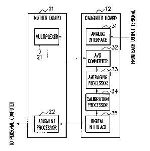
Figure 3 is a block diagram showing an exemplary
inner configuration of the mother board 11 and the
daughter board 12. As shown in Figure 3, the mother
board 11 includes a multiplexer 21 and a judgment
processor 22. The daughter board 12 includes an
analog interface 31, an A/D (Analog/Digital)
converter 32, an averaging processor 33, a
calibration processor 34 and a digital interface 35.
The analog interface 31 on the daughter board 12
receives a plurality of analog signals outputted from
a plurality of analog output terminals of the LSI
formed on the wafer W via the probe card 13 and
outputs them to the multiplexer 21 on the mother
board 11. The inputted analog signals are voltage
values outputted from the plurality of analog output
terminals through an inner circuit of the LSI when
test data are inputted to the LSI being tested.
The multiplexer 21 multiplexes the plurality of
analog signals inputted from the analog interface 31
to reduce the number of signals and supplies the
resultant signals to the A/D converter 32 on the
daughter board 12. The A/D converter 32 converts the
CA 02578060 2007-02-26
- 12 -
analog signals returned from the multiplexer 21 on
the mother board 11 into digital data.
The averaging processor 33 averages digital data
(digitized voltage values) sampled multiple times by
the A/D converter 32. The averaging can reduce random
errors of the voltage values resulting from the noise
generated in the LSI being tested. Averaging in an
early stage after the A/D conversion reduces the
amount of data, making the following processing
easier.
The calibration processor 34 reduces systematic
errors generated in the LSI (the noise that is not
random but having a certain tendency). For example,
the calibration processor 34 subtracts a
predetermined offset value from the digital data
value outputted from the averaging processor 33. The
offset value to be set in this case is an appropriate
value as the amount of shift from the expectation
value of the voltage to be outputted from the output
terminal upon the input of the test data to the LSI.
The digital interface 35 receives the digital
data calibrated by the calibration processor 34 and
outputs it to the mother board 11. The judgment
processor 22 on the mother board 11 performs
pass/fail judgment on the LSI being tested based on
CA 02578060 2007-02-26
- 13 -
the digital data inputted from the digital interface
35 and outputs the result to the personal computer 10
via the I/O cable 16.
As shown in Figure 4, the multiplexer 21 has a
plurality of transistor switches 41 connected in a
tournament manner. The plurality of analog signals
outputted from the plurality of analog output
terminals of the LSI via the probe card 13
successively pass through the plurality of transistor
switches 41 so that the analog signals are
multiplexed, allowing reduction in the number of
signals. For example, when the LSI being tested has
1000-pin outputs (for example, source: 720 pins,
gate: 320 pins), the 1000 analog signals outputted
from the 1000 pins are multiplexed into one source
analog signal and one gate analog signal.
In general, when a plurality of transistor
switches are connected in a tournament manner, a
transistor switch at a later stage also receives the
load on a plurality of preceding transistor switches.
Therefore, the later the transistor switch is
disposed, the larger the amount of load on the
transistor switch is. When a large number of
transistor switches are connected in a tournament
manner, the large load thus generated causes
CA 02578060 2007-02-26
- 14 -
reduction in the operation speed of the multiplexer
21. In this embodiment, relay switches are provided
at several locations where the transistor switches
are disposed and these relay switches are turned on
and off. When one of the relay switches is turned off,
the load on the transistor switch connected to the
preceding stage can be separated to reduce the amount
of load on the transistor switch connected to the
subsequent stage. This increases the operation speed
of the multiplexer 21. In this embodiment, the
multiplexing operation for 1000-pin outputs can be
completed in a period of time as short as about 1 ms.
As the A/D converter 32 that A/D converts the
analog signal multiplexed at high speed, a high-speed
A/D converter operating at a speed comparable to that
of the multiplexer 21, which is 100 ns, is used. The
A/D converter 32 to be employed has a conversion
accuracy of 12 bits, for example. Thus, while each of
the 1000 analog signals outputted from the plurality
of analog output terminals of the LSI being tested
are sampled ten times for averaging, the averaged
signal can be converted into 12-bit accuracy digital
data in a period of time as short as about 1 ms.
In this embodiment, the analog signals outputted
from each of the output terminals after inputting the
CA 02578060 2007-02-26
- 15 -
same test data to the LSI are sampled, for example,
ten times by the A/D converter 32 and the results are
averaged by the averaging processor 33. The averaging
reduces the effect of noise superimposed on each of
the analog signals, so that highly accurate
characteristic measurement data can be acquired. As
described above, sampling 1000-pin analog signals
once requires only about 100 s. Characteristic
measurement data is then obtained by averaging the
digital data sampled ten times, so that the measuring
time will be about 1 ms in total. This is a
significantly short period of time compared to about
1 second conventionally required for one test,
allowing significant reduction in test time compared
to that conventionally required.
That is, conventionally, the tester body 101 is
connected to the test head 102 by the dedicated cable
106 as shown in Figure 1, and a large amount of data
is sent via the dedicated cable 106 for data
processing in the tester body 101. Thus, not only
does the limitation of the transfer speed through the
dedicated cable 106 affects the test time but also
the pass/fail judgment of the LSI needs to use the
large amount of data sent to the tester body 101, so
that a large amount of time is required for one test.
CA 02578060 2007-02-26
- 16 -
In contrast, in this embodiment, wiring is only
used on the substrates, that is, the mother board 11
and the daughter board 12, and the high-speed
multiplexer 21 and the high-speed A/D converter 32
are used. This allows multiplexing and A/D conversion
to be performed in a period of time as short as about
100 ns, so that the processing frequency can be
increased to about 10 MHz. Even when sampling is
performed ten times for averaging in order to
increase the accuracy of measured data, total
processing time is significantly short, which is only
about 1 ms. Furthermore, the number of signals
outputted from the daughter board 12 to the judgment
processor 22 on the mother board 11 is significantly
reduced by the multiplexing process in the early
stage and the amount of data is reduced by the
averaging process in the averaging processor 33 in
the relatively early stage after the A/D conversion,
allowing the throughput to be improved.
As described above in detail, according to the
first embodiment, the test for electric
characteristics of a super multi-pin output LSI (such
as a gate driver test and a source driver test for
measuring driver voltages) can be carried out in a
quick and highly accurate manner. Furthermore, since
CA 02578060 2007-02-26
- 17 -
the plurality of analog signals outputted from the
plurality of output terminals of the LSI are
multiplexed in the early stage to reduce the number
of signals and the digital data are averaged in the
early stage after the A/D conversion to reduce the
amount of data, a large number of parallel
transportation paths and processing circuits are not
required, allowing significant reduction in the scale
of the configuration of the test system compared to
that conventionally required.
(Second Embodiment)
A second embodiment of the present invention will
be described below with reference to the drawings.
The whole configuration of the test system according
to the second embodiment is the same as that shown in
Figure 2.
Figure 5 is a block diagram showing an exemplary
inner configuration of the mother board 11 and the
daughter board 12 according to the second embodiment.
In Figure 5, since the components having the same
reference characters as those shown in Figure 3 have
the same functions, redundant description thereof
will be omitted.
As shown in Figure 5, the mother board 11
according to the second embodiment includes a
CA 02578060 2007-02-26
- 18 -
secondary judgment processor 23 instead of the
judgment processor 22 shown in Figure 3. The daughter
board 12 according to the second embodiment further
includes a primary judgment processor 36 between the
calibration processor 34 and the digital interface 35.
The primary judgment processor 36 performs
primary pass/fail judgment on the digital data
calibrated by the calibration processor 34 to
eliminate unnecessary data. In this process, for
example, when the calibration processor 34 subtracts
a predetermined offset value from the digital data
value and the resultant computed data value still
significantly differs from the expectation value (for
example, when the difference between the data value
outputted from the calibration processor 34 and the
expectation value is equal to or greater than a
predetermined value), the primary judgment processor
36 judges that the LSI being tested is defective and
discards the data.
In the second embodiment, the digital interface
35 outputs only digital data judged to be passed in
the primary pass/fail judgment performed in the
primary judgment processor 36 to the mother board 11.
The secondary judgment processor 23 on the mother
board 11 performs secondary pass/fail judgment on the
CA 02578060 2007-02-26
- 19 -
LSI being tested based on the digital data inputted
from the digital interface 35 and outputs the result
to the personal computer 10 via the I/0 cable 16. The
secondary pass/fail judgment performed in the
secondary judgment processor 23 is similar to the
pass/fail judgment performed in the judgment
processor 22 shown in Figure 3 and a more advanced
process than the primary pass/fail judgment performed
in the primary judgment processor 36. Therefore, the
pass/fail judgment performed in the secondary
judgment processor 23 takes longer than the pass/fail
judgment performed in the primary judgment processor
36.
As described above in detail, in the second
embodiment, by performing the simple pass/fail
judgment before the advanced pass/fail judgment is
performed, LSIs being tested and apparently
considered to be defective will not undergo further
testing. That is, only digital data that have passed
the primary pass/fail judgment performed in the
primary judgment processor 36 are sent to the
secondary judgment processor 23 for the secondary
pass/fail judgment, so that it is possible to reduce
the amount of digital data to be sent to the
secondary judgment processor 23 where testing takes a
CA 02578060 2007-02-26
- 20 -
longer period of time. This allows further improved
throughput, faster processing and significant
reduction in test time, compared to the first
embodiment described above.
(Third Embodiment)
A third embodiment of the present invention will
be described below with reference to the drawings. In
the first and second embodiments described above, the
voltage values outputted from the analog output
terminals after test data are inputted to the LSI to
be tested are used as reference values to test the
LSI. In contrast, in the third embodiment that will
be described below, temporal shifts (such as response
time) of digital data outputted from digital output
terminals after pulse-like digital data are inputted
to the LSI are used as reference values to test the
LSI (so-called timing test).
The whole configuration of the test system
according to the third embodiment is the same as that
shown in Figure 2. Figure 6 is a block diagram
showing an exemplary inner configuration of the
mother board 11 and the daughter board 12 according
to the third embodiment.
As shown in Figure 6, the mother board 11
according to the third embodiment includes a timing
CA 02578060 2007-02-26
- 21 -
generator 41, a switch array 42 and a judgment
processor 43. The daughter board 12 according to the
third embodiment includes a digital interface 51, a
T/D (Time/Digital) converter 52, an averaging
processor 53 and a calibration processor 54.
The timing generator 41 on the mother board 11
generates digital input signals (for example, pulse
signals, each having a rising edge and a falling edge
at a predetermined timing) supplied to the LSI being
tested and outputs them to the digital interface 51
on the daughter board 12. The digital interface 51
outputs the digital input signals supplied from the
timing generator 41 to the digital input terminals of
the LSI and receives resultant digital output signals
(characteristic measurement data of the LSI) returned
from the digital output terminals of the LSI. Then,
the digital data inputted from the LSI are outputted
to the switch array 42 on the mother board 11.
The switch array 42 switches multiple pieces of
digital data inputted from the digital interface 51
and supplies them to the T/D converter 52 on the
daughter board 12. In this embodiment, the
multiplexer is replaced with the switch array 42. The
reason for this is that the number of the digital
output terminals is not so large that the switch.
CA 02578060 2007-02-26
- 22 -
array 42 having an array of relay switches has enough
ability to handle the multiple pieces of digital data.
When the number of the digital output terminals is so
large that the number of the digital data values to
be inputted to the digital interface 51 is enormous,
the switch array 42 may be replaced with a
multiplexer. In this case, the multiplexer may be
configured by combining transistor switches and relay
switches, as in the multiplexer 21 shown in Figure 3.
When the switch array 42 is used, transistor switches
are not connected in a tournament manner as in a
multiplexer, so that a large load will not be applied,
allowing a high speed operation.
The T/D converter 52 performs analog-to-digital
conversion of the period of time spent from the time
when the digital data are inputted from the digital
interface 51 to the digital input terminals of the
LSI to the time when the digital data are outputted
from the digital output terminals of the LSI and
inputted to the T/D converter 52 via the switch array
42 (the response time spent from the time when the
pulse is inputted to the LSI to the time when
resultant measured data is obtained).
The averaging processor 53 averages multiple
pieces of digital data (digitized response time)
CA 02578060 2007-02-26
- 23 -
obtained from the T/D converter 52. For example,
digital signals outputted from the digital output
terminals after the same pulse data are inputted to
the LSI are used to digitize, for example, ten pieces
of response time data in the T/D converter 52 and the
results are averaged by the averaging processor 53.
The averaging can reduce random errors of the
response time data resulting from the noise generated
in the LSI being tested. Averaging in an early stage
reduces the amount of data, making the following
processing easier.
The calibration processor 54 reduces systematic
errors generated in the LSI being tested. For example,
the calibration processor 54 subtracts a
predetermined offset value from the digital data
value corresponding to the response time outputted
from the averaging processor 53. The offset value to
be set in this case is an appropriate value as the
amount of shift from the expectation value of the
response time spent from the time when the digital
data is inputted to the LSI to the time when
resultant measured data is obtained. The digital data
calibrated by the calibration processor 54 is
supplied to the judgment processor 43 on the daughter
board 12 via the digital interface 51.
CA 02578060 2007-02-26
- 24 -
The judgment processor 43 performs pass/fail
judgment of the LSI being tested based on the digital
data inputted from the digital interface 51 and
outputs the result to the personal computer 10 via
the I/0 cable 16.
In the thus configured third embodiment, wiring
is only used on the substrates, that is, the mother
board 11 and the daughter board 12. The amount of
data is reduced by the averaging process in the
averaging processor 53 in the relatively early stage
after the T/D conversion, allowing the throughput to
be improved.
Therefore, it is possible to perform electric
characteristic testing on a super multi-pin output
LSI (timing test to investigate the response time and
the like) in a quick and highly accurate manner.
Furthermore, since the digital data are averaged in
the early stage after the T/D conversion to reduce
the amount of data, a large number of parallel
transportation paths and processing circuits are not
required, allowing significant reduction in the scale
of the configuration of the test system compared to
that conventionally required.
CA 02578060 2007-02-26
- 25 -
(Fourth Embodiment)
A fourth embodiment of the present invention will
be described below with reference to the drawings.
The whole configuration of the test system according
to the fourth embodiment is the same as that shown in
Figure 2.
Figure 7 is a block diagram showing an exemplary
inner configuration of the mother board 11 and the
daughter board 12 according to the fourth embodiment.
In Figure 7, components having the same reference
characters as those shown in Figure 6 have the same
functions and redundant description thereof will be
omitted.
As shown in Figure 7, the mother board 11
according to the fourth embodiment includes a
secondary judgment processor 44 instead of the
judgment processor 43 shown in Figure 6. The daughter
board 12 according to the second embodiment further
includes a primary judgment processor 55 between the
calibration processor 54 and the digital interface 51.
The primary judgment processor 55 performs
primary pass/fail judgment on the digital data
calibrated by the calibration processor 54 to
eliminate unnecessary data. In this process, for
example, when the calibration processor 54 subtracts
CA 02578060 2007-02-26
- 26 -
a predetermined offset value from the digital data
value and the resultant computed data value still
significantly differs from the expectation value (for
example, when the difference between the data value
outputted from the calibration processor 54 and the
expectation value is equal to or greater than a
predetermined value), the primary judgment processor
55 judges that the LSI being tested is defective and
discards the data.
In the fourth embodiment, the digital interface
51 outputs only digital data judged to be passed in
the primary pass/fail judgment performed in the
primary judgment processor 55 to the mother board 11.
The secondary judgment processor 44 on the mother
board 11 performs secondary pass/fail judgment on the
LSI being tested based on the digital data inputted
from the digital interface 51 and outputs the result
to the personal computer 10 via the I/0 cable 16. The
secondary pass/fail judgment performed in the
secondary judgment processor 44 is similar to the
pass/fail judgment performed in the judgment
processor 43 shown in Figure 6 and a more advanced
process than the primary pass/fail judgment performed
in the primary judgment processor 55. Therefore, the
pass/fail judgment performed in the secondary
CA 02578060 2007-02-26
- 27 -
judgment processor 44 takes longer than the pass/fail
judgment performed in the primary judgment processor
55.
As described above in detail, in the fourth
embodiment, by performing the simple pass/fail
judgment before the advanced pass/fail judgment is
performed, LSIs being tested and apparently
considered to be defective will not undergo further
testing. That is, only digital data that have passed
the primary pass/fail judgment performed in the
primary judgment processor 55 are sent to the
secondary judgment processor 44 for the secondary
pass/fail judgment, so that it is possible to reduce
the amount of digital data to be sent to the
secondary judgment processor 44 where testing takes a
longer period of time. This allows further improved
throughput, faster processing and significant
reduction in test time, compared to the third
embodiment described above.
(Fifth Embodiment)
A fifth embodiment of the present invention will
be described below with reference to the drawings.
The fifth embodiment is a combination of the second
and fourth embodiments. The whole configuration of
CA 02578060 2007-02-26
- 28 -
the test system according to the fifth embodiment is
the same as that shown in Figure 2.
Figure 8 is a block diagram showing an exemplary
inner configuration of the mother board 11 and the
daughter board 12 according to the fifth embodiment.
In Figure 8, components having the same reference
characters as those shown in Figures 5 and 7 have the
same functions and redundant description thereof will
be omitted.
As shown in Figure 8, the mother board 11
according to the fifth embodiment includes the
multiplexer 21, the timing generator 41, the switch
array 42 and a secondary judgment processor 61. The
daughter board 12 according to the fifth embodiment
includes the analog interface 31, the A/D converter
32, the T/D converter 52, an averaging processor 71,
a calibration processor 72, a primary judgment
processor 73 and a digital interface 74.
The averaging processor 71 on the daughter board
12 has both functions of the averaging processor 33
shown in Figure 5 and the averaging processor 53
shown in Figure 7. That is, the averaging processor
71 averages digital data sampled multiple times by
the A/D converter 32 (digitized voltage values
obtained by inputting the test data to the LSI, which
CA 02578060 2007-02-26
- 29 -
corresponds to first digital data of the present
invention). The averaging processor 71 also averages
multiple pieces of digital data obtained from the T/D
converter 52 (digitized response time spent from the
time when the pulse is inputted to the LSI to the
time when resultant measured data is obtained, which
corresponds to second digital data of the present
invention).
The calibration processor 72 has both functions
of the calibration processor 34 shown in Figure 5 and
the calibration processor 54 shown in Figure 7. That
is, the calibration processor 72 subtracts
predetermined offset values from the digital data
values outputted from the averaging processor 71. The
offset values to be set in this case are appropriate
values as the amount of shift from the expectation
value of the voltage to be outputted from the output
terminal upon the input of the test data to the LSI
and the amount of shift from the expectation value of
the response time spent from the time when the pulse
is inputted to the LSI to the time when resultant
measured data is obtained.
The primary judgment processor 73 has both
functions of the primary judgment processor 36 shown
in Figure 5 and the primary judgment processor 55
CA 02578060 2007-02-26
- 30 -
shown in Figure 7 and eliminates unnecessary data
from the digital data calibrated by the calibration
processor 72. That is, when the calibration processor
36 subtracts a first offset value for a voltage value
from the first digital data value and the resultant
computed data value still significantly differs from
the expectation value, the primary judgment processor
73 judges that the LSI being tested is defective and
discards the data. Furthermore, when the calibration
processor 54 subtracts a second offset value for
response time from the second digital data value and
the resultant computed data value still significantly
differs from the expectation value, the primary
judgment processor 73 judges that the LSI being
tested is defective and discards the data.
The digital interface 74 outputs only digital
data judged to be passed in the primary pass/fail
judgment performed in the primary judgment processor
73 to the mother board 11.
The secondary judgment processor 61 on the mother
board 11 performs secondary pass/fail judgment on the
LSI being tested based on the digital data inputted
from the digital interface 74 and outputs the result
to the personal computer 10 via the I/0 cable 16. The
secondary judgment processor 61 performs
CA 02578060 2007-02-26
- 31 -
comprehensive judgment on the first digital data
(digitized voltage values) outputted from the analog
output terminals of the LSI, A/D converted and
supplied from the primary judgment processor 73 and
the second digital data (digitized response time)
outputted from the digital output terminals of the
LSI and supplied through the primary judgment
processor 73.
The averaging processor 71, the calibration
processor 72 and the primary judgment processor 73
described above can be formed, for example, by one
DSP (Digital Signal Processor).
According to the thus configured fifth embodiment,
the test for electric characteristics of a super
multi-pin output LSI can be carried out in a quick
and highly accurate manner in the test system capable
of carrying out not only a driver test for measuring
a driver voltage but also a timing test for
investigating response time and the like. Furthermore,
the configuration of the test system can be
significantly smaller than that conventionally
required. Moreover, the test system according to the
fifth embodiment performs comprehensive judgment
including the pass/fail judgment based on the analog
signals outputted from the analog output terminals of
CA 02578060 2007-02-26
- 32 -
the LSI and the pass/fail judgment based on the
digital signals outputted from the digital output
terminals of the LSI, allowing further highly
accurate testing.
In the first to fifth embodiments, although the
description has been made of the example where the
mother board 11 and the daughter board 12 are
separately provided and each function block is
disposed on either of the boards, this is only one
example showing the layout the functions. That is, it
is quite arbitrarily determined which function block
is provided on the mother board 11 or the daughter
board 12. Furthermore, the mother board 11 and the
daughter board 12 may not be separated, but may be
integrated into one board.
In the first to fifth embodiments, although the
description has been made of the example where the
types of testing to be carried out are the driver
test and the timing test, the present invention can
be applied to other tests.
In the first to fifth embodiments, although the
description has been made of the example where the
tests are performed on a super multi-pin output LSI
used in display apparatuses, such as liquid crystal
displays, organic EL displays, plasma displays and
CA 02578060 2007-02-26
- 33 -
field emission displays, semiconductors to be tested
are not limited thereto.
The numerical values shown in the first to fifth
embodiments are only by way of example, and the
present invention is not limited thereto.
Furthermore, the above embodiments are presented
only by way of example of how the present invention
is specifically carried out, and should not be
construed to limit the technical scope of the present
invention. That is, the present invention can be
implemented in various forms without departing from
the spirit and major features thereof.
[Industrial Applicability]
.The present invention is useful for a test system
for testing electric characteristic of a super multi-
pin output LSI.