Note: Descriptions are shown in the official language in which they were submitted.
CA 02578625 2007-02-21
WO 2007/001597 PCT/US2006/014429
BIOSENSOR SUBSTRATE STRUCTURE FOR REDUCING THE
EFFECTS OF OPTICAL INTERFERENCE
BACKGROUND
A. Field of the Invention
This invention relates generally to grating-based 'biochemical sensor devices,
and methods of manufacture of such devices. Such devices are typically based
on
photonic crystal technology and are used for optical detection of the
adsorption of a
biological material, such as DNA, protein, viruses or cells, or chemicals,
onto a
surface of the device or within a volume of the device.
B. Description of Related Art
Grating-based biosensors represent a new class of optical devices that have
been enabled by recent advances in semiconductor fabrication tools with the
ability to
accurately deposit and etch materials with precision less than 100 nm.
Several properties of photonic crystals make them ideal candidates for
application as grating-type optical biosensors. First, the
reflectance/transmittance
behavior of a photonic crystal can be readily manipulated by the adsorption of
biological material such as proteins, DNA, cells, virus particles, and
bacteria. Each of
these types of material has demonstrated the ability to alter the optical path
length of
light passing through them by virtue of their finite dielectric permittivity.
Second, the
reflected/transmitted spectra of photonic crystals can be extremely narrow,
enabling
high-resolution determination of shifts in their optical properties due to
biochemical
binding while using simple illumination and detection apparatus. Third,
photonic
crystal structures can be designed to highly localize electromagnetic field
propagation, so that a single photonic crystal surface can be used to support,
in
parallel, the measurement of a large number of biochemical binding events
without
1
CA 02578625 2007-02-21
WO 2007/001597 PCT/US2006/014429
optical interference between neighboring regions within <3-5 microns. Finally,
a
wide range of materials and fabrication methods can be employed to build
practical
photonic crystal devices with high surface/volume ratios, and the capability
for
concentrating the electromagnetic field intensity in regions in contact with a
biochemical test sample. The materials and fabrication methods can be selected
to
optimize high-volume manufacturing using plastic-based materials or high-
sensitivity
performance using semiconductor materials.
Representative examples of grating-type biosensors in the prior art are
disclosed in Cunningham, B.T., P. Li, B. Lin, and J. Pepper, Coloriinetric
resonant
reflection as a direct biochemical assay technique. Sensors and Actuators B,
2002.
81: p. 316-328; Cunningham, B.T., J. Qiu, P. Li, J. Pepper, and B. Hugh, A
plastic
colorimetric resonant optical biosensor for fraultipar allel detection of
label-free
biochemical interactions, Sensors and Actuators B, 2002. 85: p. 219-226; Haes,
A.J.
and R.P.V. Duyne, A Nanoscale Optical Biosensor: Serzsitivity and Selectivity
of an
Approach Based on the Localized Surface Plasmon Resonarzce Spectroscopy of
Triangular Silver Nanoparticles. Journal of the American Chemical Society,
2002.
124: p. 10596-10604.
The combined advantages of photonic crystal biosensors may not be exceeded
by any other label-free biosensor technique. The development of highly
sensitive,
miniature, low cost, highly parallel biosensors and simple, miniature, and
rugged
readout instrumentation will enable biosensors to be applied in the fields of
pharmaceutical discovery, diagnostic testing, environmental testing, and food
safety in
applications that have not been economically feasible in the past.
In order to adapt a photonic bandgap device to perform as a biosensor, some
portion of the structure must be in contact with a liquid test sample.
Biomolecules,
2
CA 02578625 2007-02-21
WO 2007/001597 PCT/US2006/014429
cells, proteins, or other substances are introduced to the portion of the
photonic crystal
and adsorbed where the locally confined electromagnetic field intensity is
greatest. As
a result, the resonant coupling of light into the crystal is modified, and the
reflected/transmitted output (i.e., peak wavelength) is tuned, i.e., shifted.
The amount
of shift in the reflected output is related to the amount of substance present
on the
sensor. The sensors are used in conjunction with an illumination and detection
instrument that directs polarized light into the sensor and captures the
reflected or
transmitted light. The reflected or transmitted light is fed to a spectrometer
that
measures the shift in the peak wavelength.
The ability of photonic crystals to provide high quality factor (Q) resonant
light coupling, high electromagnetic energy density, and tight optical
confinement can
also be exploited to produce highly sensitive biochemical sensors. Here, Q is
a
measure of the sharpness of the peak wavelength at the resonant frequency.
Photonic
crystal biosensors are designed to allow a liquid test sample to penetrate the
periodic
lattice, and to tune the resonant optical coupling condition through
modification of the
surface dielectric constant of the crystal through the attachment of
biomolecules or
cells. Due to the high Q of the resonance, and the strong interaction of
coupled
electromagnetic fields with surface-bound materials, several of the highest
sensitivity
biosensor devices reported are derived from photonic crystals. See the
Cunningham et
al. papers cited previously. Such devices have demonstrated the capability for
detecting molecules with molecular weights less than 200 Daltons (Da) with
high
signal-to-noise margins, and for detecting individual cells. Because
resonantly-
coupled light within a photonic crystal can be effectively spatially confined,
a
photonic crystal surface is capable of supporting large numbers of
simultaneous
biochemical assays in an array format, where neighboring regions within -10 m
of
3
CA 02578625 2007-02-21
WO 2007/001597 PCT/US2006/014429
each other can be measured independently. See Li, P., B. Lin, J. Gerstenmaier,
and
B.T. Cunningham, A new inethod for label-free imaging of biomolecular
interactions.
Sensors and Actuators B, 2003.
There are many practical benefits for biosensors based on photonic crystal
structures. Direct detection of biochemical and cellular binding without the
use of a
fluorophore, radioligand or secondary reporter removes experimental
uncertainty
induced by the effect of the label on molecular conformation, blocking of
active
binding epitopes, steric hindrance, inaccessibility of the labeling site, or
the inability
to find an appropriate label that functions equivalently for all molecules in
an
experiment. Label-free detection methods greatly simplify the time and effort
required for assay development, while removing experimental artifacts from
quenching, shelf life, and background fluorescence. Compared to other label-
free
optical biosensors, photonic crystals are easily queried by simply
illuminating at
normal incidence with a broadband light source (such as a light bulb or LED)
and
measuring shifts in the reflected color. The simple excitation/readout scheme
enables
low cost, miniature, robust systems that are suitable for use in laboratory
instruments
as well as portable handheld systems for point-of-care medical diagnostics and
environmental monitoring. Because the photonic crystal itself consumes no
power,
the devices are easily embedded within a variety of liquid or gas sampling
systems, or
deployed in the context of an optical network where a single
illumination/detection
base station can track the status of thousands of sensors within a building.
While
photonic crystal biosensors can be fabricated using a wide variety of
materials and
methods, high sensitivity structures have been demonstrated using plastic-
based
processes that can be performed on continuous sheets of film. Plastic-based
designs
and manufacturing methods will enable photonic crystal biosensors to be used
in
4
CA 02578625 2007-02-21
WO 2007/001597 PCT/US2006/014429
applications where low cost/assay is required, that have not been previously
economically feasible for other optical biosensors.
The assignee of the present invention has developed a photonic crystal
biosensor and associated detection instrument. The sensor and detection
instrument
are described in the patent literature; see U.S. patent application
publications U.S.
2003/0027327; 2002/0127565, 2003/0059855 and 2003/0032039. Methods for
detection of a shift in the resonant peak wavelength are taught in U.S. Patent
application publication 2003/0077660. The biosensor described in these
references
include 1- and 2-dimensional periodic structured surfaces applied to a
continuous
sheet of plastic film or substrate. The crystal resonant wavelength is
determined by
measuring the peak reflectivity at normal incidence with a spectrometer to
obtain a
wavelength resolution of 0.5 picometer. The resulting mass detection
sensitivity of
<1 pg/mm2 (obtained without 3-dimensional hydrogel surface chemistry) has not
been
demonstrated by any other commercially available biosensor.
A fundamental advantage of the biosensor devices described in the above-
referenced patent applications is the ability to mass-manufacture with plastic
materials
in continuous processes at a 1-2 feet/minute rate. Methods of mass production
of the
sensors are disclosed in U.S. Patent application publication 2003/0017581. As
shown in Figure 1, the periodic surface structure of a biosensor 10 is
fabricated from a
low refractive index material 12 that is overcoated with a thin film of higher
refractive
index material 14. The low refractive index material 12 is bonded to a
substrate 16.
The surface structure is replicated within a layer of cured epoxy 12 from a
silicon-
wafer "master" mold (i.e. a negative of the desired replicated structure)
using a
continuous-film process on a polyester substrate 16. The liquid epoxy 12
conforms to
the shape of the master grating, and is subsequently cured by exposure to
ultraviolet
CA 02578625 2007-02-21
WO 2007/001597 PCT/US2006/014429
light. The cured epoxy 12 preferentially adheres to the polyester substrate
sheet 16,
and is peeled away from the silicon wafer. Sensor fabrication was completed by
sputter deposition of 120 nm titanium oxide (Ti02) high index of refraction
material
14 on the cured epoxy 12 grating surface. Following titanium oxide deposition,
3x5-
inch microplate sections are cut from the sensor sheet, and attached to the
bottoms of
bottomless 96-well and 384-well microtiter plates with epoxy.
As shown in Figure 2, the wells 20 defining the wells of the mircotiter plate
contain a liquid sample 22. The combination of the bottomless microplate and
the
biosensor structure 10 is collectively shown as biosensor apparatus 26. Using
this
approach, photonic crystal sensors are mass produced on a square-yardage basis
at
very low cost.
The detection instrument for the photonic crystal biosensor is simple,
inexpensive, low power, and robust. A schematic diagram of the system is shown
in
Figure 2. In order to detect the reflected resonance, a white light source
illuminates a
-1 mm diameter region of the sensor surface through a 100 micrometer diameter
fiber
optic 32 and a collimating lens 34 at nominally normal incidence through the
bottom
of the microplate. A detection fiber 36 is bundled with the illumination fiber
32 for
gathering reflected light for analysis with a spectrometer 38. A series of 8
illumination/detection heads 40 are arranged in a linear fashion, so that
reflection
spectra are gathered froin all 8 wells in a microplate column at once. See
Figure 3.
The microplate + biosensor 10 sits upon a X-Y addressable motion stage (not
shown
in Figure 2) so that each column of wells in the microplate can be addressed
in
sequence. The instrument measures all 96 wells in -15 seconds, limited by the
rate of
the motion stage. Further details on the construction of the system of Figures
2 and 3
are set forth in the published U.S. Patent Application 2003/0059855. Preferred
6
CA 02578625 2007-02-21
WO 2007/001597 PCT/US2006/014429
manufacturing methods for manufacturing biosensors are disclosed in the United
States Provisional patent application of Stephen Schulz filed on the same date
as this
application, "An Optimized Grating Based Biosensor and Substrate Combination,"
attorney docket no. 05-547.
All of the previously cited art is fully incorporated by reference herein.
SUMMARY
The following embodiments and aspects thereof are described and illustrated
in conjunction with systems, tools and methods which are meant to be exemplary
and
illustrative, not limiting in scope. In various embodiments one or more of the
above-
described problems have been reduced or eliminated, while other embodiments
are
directed to other improvements.
A biosensor substrate structure is provided that eliminates the effects of
optical
interference of light reflected from a substrate/air interface with light
reflected by the
biosensor's active surface by incorporating a roughened or "non-specular"
surface on
the side of the substrate opposite the biosensor's illumination and detection
apparatus.
One can generate a useful non-specular or "anti-interference" surface in a
number of
ways in accordance with this disclosure, including (1) by adding a coating of
optically
diffuse material, such as UV cured acrylate, to the sensor substrate, (2)
etching or
otherwise roughening the surface of the sensor substrate, or (3) applying a
grating
structure to the surface.
In one embodiment, a biosensor is described which is adapted to be
illuminated by a light source for detection of a substance loaded onto the
biosensor.
The biosensor comprises a grating structure for containing a sample and a
substrate
7
CA 02578625 2007-02-21
WO 2007/001597 PCT/US2006/014429
material supporting the grating structure. The substrate material has a
surface
oriented in the direction of the light source, wherein the surface is treated
so to as to
provide a diffusive, roughened property to the surface.
In another embodiment, a biosensor detection system is provided comprising a
light source, a biosensor adapted to be illuminated by the laser light source
and a
detector for detecting light reflecting from the biosensor. The biosensor
comprises a
grating structure for containing a sample, and a substrate material supporting
the
grating structure, wherein the substrate material has a surface oriented in
the direction
of the laser light source, wherein the surface is treated so as to provide a
diffusive,
roughened property to the surface.
In still another embodiment, a method of manufacturing a biosensor is
provided comprising the steps of: a) providing a substrate having an upper
surface and
a lower surface; b) applying a grating to a upper surface; and wherein the
lower
surface of the surface is treated to provide a diffusive, roughened property
to the
lower surface. As noted herein, several different treatments are possible to
provide
the diffusive, roughened property to the surface.
In one possible embodiment, the method is performed and the biosensors
constructed on a substrate which has a coating applied to the substrate to
thereby
provide the treatment to the lower surface. The substrate is obtained in bulk
from a
manufacturer in which the coating has been applied to the substrate in
previous
manufacturing process. For example, it is possible to purchase from
manufacturers
PET film (the substrate material) pre-coated with a cured UV acrylate matte
finish
layer on one side (known in the art as an anti-glare hard coating). This
embodiment is
presently preferred, as it avoids the sensor manufacturer of having to take
additional
process steps to a base PET film to provide the treatment to roughen it.
8
CA 02578625 2007-02-21
WO 2007/001597 PCT/US2006/014429
BRIEF DESCRIPTION OF THE DRAWINGS
Exemplary embodiments are illustrated in referenced figures of the drawings.
It is intended that the embodiments and figures disclosed herein are to be
considered
illustrative rather than restrictive
Figure 1 is an illustration of a prior art biosensor arrangement.
Figure 2 is an illustration of a prior art biosensor and detection system for
illuminating the biosensor and measuring shifts in the peak wavelength of
reflected
light from the biosensor.
Figure 3 is an illustration of an arrangement of 8 illumination heads that
read
an entire row of wells of a biosensor device comprising the structure of
Figure 1
affixed to the bottom of a bottomless microtiter plate.
Figure 4 is a cross-section of a biosensor in accordance with a preferred
embodiment.
Figure 5 shows two graphs of intensity as function of wavelength, with one
graph for a sensor of the type shown in Figures 1-3 and the other for a sensor
of the
type shown in Figure 4.
9
CA 02578625 2007-02-21
WO 2007/001597 PCT/US2006/014429
DETAILED DESCRIPTION
Several types of optical biosensors operate through the illumination of a
biosensor device at angles of normal or near-normal incidence. Of particular
importance are biosensors based upon photonic crystal concepts, such as guided
mode
resonance filter (GMR) biosensors described in the above-referenced patent
applications or silver nanoparticle array biosensors. For these types of
biosensors, the
attachment or incorporation of biochemical material (such as DNA, RNA,
chemical
molecules, proteins, viruses, bacteria, or cells) to the active sensor surface
modifies
the sensor's reflection/transmission characteristic as a function of
illuminating
wavelength. Typically, the active surface is supported by a substrate
material, such as
glass, plastic (e.g., PolyEthylene Terephthalate (PET), commonly known as
Mylar
TM), or silicon that enables integration of the biosensor into a system. The
substrate
typically has a planar structure with flat and parallel upper and lower
surfaces. The
biosensor active surface may be illuminated directly or through the substrate
material.
The illumination source may be a broadband source, such as a light bulb or
light
emitting diode (LED) that provides wavelengths over a wide range (100-1000 nm
range for a light bulb, or 1-100 nm range for an LED). Alternatively the
illumination
source may be a narrowband source such as a laser (<1 nm range).
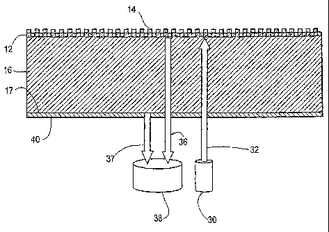
Referring to FIG. 4, a preferred embodiment of a biosensor is shown in cross
section. The sensor includes a grating layer 12 applied to a substrate 16,
which may
be a PET film. High index of refraction material 14 is deposited on the
grating layer
12. The lower surface 17 of the substrate has applied thereto an optically
diffuse layer
40. The layer 40 may take the form of a matte coating (UV cured acrylate-based
material), a roughening of the surface 17 or a grating applied to the surface
17. It is
possible to purchase from manufacturers PET film pre-coated with a cured UV
CA 02578625 2007-02-21
WO 2007/001597 PCT/US2006/014429
acrylate matte finish layer on one side (known in the art as an anti-glare
hard coating).
This embodiment is presently preferred, as it avoids the sensor manufacturer
of
having to take additional process steps to a base PET film to either roughen
it or add
the grating layer.
The construction of Figure 4 overcomes an optical interference problem that
would otherwise occur without the usage of the layer 40, e.g., in the
embodiment of
Figures 1-3. In particular, any two optically distinct interfaces within the
biosensor
construct will generate an optical interference spectral pattern. Light waves
reflecting
from two interfaces and traveling in the same direction interfere
constructively (when
in-phase) or destructively (when out of phase). Constructive interference
results in
higher intensity. Destructive interference results in lower intensity. In the
case of
normal incidence, destructive interference occurs when 2nd = in A/2, where d
represents the distance between interfering interfaces along the optical axis,
A a
particular wavelength, n the refractive index of the media between the
interfaces, and
in an integer. Constructive interference occurs when 2nd = in A. For fixed d
and n,
intensity will modulate, high and low, across a spectral range. Interference
effects
occur both with reflected light and transmitted light as well as with varying
angle of
incidence.
With continued reference to Figure 4, this invention addresses, primarily,
interference of light 37 reflected from the substrate/air interface (17) with
light 36
reflected by the biosensor active surface. These surfaces 12 and 17 produce
the
largest reflected intensity, which results in the most significant
interference effect. In
addition, the relatively large substrate 16 thickness, causes interference
maxima and
minima to have close spectral spacing; spacing on the order of useful spectral
features
produced by the biosensor. This similarity of spectral periodicity, between
the
11
CA 02578625 2007-02-21
WO 2007/001597 PCT/US2006/014429
substrate interference and the biosensor information signal, increases sensor
signal
uncertainty.
Observation of the reflected or transmitted spectrum from the substrate-
biosensor construct thus results in a periodic modulation of intensity as a
function of
wavelength superimposed upon the reflection or transmission characteristic of
the
active biosensor surface e.g. a sharp resonance peak. The period and position
of the
interference extrema depend upon subtle spatial variation of the substrate
thickness as
well as the wavelength of operation, and therefore the characteristics of the
modulation are not completely predictable nor spatially uniform.
Referring again to Figure 4, to address the problem, in a first aspect a
substrate
structure 16 is provided that eliminates the effects of optical interference
by
incorporating a roughened or "non-specular" surface 40 on the side of the
substrate
opposite the biosensor's illumination and detection apparatus 30 and 38. As
noted,
one can generate a useful roughened surface 40 in a number of ways in
accordance
with this disclosure, including (1) by adding a coating of optically diffuse
material to
the substrate bottom surface 17 (or purchasing the substrate 16 from a
supplier with
the coating already applied), (2) by etching the surface 17 to form a
roughened
surface 40, or (3) by applying a grating structure to the surface 17.
The diffuse coating can, for example, consist of a relatively hard cross-
linked
polymer material containing transparent particles sized to yield an
appropriate surface
roughness.
Etch treatment of the substrate surface 17 may be performed, for example, in a
plasma chamber. The resulting etching can produce a surface with finer
features.
A grating, embossed or printed on the surface 17, can produce a similar
effect.
Methods of applying a grating to a sensor substrate are disclosed in the
United States
12
CA 02578625 2007-02-21
WO 2007/001597 PCT/US2006/014429
Provisional patent application of Stephen Schulz filed on the same date as
this
application, "An Optimized Grating Based Biosensor and Substrate Combination,"
attorney docket no. 05-547. The additional back side grating acquires
antireflective
properties. This method of solving the interference problem, however,
presently
increases sensor cost prohibitively. However, this may be remedied as
technology
improves.
The patent literature, in the area of displays, touchscreens, or photographic
reproduction, contains examples of similar surface treatments for elimination
of
"Newton rings". See e.g., U.S. Patents 6,592,950 and 6,555,235. Newton rings
refer
to visible and spatially distributed interference patterns generated, for
example, by a
small air gap. "Anti Newton ring" (ANR) treatments or coatings destroy the
coherence of light reflected from one or both surfaces comprising the air gap.
In the
case of a biosensor, the troublesome interference pattern arises from
interference
within the substrate rather than between two substrates. The interference
fringes that
occur within the biosensor substrate have much closer spectral spacing making
them
invisible to the eye but disruptive to sensor operation. The application of
such ANR
techniques to the field of optical biosensors is believed to be novel.
The layer 40 applied to the surface 17 of the substrate structure 16, as
described herein, eliminates optical interference between the upper and lower
surfaces
of the substrate by preventing light reflected from this lower surface from
aligning
coherently with light reflected from an upper interface between the substrate
16 and
the grating 12. The invention is particularly useful for optical biosensors
where
measurement sensitivity depends on detecting small changes in the spectral
distribution of the reflected or transmitted spectra. In this case, spectral
modulation
13
CA 02578625 2007-02-21
WO 2007/001597 PCT/US2006/014429
caused by interference, superimposed onto the biosensor optical signal, adds
error and
decreases sensor resolution.
The problem of interference in optical biosensors has been addressed in
several different ways in the prior art, all with their own attendant
disadvantages.
1. Boxcar averaging
The optical interference effect can be mathematically removed from a biosensor
reflectance or transmittance spectra by a technique called boxcar averaging. A
reflectance or transmittance spectra is typically gathered over a wide range
of
wavelengths by a series of discreet measurements taken at small intervals. For
any
particular wavelength, A, the next closest measurements in the spectra will be
A +D A,
and A -D A, where D A represents the wavelength interval, in practice
determined by
the spectrometer hardware. Boxcar averaging determines, for all A, an averaged
response and the neighboring responses over a specified interval, b, called
the "boxcar
length." The new, averaged spectra, g(A), can be calculated from the measured
spectra, f(A), by the formula:
+b
90 2b + 1 ~ (f (A + nAA))
The boxcar average will provide a smoothed reflectance spectra by averaging
the high and low portions of the spectra generated by the interference effect.
This
approach has some disadvantages. Primarily, the interference period cannot
always be
predicted given process variations during the manufacture of the biosensor.
The actual
use of the biosensor also changes the interference period. To achieve optimum
results,
one would need to analyze the spectrum for interference and then tune the
boxcar
average to the specific circumstance. Secondly, the averaged spectrum
represents a
"lower resolution" version of biosensor's optical response. The averaging
process
14
CA 02578625 2007-02-21
WO 2007/001597 PCT/US2006/014429
may obscure subtle shifts of the spectrum produced by binding of biochemical
material. To effectively remove the spectral modulation induced by
interference, one
must average over a range that approximates the period of the interference,
ideally
more that one period. If the interference modulation has a period similar to
important
biosensor spectral features (e.g. resonance peak) then averaging can
effectively flatten
the biosensor's spectral response and limit detection of small response
changes.
2. Antireflective coating
Given that interference effects occur between light waves reflected from two
surfaces, suppressing reflection from either surface diminishes interference.
Hence,
application of an antireflective (AR) coating to the substrate surface 17
opposite the
biosensor optical components cail diminish the superposition of interference
modulation on the biosensor response. AR coatings reduce the reflected
intensity
from a boundary between two materials of differing refractive index over a
predetermined "design" wavelength range. Typically, AR coatings consist of
thin
films of dielectric materials applied with high accuracy by processes such as
evaporation or sputtering. The thickness, refractive index, and number of
layers
comprising a thin-film based AR coating determine its useful spectral width,
location,
and reflection level. Minimizing the reflected energy from the substrate-air
interface
on the surface opposite the active biosensor minimizes interference from light
reflected by that surface.
Application of AR coatings adds considerable cost compared with the solution
offered by this invention. Furthermore, staining or scratching the bottom
surface of
an AR coated biosensor produce renders the AR coating ineffective. The diffuse
coatings employed by this invention have exceptional durability and can be
obtained
at low cost.
CA 02578625 2007-02-21
WO 2007/001597 PCT/US2006/014429
3. Use of Nonplanaf= substrate
Optical interference between the front and back surfaces of a biosensor
substrate can be reduced or eliminated if the front and back surface of the
substrate
are not parallel to each other. In this case, light reflected from the top and
bottom
surfaces of the substrate are not parallel to each other and do not have the
opportunity
to constructively and destructively interfere. This solution does not lend
itself well to
high volume manufacturing on bulk planar substrate material.
Functional advantages
Using the teachings of this disclosure, a number of advantages are obtained:
1. Accuracy and simplicity in measuring small shifts in biosensor reflectance
or
transmittance characteristics is obtained as compared to boxcar averaging
techniques.
2. The biosensor is well-suited for use in systems where the biosensor peak
wavelength value is obtained by a laser - due to the higher likelihood for
coherence.
3. Lower cost (-lOx) compared to the cost of deposition of antireflective
coatings on the sensor surface.
4. The solution allows for an implementation of a biosensor detection
instrument
that measures the biosensor by illuminating the sensor at normal, or near
normal, angles of incidence. Normal or near normal is most convenient for
simple and robust optical alignment of illumination source and detector.
16
CA 02578625 2007-02-21
WO 2007/001597 PCT/US2006/014429
Example
Figure 5 shows two graphs of intensity as function of wavelength, with one
graph represented by line 40 for a sensor of the type shown in Figures 1-3 and
the
other (line 42) for a sensor of the type shown in Figure 4 with the layer 40
formed as
a matte cross-linked polymer acting as an optically diffuse layer. Note in
Figure 5 the
interference between the reflected light from the biosensor active surface and
the
lower surface of the substrate creates a local maximum 46, and this maximum
due to
interference can create an error in the calculation of the location of the
resonance
peak. Note also the interference fringes 44 in the line 40. However, with the
biosensor construction of Figure 4, the line 42 does not have any interference
fringes
or local maxima (as in the case of 46) to skew or cause error in the
calculation of the
peak resonance frequency. Similar results would be expected for surface
roughening
of the layer 17 or by applying a grating to the lower surface 17 of the sensor
substrate.
While a number of exemplary aspects and embodiments have been discussed
above, those of skill in the art will recognize certain modifications,
permutations,
additions and sub-combinations thereof. It is therefore intended that the
appended
claims and claims hereafter introduced are interpreted to include all such
modifications, permutations, additions and sub-combinations as are within
their true
spirit and scope.
17