Note: Descriptions are shown in the official language in which they were submitted.
CA 02579426 2007-03-06
WO 2006/043980 PCT/US2005/014859
1
-ELECTRONIC CONTROL ENCLOSURE
FIELD OF THE INVENTION
[0001] This invention pertains generally to electronic control units and more
particularly to
an electronic control enclosure for housing the electronic components of an
electronic control
unit and that is configured to dissipate heat from within the enclosure.
BACKGROUND OF THE IlWENTION
[0002] Electronic control units are typically used in various applications to
control
electronic or electrical devices and, accordingly, are made of many electronic
components.
Often, the electronic components are mounted to a printed circuit board to
both establish
electrical communication between the components and to keep the components in
a tightly
grouped assembly. To protect the electronic components from damage due to
impact with
external objects and to simplify distribution and attachment of the electronic
control unit, the
components are also often housed in a protective enclosure housing.
[0003] In some applications, the electronic control unit is required to be
placed in a
particularly harsh environment. For instance, the electronic control unit may
be placed in or on
an automobile or similar transportation mechanism to control, for example, the
timing and
operation of the engine. Such applications may expose the electronic control
unit to airbome
dirt and grime that, if allowed to enter the enclosure housing, could damage
the electronic
components. Therefore, it is often desirable that the enclosure housing be
environmentally
sealed. However, because the electronic components located in the enclosure
housing typically
generate heat energy during operation that could potentially damage the
components, measures
must be taken to cool the components.
BRIEF SUMMARY OF THE INVENTION
[0004] The invention provides an electronic control enclosure for protectively
housing and
removing heat energy from the components of an electronic control unit. The
electronic
control enclosure includes an enclosure housing that defines an interior
chamber in which the
electrical components can be protectively placed. To establish electrical
communication
between the electrical components and one or more extemal electrical sources,
the electronic
control enclosure also includes a header assembly and a substrate assembly.
The header
assembly includes a front plate into which receptacles are formed that can
receive electrical
cables and plugs from the external sources. Attached to the header assembly is
a substrate of
the substrate assembly that has conductive traces formed thereon. Mounted to
the substrate in
CA 02579426 2007-03-06
WO 2006/043980 PCT/US2005/014859
2
an integrated fashion are various elements that make up the electronic control
unit. Among
these elements are electronic components that, because they generate heat
energy during their
operation, include exposed heat transfer surfaces for dissipating the heat
energy. An example
of such electronic components are discrete transistors such as MOSFET devices.
[0005] To remove the generated heat from the electronic components, in one
aspect of the
invention, the electronic control unit includes a heat sink having both an
interior surface
exposed to the interior chamber and an exterior surface exposed at the
exterior of the enclosure
housing. The heat sink can be disposed through the enclosure housing. In other
embodiments,
the enclosure housing may be made of a heat conductive material, such as
metal, and the heat
sink is integral with the enclosure housing. When the header assembly is
inserted into the
interior chamber, the electronic components mounted to the substrate align
along the heat sink.
To ensure that heat energy is adequately transferred from the electronic
components to the heat
sink and thereby removed from the interior chamber to the exterior surface, a
spring is located
within the interior chamber that urges the heat transfer surfaces toward the
interior surfaces: -
[0006] In another aspect of the invention, the heat sink can be formed as part
of the header
assembly. The electronic components are mounted to or otherwise in direct
contact with the
heat sink. The substrate, with its electrical traces, is also attached to the
header assembly and
electrical communication is established between the electronic components and
the substrate.
Once the header assembly is inserted into the interior chamber, heat generated
from the
electronic components is transferred via the heat sinks to the exposed
portions of the header
assembly where the heat energy is dissipated to the exterior environment.
[0007] An advantage of the invention is that it provides an electronic control
enclosure for
protectively enclosirig the electronic components of an electronic control
unit. Another
advantage is that the invention removes heat eneirgy generated by the
electronic components
and transfers that heat energy to the exterior of the electronic control
enclosure. Another
advantage is that the invention is configured to improve the transfer of heat
energy between an
exposed heat transfer surface of the electronic components and a heat sink.
These and other
advantages and features of the invention will become apparent from
the'foregoing detailed
description and drawings.
BRIEF DESCRIPTION OF THE DRAWINGS
[0008] Figure 1 is a top perspective view of an electronic control enclosure
for protectively
housing the electronic components of an electronic control unit, including two
plugged-in
cables.
CA 02579426 2007-03-06
WO 2006/043980 PCT/US2005/014859
3
[0009] Figure 2 is a bottom perspective view of the electronic control
enclosure of Figure
1, illustrating the exterior surfaces of two heat sinks for transferring heat
from an interior
chamber.
[0010] Figure 3 is a top plan view of the electronic control enclosure of
claim 1.
[0011] Figure 4 is an exploded view of the electronic control enclosure of
claim 1,
illustrating the parts of the control enclosure including the electronic
components.
[00121 Figure 5 is a cross-sectional view taken along line 5-5 of Figure 3
illustrating a
header assembly environmentally sealing an enclosure housing.
[0013] Figure 6 is a perspective view of the electronic control enclosure of
Figure 1,
illustrating the header assembly and an attached substrate assembly being
inserted into the
enclosure housing.
[0014] Figure 7 is a perspective view of a spring plate for urging the
electronic components
against heat sinks in the electronic control enclosure of Figure 1.
[0015] Figure 8 is a cross-sectional view of the electronic control enclosure
taken along
line 8-8 of Figure 3.
[0016] Figure 9 is a top perspective view of the electronic control enclosure
with.the top
wall removed and the header assembly and substrate assembly substantially
inserted to a pre-
load position.
[0017] Figure 10 is a top perspective view of the electronic control enclosure
with the top
wall removed and the header assembly and substrate assembly fully inserted to
a loaded
position.
[0018] Figure 11 is a top plan view of another embodiment of an electronic
control
enclosure for protectively housing the electronic components of an electronic
control unit.
[0019] Figure 12 is a top perspective view of the electronic control enclosure
of Figure 11,
illustrating a header assembly and a substrate assembly being inserted into an
enclosure
housing.
[0020] Figure 13 is a cross-sectional view taken along li.ne 13-13 of Figure
11 illustrating
the header assembly and substrate assembly inserted into the enclosure
housing.
[0021] Figure 14 is a cross-sectional view taken along line 14-14 of Figure 11
with the
header assembly and substrate assembly inserted into the enclosure housing.
[0022] Figure 15 is a first side perspective view of the electronic control
enclosure with the
side removed to illustrate the header assembly and substrate assembly as
substantially inserted
to a pre-load position.
CA 02579426 2007-03-06
WO 2006/043980 PCT/US2005/014859
4
[0023] Figure 16 is a first side perspective view of the electronic control
enclosure with the
side removed to illustrate the header assembly and substrate assembly as fully
inserted to a
loaded position.
[0024] Figure 17 is a perspective view of a spring plate for urging electronic
components
toward heat sinks in the electronic control enclosure of Figure 11.
[0025] Figure 18 is a front perspective view of another embodiment of an
electronic control
enclosure for protectively housing the electronic components of an electronic
control unit.
[0026] Figure 19 is a top plan view of the electronic control enclosure of
Figure 18.
[0027] Figure 20 is a top perspective view of an enclosure housing defining an
interior
chamber for receiving the electronic components of the electronic control
enclosure of Figure
18.
[0028] Figure 21 is a bottom perspective view of the enclosure housing
iIlustrated in Figure
20.
[0029] Figure 22 is a cross-sectional view taken along line 22-22 of Figure 19
illustrating a
header assembly and a substrate assembly inserted into the enclosure housing.
=
[0030) Figure 23 is a detailed view of the indicated area of Figure 22
illustrating the
substrate assembly as substantially inserted in the enclosure housing to a pre-
load position.
[0031] Figure 24 is a detailed view of the indicated area of Figure 22
illustrating the
substrate assembly as fully inserted in the enclosure housing to a loaded
position.
[0032] Figure 25 is a top perspective view of another embodiment of an
electronic control
enclosure for protectively housing the electronic components of an electronic
control unit.
[0033] Figure 26 is a rear perspective view of a header assembly and a
substrate assembly
for the electronic control enclosure of Figure 25.
[0034] Figure 27 is a side elevational view of the header assembly and
substrate assembly
of Figure 26.
[0035] Figure 28 is an exploded view of the header assembly and substrate
assembly of
Figure 26.
[0036] Figure 29 is a perspective view of another embodiment.
[00371 Figure 30 is a cross-sectional view of the embodiment shown in Fig. 29.
DETAILED DESCRIPTION OF THE INVENTION
[0038] Now referring to the drawings, wherein like reference numbers refer to
like
elements, there is illustrated in FIGS. 1, 2 and 3 the exterior of an
embodiment of an electronic
control enclosure 100 for an electronic control unit designed in accordance
with the teachings
of the invention. The electronic control unit can be used to control
externally situated electrical
CA 02579426 2007-03-06
WO 2006/043980 PCT/US2005/014859
devices. The electrical elements and components making up the electronic
control unit are
located in the interior of the electronic control enclosure 100, where they
are protected from the
exterior environment. To establish communication between the internal elements
and
components and the externally situated electrical devices, one or more
electrical cables 102 that
terminate in plugs 103 are plugged into the electronic control enclosure 100.
[0039] The electronic control enclosure 100 can be secured to a panel 104
situated
proximate to the external electrical devices with one or more fasteners 106,
though, in other
embodiments, the electronic control enclosure can be secured by other
appropriate securing
methods. Referring to FIGS. 1, 2, and 3, the electronic control enclosure 100
preferably has a
generally overall rectangular shape with a low profile so that the electronic
control unit will not
interfere with other devices situated the surrounding environment. Because the
elements and
components making up the electronic control unit are protectively housed in
the electronic
control enclosure 100, the electronic control unit can be secured within harsh
or dirty
environments, such as the engine compartment of an automobile. '
[0040] Illustrated in FIG. 4 are the various parts that make up the electronic
control
enclosure 100. To define an interior chamber 112 for the electronic
components, an enclosure
housing 110 is provided. The enclosure housing 110 has a top wall 114, an
opposing bottom
wall 116, and first and second sidewalls 118, 119 that extend between the top
and bottom walls
114, 116. The top, bottom, and sidewalls are integrally joined and arranged
generally
orthogonally with each other to produce the rectangular shape of the
electronic control
enclosure. To enclose the interior chamber 112, a rear wall 120 extends
adjacent to and is
likewise integrally joined with the top, bottom, and sidewalls. As will be
appreciated, the terms
"top," "bottom," "side," and "rear" are exemplary only and are not intended to
limit the
orientation of the enclosure housing or the electronic control enclosuie in
any way.
[0041] The enclosure housing can be made from any suitable niaterial such as,
for instance,
molded plastic that preferably demonstrates corrosion resistant properties. To
shield the
components of the electronic control unit that are housed in the interior
chamber from
electrical-magnetic interference, the inner surfaces of the top, bottom, side,
and rear walls can
be coated with an EM! shielding material. In other embodiments, the enclosure
housing can be
made from a metallic material.
[0042] To access the interior chamber, the portion of the enclosure housing
110 opposite
the rear wal1120 is formed as an opening 126. The opening 126 is defined by a
rectangular rim
128 that is formed by the forward-most edges of the top, bottom, and sidewalls
114, 116, 118,
119. Extending from either sidewall 118, 119 and projecting forward of the rim
128 are
cantilevered latch arms 130 that terminate in inclined barbs 132. To secure
the electronic
CA 02579426 2007-03-06
WO 2006/043980 PCT/US2005/014859
6
enclosure housing to the panel, there is projecting from either sidewall 118,
119 proximate to
the bottom wal1116 one or more mounting feet 134 through which the fasteners
106 can be
inserted.
[0043] To enclose the opening 126 while establishing electronic communication
with the
interior chamber 112, the electric control enclosure also includes a header
assembly 140. The
header assembly 140 has a generally planar front plate 142 that is sized to be
received in the
opening 126 and constrained within the rim 128. One or more electrical
terminals 144 extend
through the front plate 142 and are retained by the front plate in a
predetermined arrangement.
To protect the external portions of the terminals 144 from damage and to
appropriately align
the plugs 103 with the arranged terminals, there extend from the front plate
142 one or more
receptacle walls 146 that surround the terminals.
[0044] The front plate 142 and receptacle walls 146 can be manufactured from
any suitable
material, such as plastic, cast aluminum or magnesium. To fasten the header
assembly 140 to
the enclosure housing 110, there are extending from either side of the front
plate 142 latch -
catches 148. When the front plate 142 is aligned with the rim 128 that defines
the opening 126,
the latch catches 148 likewise align with the latch arms 130. Referring to
FIGS. 2 and 4, as the
header assembly 140 and enclosure housing 110 are moved together, the
cantilevered latch
arms 130 are received in and extend through slots 150 defined by the latch
catches 148. The
latch catches 148 and the inclined barbs 132 at the end of the latch arms 130
are configured to
initially deflect the cantilevered latch arms outward from the sidewalls 118,
119. However,
once the front plate 142 is constrained within the rim 128, it will be
appreciated that the
inclined barbs 132 extend around and hook onto the latch catches 148, thereby
retaining the
header assembly and enclosure housing together. It will be appreciated that by
using the
appropriate tools, the inclined barbs 132 can be unhooked from the latch
catches 148 to remove
the header assembly from the enclosure housing. It will further be
appreciate'd that in other
embodiments, the latch arms can be included on the front plate and the latch
catches can be
included on the enclosure housing.
[0045] To environmentally seal the interior chamber 112 when the header
assembly and
enclosure housing are retained together, referring to FIG. 5, a peripheral
seal 152 is included
between the front plate 142 and rim 128. The peripheral sea1152 can be made
from any
suitable material; such as a natural or elastomeric rubber. To facilitate the
setting and
engagement of the peripheral seal 152, the rim 128 is formed with a seating
surface 154 that
may invertedly slope rearward into the interior chamber 112. The seal 152 may
have a C-
shaped cross-section which includes a center portion 153, an inner leg 155 and
an outer leg
157. The seal 152 may include protrusions 158 and/or recesses 159 which assist
in creating a
CA 02579426 2007-03-06
WO 2006/043980 PCT/US2005/014859
7
seal between the housing and the front plate. The peripheral seal may be
placed against the rim
of the enclosure housing before the front plate and the enclosure housing are
retained together.
The seal 152 fits over the seating surface 154 and the inner rim of the
housing. The front plate
142 includes a complementary boss 156 projecting from the side of the front
plate opposite the
receptacle walls 146. The boss 156 may slope rearward into the interior
chamber 112. As will
be appreciated, when the front plate 142 is set within the rim 128, the
peripheral seal 152 is
compressed between the boss 156 and the seating surface 154. Because the
interior chamber is
environmentally sealed, dirt and grime from the exterior environment cannot
enter the
enclosure housing.
[0046] Referring to FIG. 4, to mount and interconnect the various electronic
components of
the electronic control unit, the electronic control enclosure includes a
substrate assembly 160.
The substrate assembly 160 is arranged around a substrate 162, such as a
printed circuit board,
on which electrically conductive circuit traces are formed. The substrate 162
has a generally
planar shape with opposing first and second surfaces 168, 169. The substrate
162 can be --
rigidly attached to the header assembly 140 so as to extend rearwardly from
the lower edge of
the front plate 142.
[0047] As illustrated in FIGS. 4 and 5, to establish electrical communication
between the
cables from the external devices and the substrate assembly 162, the terminals
144 include
terminal leads 161 on the rear side of the front plate 142 that are formed
with right angles
directing the terminals toward the substrate. The terminal leads 161 are
soldered to and make
electrical contact with the conductive circuit traces on the substrate 162. To
prevent cross-talk
or inductive interference between the terminals 144, in an embodiment, the
header assembly
140 can also include an inductive ferrite filter block through which the
terminal leads 161 pass.
As will be appreciated by those of skill in the art, the filter block
physically separates the
terminals leads while it simultaneously shields the terminals from electro-
magnetic and
inductive interference.
[0048] The electronic components that make up the electronic control unit are
mounted to
the substrate 162 so that the electronic components are in electrical
communication with the
conductive circuit traces. A typical electronic component included in the
electronic control unit
is a discrete transistor that, as is familiar to those of skill in the
electronics arts, functions as an
electrical switch. One type of transistor particularly well-suited for the
electronic control unit
is a metal-oxide semiconductor field effect transistor (MOSFET). The MOSFET
includes one
or more leads, such as a gate, source, or drain lead, that are soldered to
lead holes disposed into
the substrate 162. Referring to FIG. 4, because such MOSFET devices 164
generate heat
energy during their operation that, if not removed, could adversely effect and
possibly damage
CA 02579426 2007-03-06
WO 2006/043980 PCT/US2005/014859
8
the MOSFET device, the MOSFET device may be provided with an exposed
heat'transfer
surface 166 made of a thermally conductive material.
[0049] Referring to FIG. 6, in the illustrated embodiment, the MOSFET devices
164
project upright from the first surface 168 and are arranged in two rows 170,
171 extending from
approximately near the front plate 142 rearward. The rows 170, 171 are aligned
along a first
and second side-edge 172, 174 of the substrate 162 such that the heat transfer
surfaces 166 are
directed outward. Within the rows 170, 171, the MOSFET devices 164 are
generally spaced-
apart from each other.
[0050] Also included as part of the substrate assembly 160, as illustrated in
FIGS. 4 and 6,
are one or more spring plates 178 that are mounted to the substrate 162.
Referring to FIG. 7,
the spring plate 178 is a generally planar, elongated structure that can be
made from any
suitable material, such as stamped sheet metal. To keep the MOSFET devices
spaced-apart, the
spring plate 178 includes multiple spacer elements 180 that extend along the
length of the
spring plate. The width of the spacer elements 180 is approximately equal to
the distance the
MOSFET devices are spaced-apart, while the distance between the spacer
elements is
approximately equal to the width of a MOSFET device. Located between the
spacer elements
180 and designed to individually contact the MOSFET devices are a plurality of
engagement
elements 182 that are also formed into the spring plate 178.
[0051] As illustrated in FIG. 6, when mounted to the substrate 162, the spring
plates 178
extend along the rows 170, 171 of MOSFET devices 164 with the spacer elements
and holder
elements appropriately engaging the MOSFET devices. Referring to FIG. 7, to
mount the
spring plate 178 to the substrate 162, one or more attachment prongs 184
extend from the
spring plate 178 that can be received within complementary slots disposed into
the substrate.
One of the attachment prongs 184 can also include a locking prong 186 for
locking the spring
plate 178 in an upright position on the substrate 162. '
[0052] As illustrated in FIG. 6, to place the MOSFET devices 164 in the
interior chamber
112 so that they are protectively enclosed within the enclosure housing 110,
the substrate
assembly 160 is inserted through the opening 112 toward the rear wall 120
until the front plate
142 engages against the rim 128. The housing 110 may include raised surfaces
or rails 187,
189 to support the substrate 162 as shown in Figs. 5, 6 and 8. Referring to
FIG. 8, once
inserted into the interior chamber 112, the substrate 162 extends orthogonally
between the first
and second sidewalls 118, 119 with the first surface 168 opposing and spaced-
apart from the
top wall 114 and the second surface 169 opposing the bottom wall 116. Because
of the sealing
engagement between the header assembly and the opening, the electronic
components 164 are
all environmentally sealed within the interior chamber 112.
CA 02579426 2007-03-06
WO 2006/043980 PCT/US2005/014859
9
100531 Attaching the peripheral seal to the rim prior to engaging the front
plate-with the
enclosure housing, as described above, facilities assembly of the substrate
assembly by
enabling reflow or wave soldering. Specifically, as will be appreciated by
those of skill in the
art, the terminal leads from the header assembly and the electronic components
are mounted to
the circuit traces on the substrate. The header assembly and substrate
assembly may then be
subjected to the reflow or wave soldering operation that permanently mounts
the terminal leads
and electrical 'components to the substrate in such a manner as to establish
electrical
communication between the various parts. Because the peripheral seal is safely
mounted on the
enclosure housing which does not undergo the soldering process, the peripheral
seal will
remain undamaged.
[0054] To remove heat energy from the electronic components and thereby
prevent
overheating of the sealed interior chamber, in accordance with an aspect of
the invention, the
enclosure housing includes one or more heat sinks. In the embodiments where
the enclosure
housing is plastic, the heat sinks may be disposed through the enclosure
housing. In the --
embodiments with the plastic housings, the heat sinks are made from an
appropriate, thermally-
conductive material such as aluminum, magnesium, zinc, or alloys thereof, or a
heat conduative
plastic and are arranged in the enclosure housing so as to conduct heat energy
from the interior
chamber to the exterior environment. In the embodiments where the enclosure
housing is heat
conductive material, such as metal, the heat sinks may be integral with the
enclosure housing.
The heat conductive material may be aluminum, magnesium, zinc, or alloys
thereof, or a heat
conductive plastic.
[0055] Referring to FIG. 8, there is illustrated a first and a second heat
sink 190, 192 that
are disposed through the bottom wall 116 and therefore are partially located
within the interior
chamber 112. Accordingly, the heat sinks 190, 192 each include an interior
surface 196 that is
exposed within the interior chamber 112 and an exterior surface 198 that is
exposed along the
exterior of the bottom wall 116, as illustrated in FIGS. 2 and 8. Referring to
FIGS. 8, 9, and
10, the elongated first and second heat sinks 190, 192 extend along the height
of first and
second sidewalls 118, 119 such that the interior surfaces 196 oppose each
other across the
substrate 162. To accommodate and retain the heat sinks 190, 192, slots can be
formed through
the bottom wall 120 to which the heat sinks are adhered with epoxy.
[0056] Referring to FIGS. 6 and 8, due to the arrangement of the MOSFET
devices 164
along the first and second edges 172, 174 of the substrate 162, when the
substrate assembly is
inserted into the interior chamber 112, the rows 170, 171 of MOSFET devices
align with the
elongated heat sinks 190, 192. Moreover, the exposed heat transfer surfaces
166 of the
MOSFET devices oppose and are adjacent to the interior surfaces 196 of the
heat sinks 190,
CA 02579426 2007-03-06
WO 2006/043980 PCT/US2005/014859
192. Heat energy generated by the MOSFET devices 164 is thereby conducted from
the heat
transfer surfaces 166 through the heat sinks 190, 192 to the exterior surfaces
198.
[0057] To ensure that the thermal energy is adequately transferred from the
electronic
components 164 to the heat sinks 190, 192, in accordance with another aspect
of the invention,
the spring plates 178 can urge the MOSFET devices 164 toward the interior
surfaces 196. To
make the spring plates 178 urge the MOSFET devices 164, referring to FIGS. 8,
9, and 10, the
enclosure housing 110 includes an embossment 200 projecting into the interior
chamber 112.
In the illustrated embodiment, the embossment 200 projects from the top wall
114 towards the
bottom wall 116 and can be formed when the enclosure housing is molded. The
embossment
200 includes a first edge 202 that is oriented toward and spaced-apart from
the first sidewall
118 and further includes a second edge 204 that is oriented toward and spaced-
apart from the
second sidewal1119. Furthermore, the first and second edges 202, 204 extend
generally
parallel to the first and second sidewalls 118, 119.
[0058] When the substrate assembly is inserted into the interior chamber, as
illustrated irr
FIG. 8, the MOSFET devices 164 are located in the spaces between the first
an,d second edges
202, 204 and the first and second sidewalls 118, 119. The embossment 200
contacts the spring
plates 178 urging the spring plates toward the respective first and second
sidewalls 118, 119.
Because of the arrangement of the MOSFET devices 164 on the substrate 162, the
heat transfer
surfaces 166 are urged against the interior surfaces 196 of the heat sinks
190, 192 thereby
ensuring that the generated heat energy is adequately transferred.
[0059] To insert the substrate assembly into the interior chamber 112 without
damaging the
MOSFET devices 164, the embossment 200 and spring plates 178 are configured to
only
engage each other after the substrate assembly is fully inserted to a loaded
position. To
accomplish this, as illustrated in FIGS. 9 and 10, the first and second edges
202, 204 both
include a step 206 that divides the first and second edges into first and
second edge portions
208, 210. The first edge portion 208 is spaced a greater distance from the
first and second
sidewalls 118, 119 than the second edge portion 210 is spaced. Moreover, the
first edge
portion 208 is spaced from the rear wall 120 while the second edge portion 210
is proximate to
the rear wall. Additionally, referring to FIG. 7, the spring plate 178 also
includes first and
second compression features 212, 214 that protrude from the spring plate 178.
Moreover, the
first compression feature 212 protrudes further from the plane of the spring
plate 178 than the
second compression feature 214, with the first compression feature oriented
further forward on
the spring plate than the second compression feature. The first and second
compression
features can be formed by displacing a portion of the spring plate through a
stamping operation.
CA 02579426 2007-03-06
WO 2006/043980 PCT/US2005/014859
11
[0060] Referring to FIG. 9; it will be appreciated thafi'as the substrate
assembly is inserted,
the smaller second compression feature 214 is loosely received in the gap
between the first
edge portion 208 and the respective sidewall. This position is known as the
pre-load position,
which exists over a substantial range of insertion of the substrate assembly,
wherein the
embossment and spring plate do not significantly urge the MOSFET devices
toward the heat
sinks. Accordingly, as will be familiar to those of skill in the art, the
electronic control
enclosure demonstrates a zero insertion force effect in which no substantial
resistance is
encountered during insertion of the substrate assembly to the preload
position. However,
referring to FIG. 10, as the second compression feature 214 passes over the
step 206 and
engages the second edge portion 210, the spring plate 178 is directed toward
the respective
sidewall and against the MOSFET devices 164. Additionally, onee the substrate
assembly is
fully inserted, the larger first compression feature 212 engages the first
edge portion 208
likewise causing the spring plate 178 to urge the MOSFET devices 164 against
the heat sinks
190, 192. This is known as the loaded position, wherein once the substrate
assembly is fully-
inserted, the embossment and spring plate significantly urge the MOSFET
devices towards the
heat sinks.
[0061] Because the MOSFET devices 194 contact the heat sinks 164 after the
compression
features and edge portions have engaged, destructive sliding of the heat
transfer surfaces 166
over the interior surfaces 196 is reduced. The edge portions and compression
features can be
configured to engage only over the last 0.1 inches of insertion. In an
embodiment, to assist in
transferring heat energy away from the MOSFET devices, a thermal conducting
paste,
adhesive, or pad can be placed between the heat transfer surfaces and the
interior surfaces.
Thermal conducting paste or pads may further reduce the destructive sliding.
[0062] In another embodiment, the heat sinks may be removed from the enclosure
housing
if the heat sinks are not needed. The openings in the housing where the heat
sinks would
extend through the housing would be covered with housing material. For
example, Figs. 29
and 30 show one embodiment with the heat sinks removed from the embodiment
shown in
Figs. 8 and 9. If desired, the heat sinks may be removed from the other
embodiments as
appropriate.
[0063] In addition, the enclosure housing may include a channel to engage the
substrate.
Referring to Figs. 29 and 30, the housing 610 may include channels 680, 682
which will
engage the substrate 662. The channels 680, 682 may assist in preventing the
substrate 662
from moving vertically if the housing is subjected to movement.
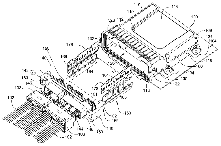
[0064] Illustrated in FIGS. 11 through 16 is another embodiment of the
electronic 'control
enclosure 300 for housing the components of an electronic control unit. As
illustrated in FIG.
CA 02579426 2007-03-06
WO 2006/043980 PCT/US2005/014859
12
11, the electronic control enclosure 300 is generally rectangular with a low
profile so that the
electronic control enclosure will not interfere with other devices situated in
the same
environment. Referring to FIG. 12, the electronic control enclosure 300
includes an enclosure
housing 302 that defines an interior chamber 304 into which the electronic
components can be
inserted. The enclosure housing 302 includes a top wall 310, an opposing
bottom wall 312, and
first and second sidewalls 314, 316 extending between the top and bottom
walls. A rear wall
318 extends across and is joined to the rear edges of the top, bottom, and
sidewalls to enclose
the enclosure housing 302. The enclosure housing can be made from injection
molded plastic.
In other embodiments, the enclosure housing may be made from a heat conductive
material,
such as metal.
[0065] To access the interior chamber 304, the forward portion of the
enclosure housing=
302 opposite the rear wall 318 is formed as an opening 320. The opening 320 is
defined by a
rim 322 made up of the forward-most edges of the top, bottom, and sidewalls
310, 312, 314,
316. To establish electronic communication with the electronic components
inside the --
enclosure housing 302 while simultaneously enclosing the interior chamber 304,
there is
included as part of the electronic control enclosure 300 a header assembly
330. The header assembly 330 includes a front plate 332 that can be received
within the opening 320 so as to
environmentally seal the interior chamber 304. Extending forward from the
front plate 332 are
one or more receptacle walls 334 in which plugs can be received. To attach the
header
assembly 330 to the enclosure housing 302, latch arms 324 and latch catches
336 are provided
that function as described above.
[0066] To mount and interconnect the various electronic components of the
electronic
control unit, the electronic control enclosure 300 includes a substrate
assembly 340. The
substrate assembly 340 includes a generally planar substrate 342 having a
first surface 344 and
an opposing second surface 345 to which electronic components, such as MOSFET
devices
350, can be mounted. In the illustra.ted embodiment, the MOSFET devices 350
are arranged
into two rows 352, 354, each extending from the front plate 332 rearward along
the first and
second side-edges 346, 347 of the substrate 342. The MOSFET devices 350 are
laid
horizontally flat with their heat transfer surfaces 356 adjacent to the
substrate 342.
Furthermore, the substrate 342 is rigidly attached to and extends rearward
from the front plate
332 of the header assembly 330.
=[0067] To remove heat generated from the MOSFET devices 350, referring to
FIG. 12, the
electronic control enclosure 300 includes a first heat sink 360 and a second
heat sink 362. The
first and second heat sinks 360, 362 may be disposed through the bottom wall
312 so as to
generally extend along the respective first and second sidewalls 314, 316. In
the embodiment
CA 02579426 2007-03-06
WO 2006/043980 PCT/US2005/014859
13
illustrated in FIGS. 13, 14, 15, and 16, the first and secondheat sinks 360,
362 each have an
interior surface 364 and an exterior surface 366. The interior surface 364 is
generally parallel
to and slightly offset above the bottom wall 312 while the exterior surface
366 is parallel to and
offset below the bottom wall. Referring to FIG. 14, when the substrate
assembly is inserted
into the interior chamber 304, the substrate 342 extends between the first and
second sidewalls
314, 316 and overlies the interior surface 364 of the heat sinks 360, 362. In
other
embodiments, the enclosure housing may be made of a heat conductive material,
such as metal,
and the heat sink is integral with the enclosure housing.
[0068] Referring to FIG. 14, to transfer the heat energy generated by the
MOSFET devices
350 to the heat sinks 360, 362, the substrate 342 includes multiple apertures
370 disposed
between the first and second surfaces 344, 345 that align with the heat
transfer surfaces 356 of
the MOSFET devices. Located in each aperture 370, so as to contact both the
heat transfer
surfaces 356 and the interior surface 364, is a heat conductive element 372,
such as a solder, or
other low melting heat transferable materials. Accordingly, the heat
conductive elements 372
transfer the heat across the substrate 342. ,
[0069] To ensure adequate thermal contact between the MOSFET devices 350 and
the heat
conducting elements 372, as illustrated in FIGS. 14, 15, and 16, the
electronic control enclosure
includes spring plates 380 and embossments 390, 392 that are capable of
engaging each other.
Referring to FIG. 17, the spring plate 380 includes an elongated compression
leg 382 that
terminates at one end in an attachment foot 384. The attachment foot 384
curves
approximately ninety degrees with respect to the orientation of the
compression leg 382.
Protruding from the compression leg 382 are first and second compression
features 386, 388,
the first compression feature protruding a greater distance from the plane of
the compression
leg than the second compression feature. Additionally, the first compression
feature 386 is
located further away from the attachment foot 384 than the second compression
feature 388.
The spring plate 380 can be made from any suitable material, such as, for
example, sheet metal
that has been stamped and formed.
[0070] Referring to FIGS. 15 and 16, the spring plates 380 are mounted to the
substrate 342
so that the compression leg 382 extends over the MOSFET devices 350 and the
attachment leg
384 is attached to the substrate generally towards the rear of the interior
chamber 304. To
engage the spring plates 380, referring to FIG. 14, the first and second
embossments 390, 392
extend along the respective first and second sidewalls 314, 316 projecting
from the top wall
310 toward the bottom wall 312. As illustrated in FIGS. 15 and 16, the
embossments 390, 392
each include a lower edge 394 that is generally parallel to and spaced-apart
from the bottom
wall 312 and the substrate 342. The lower edge 394 furthermore is divided by a
step 396 into a
CA 02579426 2007-03-06
WO 2006/043980 PCT/US2005/014859
14
first lower edge portion 398 and a second lower edge portion 399, wherein the
first lower edge
portion is spaced further apart from the bottom surface 312 than the second
lower edge portion.
[0071] As will be appreciated from FIGS. 15 and 16, when the substrate
assembly 330 is
inserted into the interior chamber 304, the substrate 342, the MOSFET devices
350, and the
spring plate 380 are received in the space between the lower edge 394 and the
bottom wall 312.
To avoid damaging the MOSFET devices 350 during insertion, the spring plate
380 and
embossments 390, 392 are configured to only engage each other once the
substrate 342 has
been fully inserted into a loaded position. Referring to FIG. 15, as the
substrate assembly 330
is initially inserted, the smaller second compression feature 388 is loosely
received in the gap
between the first lower edge portion 398 and the bottom surface 312. This
position is the pre-
load position, which exists over a substantial range of insertion of the
substrate assembly,
wherein the embossments and spring plates do not significantly urge the MOSFET
devices
toward the heat sinks. Accordingly, as mentioned above, the electronic
enclosure demonstrates
a zero insertion foice effect during insertion of the substrate assembly to
the preload position.
[0072] Referring to FIG. 16, as the second compression feature 388 passes
under the step
396 and engages the second lower edge portion 399, the spring plate 380 is
directed towards
the bottom surface 312 and down upon the MOSFET devices 350. Additionally,
once the
substrate assembly 330 is fully inserted, the larger first compression feature
386 engages the
first lower edge portion 398 likewise causing the spring plate 380 to urge the
MOSFET devices
350 toward the heat sink 360. This position is the loaded position, which
exists after fully
inserting the substrate assembly, wherein the embossments and spring plates do
significantly
urge the MOSFET devices toward the heat sinks. Referring to FIG. 14, urging
the MOSFET
devices 350 toward the heat sinks 360, 362 places the heat conductive elements
372 located in
the apertures 370 under compression between the heat transfer surfaces 356 and
the interior
surfaces 364, thereby-transferring the generated heat energy from the interior
chamber. In
some embodiments, to assist in transferring heat energy away, a thermal
conducting paste,
adhesive, or pad may be placed between the heat transfer surfaces and the
interior surfaces.
[0073] Referring to FIGS. 18 and 19, there is illustrated another embodiment
of an
electronic control enclosure 400 for housing the components of an electronic
control unit. The
electronic control enclosure 400 has a generally rectangular shape and a low
profile so as to not
interfere with other external devices situated in the same environment. To
mount the electronic
control enclosure 400 to a panel, mounting feet 406 project from the sides of
the electronic
control enclosure through which fasteners can be inserted.
[0074] To protectively house the electronic components of the electronic
control unit,
referring to FIGS. 20 and 21, there is included an enclosure housing 402 that
defines an interior
CA 02579426 2007-03-06
WO 2006/043980 PCT/US2005/014859
chamber 404. The enclosure housing 402 has a top wall 410, an opposing bottom
wall 412, and
first and second sidewalls 414, 416 extending between the top and bottom
walls. Extending
across the rear of the enclosure housing 402 and joined to the rear edges of
the top, bottom, and
sidewalls 410, 412, 414, 416 is a rear wall 418. To access the interior
chamber 404, the front
part of the enclosure housing 402 opposite the rear wall 418 is formed as an
opening 420
defined by a rim 422 composed of the forward edges of the top, bottom, and
sidewalls 410,
412, 414, 416. Formed on the interior side of each sidewall 414, 416 proximate
and extending
parallel to the bottom wall 412 is a groove 424. The enclosure housing 402 can
be made of
injection molded plastic or other suitable material such as metal.
[0075] To enclose the interior chamber and to provide electrical communication
with the
electronic components included therein, referring to FIG. 22, the electronic
control enclosure
400 includes a header assembly 430 that can be received within the opening 420
and
constrained by the rim 422. The header assembly 430 includes a front plate 432
from which--
one or more receptacle walls 434 extend. The receptacle walls 434 protectively
surround a
plurality of terminals 436 that extend through the front plate 432 and are
configured to receive
plugs from external electrical devices. A substrate assembly 440 is attached
to and extends .
from a lower portion of the front plate 432. The substrate assembly 440
includes a generally
planar substrate 442 having a first surface 444, an opposing second surface
446, and conductive
electrical traces formed thereon. The substrate 442, when inserted into the
interior chamber
404, extends rearward and generally parallel to the bottom wall 412 with the
first surface 444
oriented toward the top wall 410. To align the substrate 442 within the
interior chamber 404,
referring to FIG. 20, it will be appreciated that the edges of the substrate
can be received in the
grooves 424 formed into the sidewalls.
[0076] Referring to FIG. 22, there is mounted to the substrate 442 proximate
to and aligned
with the substrate's rear-most edge 448 a plurality of electronic components
such as MOSFET
devices 450. The exposed heat transfer surfaces 452 of the MOSFET devices 450
are mounted
adjacent to the first surface 444 of the substrate and directed toward the
rear wall 418. To
remove the heat energy generated from the MOSFET devices, the electronic
control enclosure
402 includes a heat sink 460 that maybe disposed through the bottom wall 412
to contact the
heat transfer surfaces 452. The heat sink 460 thereby transfers heat energy
from the devices to
an exterior surface 462 of the heat sink that is exposed along the exterior of
the enclosure
housing 402. In other embodiments, the enclosure housing may be made of a heat
conductive
material, such as metal, and the heat sink is integral with the enclosure
housing.
[0077] To facilitate the transfer of heat energy between the MOSFET devices
and the heat
sink, the exposed heat transfer surfaces of the MOSFET devices are urged
against the heat sink
CA 02579426 2007-03-06
WO 2006/043980 PCT/US2005/014859
16
by a spring force. Specifically, as illustrated in FIGS. 23 and 24, a portion
of the heat,sink 460
is disposed within the interior chamber 404 by an upright transition arm 464
that extends
through the bottom wall 412. Connected to and extending forward from the
transition arm 464
is a contact arm 466, which extends parallel to and is spaced-apart from the
bottom wall 412.
Preferably, the transition arm 464 and contact arm 466 extend along the length
of the rear edge
448 of the substrate 442. Located at the free end of the contact arm 466 is a
circular-shaped
locator 468 that protrudes down toward the bottom wall 412. The heat sink 460
may include
multiple locators 468 spaced-apart from each other along the length of the
contact arm 466.
Also included is a leaf spring 474 proximate to the bottom wall 412 and which
cambers
upwards toward and generally aligned with the contact arm 466.
[0078] Referring to FIG. 24, when the substrate 442 is fiilly inserted into
the interior
chamber 404, the rear edge 448 of the substrate is located between the contact
arm 466 and the
bottom surface 412 with'the heat transfer surfaces 452 of the MOSFET devices
450 underneath
the contact arms. Moreover, the leaf spring 474 biases the substrate 442
upwards thereby
urging the heat transfer surface 452 against the contact arm 466. To assist in
transferring heat
energy, in some embodiments, a thermal conducting paste, adhesive, or pad may
be placed
between the heat transfer surfaces and the interior surfaces.
[0079] Referring to FIG. 23, to facilitate inserting the substrate 442
underneath the contact
arm 466 without damaging the heat transfer surfaces 452, it will be
appreciated that as the
locator 468 comes into contact with the -rear edge 448 and the locator 468
deflects the substrate
442 down toward the bottom surface 412. This deflection presses the substrate
442 against the
leaf spring 474 while providing a gap between the contact arm 466 and the heat
transfer surface
452 enabling movement between the two. The gap is indicated by arrows 476 in
FIG. 23. This
position is the preload position, wherein the leaf spring can not urge the
MOSFET device
against the heat sink. To eliminate the gap, the substrate 442 includes one or
more recesses 459
disposed into the first surface offset slightly forward of the rear edge 448.
Once the substrate
442 is fully inserted, as illustrated in FIG. 23, the recess 459 aligns with
and receives the
locator 468 allowing the leaf spring 474 to project the substrate upwards.
Accordingly, contact
is made and adequate thermal transfer occurs between the heat transfer
surfaces 452 and the
contact arm 466. This position is the loaded position, wherein the leaf spring
urges the
MOSFET device against the heat sinks.
[0080] Illustrated in FIG. 25 is another embodiment of an electronic control
enclosure 500
for housing the components of an electronic control unit. The electronic
control enclosure 500
has a generally rectangular shape with a low profile so as to not interfere
with other devices
that may be situated within the same environment. To mount the electronic
control enclosure
CA 02579426 2007-03-06
WO 2006/043980 PCT/US2005/014859
17
500 to a panel, one or more mounting feet 506 project from the sides that can
receive fasteners.
The electronic control enclosure 500 defines an interior chamber in which the
electronic
components that make up the electronic control unit can be protectively
housed.
[0081] Referring to FIG. 26, to mount and interconnect the various electronic
components
of the electronic control unit together in a manner facilitating their
insertion into the interior
chamber, there is included a header assembly 530 to which there is attached a
rearward-
extending substrate assembly 540. The header assembly 530 includes a planar
front plate 532
from which projects one or more forward-extending receptacle walls 534 that
surround a
plurality of terminals 536. The terminals 536 each include a terminal lead 537
projecting
rearward from the front plate 532 which are formed with right angles directing
the terminal
leads downward to contact the substrate assembly 540. The front plate 532 and
the receptacle =
walls 534 are preferably made from a thermally conductive material, such as a
cast aluminum,
magnesium, zinc, or alloys thereof or a heat conductive plastic.
[0082] The substrate assembly 540 includes a generally planar substrate 542
having a top
surface 544, an opposing bottom surface 546, and a plurality of conductive
circuit traces .-
formed thereon, such as a printed circuit board. Also included as part of the
substrate assembly
540 and electrically connected to the circuit traces on the substrate 542 are
the electronic
components such as, for example, MOSFET devices 550 with exposed heat transfer
surfaces
552.
[0083] To remove heat generated by the MOSFET devices, in accordance with
another
aspect of the present invention, the header assembly 530 also includes one or
more heat sinks
560. For example, as illustrated in FIGS. 26, 27, and 28, the heat sinks 560
are shaped as
elongated, parallel rails that are integrally joined to and extend rearward
from the front plate
532. Moreover, in the illustrated embodiment, the heat sinks 560 have
generally "L-shaped"
cross-sections, including a first, longer leg 562 and a second, shorter leg
564. The heat sinks
560 are arranged so that the shorter legs 564 are adjacent to the top surface
544 of the substrate
542. Because the heat sinks 560 and front plate 532 are integrally joined and
made from a
thermally conductive material, the heat sinks 560 conduct heat from the
interior chamber to the
exposed front plate 532, which accordingly functions as the exterior surfaces
described above.
To dissipate the heat energy to environment, referriiig to FIG. 27, the front
plate 532 may
include one or more projecting fins 538.
[0084] To transfer heat energy from the MOSFET devices 550 to the heat sinks
560, the
heat transfer surfaces 552 are placed in direct physical contact with the heat
sinks. Referring to
FIGS. 26 and 28, the MOSFET devices 550 are arranged with the heat transfer
surfaces 552
either flat against the substrate 542 or projecting vertically upright from
the substrate. For
CA 02579426 2007-03-06
WO 2006/043980 PCT/US2005/014859
18
those MOSFET devices 550 arranged flatly, the heat transfersurface 552 is
sandwiched
between the heat sink 560 and the top surface 544, and may be secured with a
fastener 557,
thereby ensuring adequate thermal energy transfer. For those MOSFET devices
550 arranged
vertically upright, the heat transfer surfaces 552 extend adjacently over the
longer legs 562 of
the heat sinks 560 and are secured thereto by a fastener 558, likewise
ensuring adequate
thermal energy transfer.
[0085] Accordingly, the present invention provides an electronic control
enclosure for an
electronic control unit. The electronic control enclosure includes an
enclosure housing defining
an interior chamber for electronic components of the control unit. The
enclosure housing can
be enclosed and environmentally sealed by a header assembly across which
electrical
communication can be established. To remove the heat energy generated by the
electronic
components in the interior chamber, the electronic control enclosure includes
one or more heat
sinks that have exterior surfaces exposed on the exterior of the electronic
control enclosure. In
various embodiments the heat sink may be disposed through the enclosure
housing or the heat
sink may be formed integrally with the enclosure housing. In the embodiments
in which the heat sink and enclosure housing are integral and the enclosure
housing is comprised of a
metallic material, the entire enclosure housing can absorb and dissipate the
heat energy
generated from the electronic components. Additionally, to ensure good thermal
contact
between the electronic components and the heat sinks, the electronic control
enclosure may,
include features that urge the electronic components and heat sinks into
contact.
[0086] All references, including publications, patent applications, and
patents, cited herein
are hereby incorporated by reference to the same extent as if each reference
was individually
and specifically indicated to be incorporated by reference and was set forth
in its entirety
herein.
[0087] The use of the terms "a" and "an" and "the" and similar referents in
the context of
describing the invention (especially in the context of the following claims)
are to be construed
to cover both the singular and the plural, unless otherwise indicated herein
or clearly
contradicted by context. The terms "comprising," "having," "including," and
"containing" are
to be construed as open-ended terms (i.e., meaning "including, but not limited
to,") unless
otherwise noted. Recitation of ranges of values herein are merely intended to
serve as a
shorthand method of referring individually to each separate value failing
within the range,
unless otherwise indicated herein, and each separate value is incorporated
into the specification
as if it were individually recited herein. All methods described herein can be
performed in any
suitable order unless otherwise indicated herein or otherwise clearly
contradicted by context.
The use of any and all examples, or exemplary language (e.g., "such as")
provided herein, is
CA 02579426 2007-03-06
WO 2006/043980 PCT/US2005/014859
19
intended merely to better illuminate the invention and does nes# pose a
limitation on the scope of
the invention unless otherwise claimed. No language in the specification
should be construed
as indicating any non-claimed element as essential to the practice of the
invention.
[00881 Preferred embodiments of this invention are described herein, including
the best
mode known to the inventors for carrying out the invention. Variations of
those preferred
embodiments may become apparent to those of ordinary skill in the art upon
reading the
foregoing description. The inventors expect skilled artisans to employ such
variations as
appropriate, and the inventors intend for the invention to be practiced
otherwise than as
specifically described herein. Accordingly, this invention includes all
modifications and
equivalents of the subject matter recited in the claims appended hereto as
permitted by
applicable law. Moreover, any combination of the above-described elements in
all possible
variations thereof is encompassed by the invention unless otherwise indicated
herein or
otherwise clearly contradicted by context. _