Note: Descriptions are shown in the official language in which they were submitted.
CA 02579640 2007-03-08
WO 2006/028797 CT/US2005/030784
1
ADAPTIVE MIRROR SYSTEM
FIELD OF THE INVENTION
This invention relates to an adaptive mirror system, and more particularly to
such a system having a plurality of phased segments implemented with
integrated
wavefront correction modules.
BACKGROUND OF THE INVENTION
Present adaptive mirror systems use individual beam steering devices and
deformable mirrors to correct tip-tilt errors and high spatial and temporal
frequency
errors in incident wavefronts, respectively. The use of discrete components
requires
added relay optics and the actuators are generally limited to 7mm spacing.
This all
goes to making the adaptive mirror system large, complex, cumbersome, heavy
and
require substantial power which is acceptable for telescope systems but is not
acceptable for industrial, medical and ophthalmologic applications. The large
size and
spacing of these systems also limits spatial frequency correction and spatial
resolution.
And the construction of these systems does not admit of easy economical
scaling up.
BRIEF SUMMARY OF THE INVENTION
It is therefore an object of this invention to provide an improved adaptive
mirror system.
It is a further object of this invention to provide such an improved adaptive
mirror system which is smaller, more light weight, less complex and requires
less
CA 02579640 2007-03-08
WO 2006/028797 PCT/US2005/030784
2
power.
It is a further object of this invention to provide such an improved adaptive
mirror system which has better spatial and temporal frequency correction and
better
resolution.
It is a further object of this invention to provide such an improved adaptive
mirror system which is less costly by a factor of five or more.
It is a further object of this invention to provide such an improved adaptive
mirror system which is extremely accurate.
It is a further object of this invention to provide such an improved adaptive
mirror system which is accurate to nano-meter levels.
It is a further object of this invention to provide such an improved adaptive
mirror system which is dimensionally stable to sub-nanometer, Angstrom, or
atomic
levels.
It is a further object of this invention to provide such an improved adaptive
mirror system which is easily economically scalable.
It is a further object of this invention to provide such an improved adaptive
mirror system which has high bandwidth.
It is a further object of this invention to provide such an improved adaptive
mirror system which uses a small, efficient, highly integrated wavefront
correction
module to implement the phase segments of the mirror.
It is a further object of this invention to provide such an improved adaptive
mirror system with a compact smaller physical envelope.
It is a further object of this invention to provide such an improved adaptive
mirror system scalable to many thousands of control channels.
CA 02579640 2007-03-08
WO 2006/028797 PCT/US2005/030784
3
The invention results from the realization that a smaller, lighter, simpler,
less
expensive, scalable, low power adaptive mirror system which has improved
accuracy
and dimensional stability with better spatial frequency correction and
resolution is
achieved by implementing the mirror phase segments using an integrated
wavefront
correction module having an optical surface together with both a high spatial
and
temporal frequency correction system for deforming the optical surface to
correct
spatial and temporal frequency errors and a tip-tilt system for adjusting the
optical
surface to compensate for tip-tilt errors in the incident local wavefronts.
This invention features an adaptive mirror system including an array of phased
mirror segments for correcting for errors in a wavefront incident on the
mirror system.
Each including an integrated wavefront correction module. Each such module
includes an optical surface and a high spatial and temporal frequency
correction
system for deforming the optical surface to correct for high spatial and
temporal
frequency phase errors in an incident local wavefront on the optical surface.
A tip-tilt
correction system adjusts the optical surface as well to coinpensate for tip-
tilt errors in
the instant local wavefront.
In a preferred embodiment, the high spatial and temporal frequency correction
system is in series with the tip-tilt correction system and adjusts both the
optical
surface and the high spatial and temporal frequency correction system. The tip-
tilt
correction system an d high spatial and temporal frequency correction system
may be
each connected to the optical surface. The tip-tilt correction system may
include a
plurality of actuators having a their force train application points clustered
together
proximate the center of the optical surface. The tip-tilt actuators may
include tip-tilt
multipliers to amplify the tilt motion. A tip-tilt multiplier may include an
arm
CA 02579640 2007-03-08
WO 2006/028797 PCT/US2005/030784
4
extending from a tip-tilt actuator toward the center axis of the optical
surface. The
optical surface may include a continuous face sheet. The high spatial and
temporal
frequency correction system may include a transverse electrodisplacive
actuator array
including a support structure and a plurality of ferroic electrodisplacive
actuator
elements extending from proximate end at the support structure to a distal
end. Each
actuator element may include at least one addressable electrode and one common
electrode spaced from the addressable electrode and extending along the
direction of
the proximate and distal ends along the transverse d31 train axis. There may
be a
plurality of addressable contacts, at least one common contact for applying
voltage to
the addressable and common electrodes to induce a transverse strain in
addressed
actuator elements to effect an optical phase change in the optical surface at
the
addressed actuator elements. The support structure and the actuator elements
may be
integral. The tip-tilt correction system may include a multi-axis transducer
including
a stack of ferroelectric layers and a plurality of common electrodes and
addressing
electrodes alternately disposed between the ferroelectric layers. Each of the
addressing electrodes may include a number of sections electrically isolated
from each
other and forming a set with corresponding section in the other addressing
electrodes.
A common conductor electrically connects to the common electrodes. There are a
number of addressing conductors. Each one is electrically connected to a
different set
of the sections of the addressing electrodes. The high spatial and temporal
frequency
correction system may include a plurality of mirror actuators. It may include
at least
three mirror actuators. The tip-tilt correction system may include a plurality
of tip-tilt
actuators, it may include at least three tip-tilt actuators.
BRIEF DESCRIPTION OF THE DRAWINGS
CA 02579640 2007-03-08
WO 2006/028797 PCT/US2005/030784
Other objects, features and advantages will occur to those skilled in the art
from the following description of a preferred embodiment and the accompanying
drawings, in which:
Fig. 1 is a three dimensional view of an adaptive telescope system using one
or
more adaptive mirror systems according to this invention;
Fig. 2 is a three dimensional enlarged, detailed view of a portion of the
primary, secondary or tertiary mirror systems according to this invention of
Fig. 1
comprised of a plurality of integrated wavefront correction modules;
Fig. 3 is a three dimensional enlarged view of one of the integrated wavefront
correction modules of Fig. 2, with a portion of the tip-tilt correction
systein broken
away;
Fig. 4 is a three dimensional view of another embodiment of the integrated
wavefront correction module similar to that of Fig. 3;
Fig. 5 is a simplified schematic view of a transverse electrodisplacive
actuator
employed in the integrated wavefront correction module;
Fig. 6 is a simplified schematic view of a transverse electrodisplacive
actuator
array using the transverse electrodisplacive actuator of Fig. 5;
Fig. 7 is a simplified schematic view of a transverse electrodisplacive
actuator
similar to Fig. 6 but with the common electrodes brought out through the
support
structure;
Figs. 8 and 9 are three-dimensional views of a transverse electrodisplacive
actuator array with increased numbers of actuator elements;
Fig. 10 is an exploded three dimensional view of the transverse
electrodisplacive actuator array of Fig. 9 and its electrical interconnection;
CA 02579640 2007-03-08
WO 2006/028797 PCT/US2005/030784
6
Fig. 11 is a three dimensional view of the arrays of Fig. 9 in a modular
arrangement with a driver circuit;
Figs. 12 A-D illustrate the localized deformation of the mirror surface by the
transverse electrodisplacive actuator array;
Fig. 13 is diagrammatic three-dimensional view of a multi-axis transducer
employed in the integrated wavefront correction module;
Fig. 14 is a diagrammatic, side, elevational, sectional view along line 14-14
of
Fig. 13;
Fig. 15 is an enlarged, exploded diagrammatic view of a portion of the
transducer of Fig. 13 including several layers;
Fig. 16 is an enlarged schematic view of a layer similar to that of Fig. 15
with
a pattern of common electrodes disposed therein;
Fig. 17 is an enlarged schematic view of a layer similar to that of Fig. 15
with
a pattern of addressing electrodes disposed thereon;
Fig. 18 is a schematic side view of a transducer similar to that of Fig. 13
implementing a co-located sensor-actuator with the sensor and actuator
portions
configured longitudinally along the stack;
Fig. 19 is a schematic top view of a transducer similar to that of Fig. 13
implementing a co-located sensor-actuator with the sensor and actuator
portions
configured circumferentially, alternately around the stack;
Fig. 20 is a schematic diagram of a transducer similar to that of Fig. 13
illustrating the d33 axis conformation;
Fig 21 is a schematic diagram of a transducer similar to that of Fig. 13
illustrating the d31 axis conformation;
CA 02579640 2007-03-08
WO 2006/028797 PCT/US2005/030784
7
Fig. 22 is a side elevational schematic view of a integrated wavefront
correction module as in Figs. 3 or 4 showing the electrical interconnection;
Fig. 23 is a side elevational schematic view similar to Fig. 22 showing an
alternative technique for electrical interconnection;
Fig. 24 is a three dimensional elevational view showing one embodiment of
the integrated wavefront correction module tip-tilt actuator with tip-tilt
multipliers
with their force train application points clustered together proximate the
center of the
optical surface; and
Fig. 25 is a side elevational schematic view of an integrated wavefront
correction module in which the tip-tilt correction system and high spatial and
temporal
frequency correction system drive the optical surface independently.
DISCLOSURE OF THE PREFERRED EMBODIMENT
Aside from the preferred embodiment or embodiments disclosed below, this
invention is capable of other embodiments and of being practiced or being
carried out
in various ways. Thus, it is to be understood that the invention is not
limited in its
application to the details of construction and the arrangements of components
set forth
in the following description or illustrated in the drawings.
There is shown in Fig. 1 an adaptive telescope system 10 having one or more
adaptive mirror systems according to this invention, such as, primary
segmented
mirror 12, secondary segmented mirror 14, and tertiary segmented mirror 16 all
of
which are mounted by means of the superstructure 18 on yolk 20 carried by pier
22.
Instrument platforms 24, 26 carry instrumentation, controls and sensing
equipment
and circuits. Each of the mirrors, primary 12, secondary 14, and tertiary 16
are made
up of phased segments implemented by integrated wavefront correction modules
30, a
CA 02579640 2007-03-08
WO 2006/028797 PCT/US2005/030784
8
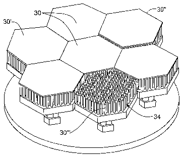
number of which are shown in Fig. 2 as having a hexagonal shape so that they
can be
easily nested. Module 30' is shown in an activated position slightly below the
surface
of the other modules while 30" is shown actuated to a slightly elevated level.
Each
module 30 includes a face sheet which has been removed in the case of module
30"' so
that the high spatial and temporal frequency correction system 34 can be more
easily
seen.
Module 30 is shown in greater detail in Fig. 3 where it can be seen that the
face sheet 32 rests on flexures 36 carried by mirror actuator 38 mounted on
base or
reaction mass 40; face plate 32 may be continuous but need not be. High
spatial and
temporal frequency correction system 34 is in turn mounted on tip-tilt
correction
system 42 which includes three closely clustered tip-tilt actuators 44, 46
with portions
broken away through which can be seen third actuator 48, this too may be
mounted on
a base 50, all of which may be carried on a larger base 52. Although thus far
the
integrated wavefront correction module 30 has been shown as hexagonal in
shape, this
is not a necessary limitation: it may be square as shown in Fig. 4 or it could
be
octagonal, rectangular or any other regular or irregular shape desired to form
the
proper overall mirror surface. Mirror actuators 38 may be XIRE4016's and tip-
tilt
actuators 44, 46, and 48 may be XIRE0750's both obtainable from Xinetics, Inc.
of
Devens, Massachusetts. These tip-tilt actuators would typically have a stroke
of 10 to
40 microns while the mirror actuators would have a stroke of three to six
microns.
Tip-tilt correction system 42 may function as a beam steerer with large tip-
tilt motion,
smaller resolution and low frequency of operation or a fast steering mirror
with small
tip-tilt motion, higher resolution and broader bandwidth. The number of mirror
actuators 38 may be more or fewer depending upon the spatial resolution
desired. The
CA 02579640 2007-03-08
WO 2006/028797 PCT/US2005/030784
9
tip-tilt correction system 42 alternatively may be any suitable drive system
including
electromagnetic actuators, such as voice coils, and stepper motors,
piezoelectric
actuators and the like.
Also, in one preferred embodiment, the high spatial and temporal frequency
correction system may include a transverse electrodisplacive actuator array
disclosed
in U.S. Patent Application No. 10/730,514, entitled Transverse
Electrodisplacive
Actuator Array, by Mark A. Ealey, owned by the same assignee and herein
incorporated in its entirety by this reference and such devices Photonex
#49S3, 144S3,
1024S1 are obtainable from Xinetics, Inc, Devens, Massachusetts.
In a preferred embodiment the tip-tilt correction system may include a multi-
axis transducer as disclosed in U.S. Patent Application No. 10/914,450, filed
August
9, 2004, entitled Inapt=oved Multi-Axis Ti ansducer, by Mark A. Ealey (XIN-
103J)
owned by the same assignee and herein incorporated in its entirety by this
reference.
Such devices X13DOF0510, X13DOF01020 are obtainable from Xinetics, Inc.
Devens, Massachusetts. Each will be explained in turn hereafter.
A transverse electrodisplacive actuator array 148 which may implement the
high spatial and temporal frequency correction system 34 of the integrated
wavefront
correction module 30 includes a plurality of actuators, 150, 152, Fig. 5,
mounted on
support structure 154, which utilizes the strain along the transverse axis
d31, rather
than along the longitudinal axis d33 to expand and contract actuator 150. In
this case,
each actuator includes at least two electrodes, an addressable electrode, 156
and a
common electrode 158. Addressable electrode 156 connects to contact 160 on the
surface 162 of support structure 154, while common electrode 158 connects to
contact
164, on surface 166. In the construction, according to this invention, the
electrodes
CA 02579640 2007-03-08
WO 2006/028797 PCT/US2005/030784
are generally parallel to the direction of expansion and contraction as
opposed to
transverse to it. One advantage is that the interfacial stress is no longer a
factor, as
any separation or crack that occurs is not in series with the force or
displacement, but
rather transverse to it, so that it will not effect the operation of the
device. In addition,
the stroke obtained is no longer dependent on the number of electrodes and
ceramic
layers in the laminate stack, but rather is dependent on the length of
actuator 150, Fig.
5.
Actuator 150, 152, Fig. 5, may be a part of a larger array 148a, Fig. 6, which
includes a number of actuators, 150a, 152a, 172, and 174. Actuators 150a,
152a, 172
and 174 are mounted on support structure 154a, which may be integral with
them.
Their separation may be effected by kerfs or saw cuts, 176, which separate
them in
two dimensions from each other, so they can act as independent elements. Also,
as
shown, each element may have more than just one addressable electrode and one
common electrode. For example, as shown in Fig. 6 with respect to actuator
150a,
there are three addressable electrodes, 180, 182, and 184, which are connected
as a
unit to addressable contact 186. And there may be more than one common
electrode.
For example, there may be four common electrodes 188, 190, 192, and 194
connected
as a unit to common contact 196, which is plated on the mounting surface 198
of
reflective member 200. Reflective member 200 contains on its other side the
reflective surface 202, which is typically a continuous surface. Thus by
selectively
addressing addressable contact 186 one can cause actuator 150a to expand or
contract
and cause a bulge or depression in surface 202 in the locality of actuator
150a.
Similarly when addressable contacts 204, 206, and 208 are selected surface 202
will
be driven in the area local to the associated actuators 152a, 172, 174
respectively, to
CA 02579640 2007-03-08
WO 2006/028797 PCT/US2005/030784
11
form a bulge or a depression depending upon the voltage applied to shape the
optical
wave front being reflected from surface 202. Typically the voltage applied may
have
a quiescent level at 70 volts, so that an increase of 30 volts will drive the
actuator in
one direction to expand or contract and a decease in voltage of 30 volts would
drive it
in the other. Detents 297 of mounting surface 298 are connected to actuators
152a,
154a, 172 and 174 by any suitable adhesive or bonding technique. The actuator
elements have their proximate ends supported by the support structure. Their
distal
ends support the reflective member. The addressable and common electrodes are
spaced apart and generally parallel to each other. The electrodes extend along
in the
direction of the proximate and distal ends of the actuator elements along the
transverse d31 strain axis.
The transverse electrodisplacive actuator array utilizes the transverse strain
of
a ferroic e.g. ferroelectric or ferromagnetic material such as an
electrostrictive
ceramic, lead magnesium niobate (PMN), to produce a scalable, large stroke
microactuator which operates at low voltage and works well in the area of 293K
(room temperature). Using other materials such as tungsten based or strontium
based
materials allows for operation in the area of 125K - 200K and 30K -65K,
respectively. By utilizing the transverse strain component, the
ceramic/electrode
interfacial stress is reduced and the electrical interconnection of a densely
packed
structure is simplified. The electrode interface structure is less sensitive
to machining
tolerances, is more modular in terms of performance and reproducibility, and
is more
cost effective. Fewer laminates are required to form the actuator and the
length is
scaled to meet stroke requirements. Electrical interconnection is accomplished
by
incorporating printed circuit board technology in a common back plane. The
CA 02579640 2007-03-08
WO 2006/028797 PCT/US2005/030784
12
transverse electrodisplacive actuator arrangement provides a scalable
configuration
compatible with up to 107 channels of operation. The problems associated with
the
longitudinal multilayer actuator (electrical interconnects, interfacial
stress, and
precision machining during manufacture) are resolved by incorporating the
transverse
mode of operation. Array 148 may be made of a co-fired interleaved ceramic and
electrode layers or may be made of a single crystal material such as but not
limited to
lead magnesium nitrate, lead zirconate nitrate.
The transverse electrodisplacive actuator array utilizes the transverse
electrostrictive strain of PMN or other ferroic, ferroelectric or
ferromagnetic material
to produce a large stroke, low voltage displacement microactuator without
requiring a
stress sensitive multilayer construction process. Due to the transverse
orientation, the
structural load path is entirely through the ceramic, not through the
electrode/ceramic
interface. Furthermore, the interface stress is greatly decreased since the
dimensional
change in the longitudinal direction is small and inactive material mechanical
clamping or pinning is eliminated. Stroke is attained by adjusting the length,
not by
adding additional layers.
Delineating a monolithic block of ceramic into discrete actuators is
accomplished by standard microsawing techniques. The transverse configuration
is a
fault tolerant design which does not require precision tolerances to prevent
damaging
or shorting out electrodes during manufacture. Electrical interconnection of
electrodes is greatly simplified. Electrical addressing of individual
actuators is
accomplished through the monolithic block which is polished and contains
exposed
electrodes. Printed circuit technology is used to provide the electrical
interconnection
between the discrete addressing actuator channels and the electronic driver.
The result
CA 02579640 2007-03-08
WO 2006/028797 PCT/US2005/030784
13
is a microactuator technology capable of providing sufficient stroke even at
very small
interactuator spacing without the need for multilayer construction or
microscopic
electrical interconnections. The design is easily fabricated without precision
machining and is extremely stress tolerant during electrical activation.
Furthermore,
the design is inherently low voltage which is compatible with hybrid
microelectronic
driver technology. Electrical addressing and interconnection is done at a
common
back plane which lends itself to transverse scaling. The concept provides a
high
performance, scalable microactuator technology using conventional
electroceramic
fabrication and processing technology.
Although in Fig. 6 the transverse electrodisplacive actuator array was shown
having its common electrode 196 carried by the mounting surface 198 of
reflective
meinber 200 this is not a necessary limitation. As shown in Fig. 7, in array
148b,
reflective member 200a may be constructed without a contact on its mounting
surface
198a and instead the common contacts 196a for the common electrodes may be
established at surface 199. In that way the array including actuators 150a,
152a, 172
and 174 may be fully powered and tested before the reflective member, 200a is
attached by bonding or adhesive.
The entire array, both the support structure 154a, and the actuators 150a,
152a,
172 and 174 may be made by effecting cuts in two mutually perpendicular
directions
down into a block of suitable material ferric ceramic with the cuts or kerfs
effecting
the separation of the actuators into the individual elements. There may just a
few cuts,
210, and resulting actuators, 212, as shown with respect to array 148c, Fig. 8
or there
may be many cuts, 214, resulting in many actuators, 216, as shown with respect
to
array 148d, Fig. 9. The interconnection of transverse electrodisplacive
actuator array
CA 02579640 2007-03-08
WO 2006/028797 PCT/US2005/030784
14
148e, Fig. 10 having a multiplicity of actuators 220, carried by support
structure 222,
may be made by forming the contacts 186a and 196a, Fig. 7, on the lower
surface 223,
Fig. 10, using solder pads, 224, on top of which is fastened a socket grid
array, 226, to
receive the pin grid array, 228 carried by flex cable 230.
The advantageous modularity of the transverse electrodisplacive actuator array
according to this invention is displayed in Fig. 11, where it can be seen that
a number
of smaller transverse electrodisplacive actuator arrays 220, Fig. 10 are
combined in
Fig. 11, to form a larger assembly, 232, to accommodate a much larger
reflective
member, 234 which also may be a continuous surface. Now all of the flex cables
represented by a single cable, 236, are connected to driver circuit, 140b,
which is
driven by microprocessor 142b. With selected programming of driver circuit
140b by
microprocessor 142b, it is possible to have an unenergized active aperture as
shown in
Fig. 12A; a single actuator energized to about 250nm as shown in Fig. 12B,
every
third actuator energized as shown in Fig. 12C or every other actuator
energized as
shown in Fig. 12D. Multiple modules comprising 441 actuators or more having
one-
millimeter spacing arranged in 21 by 21 arrays have been demonstrated. Mirror
deformations have been obtained, which are .25 micrometers at 100 volts and
are
repeatable to V1000rms. The average capacitance for each actuator may be 30nf
while the average stroke maybe 250nm.
A multi-axis transducer 310, Fig. 13, which may implement the tip-tilt
correction system 42 of the integrated wavefront correction module 30 includes
addressing conductors 312, 314 and 316 and common conductor 318. Transducer
310
is formed of a plurality of layers typically numbering in the tens or
hundreds. The
layers are separated by electrodes, alternately common electrodes and
addressing
CA 02579640 2007-03-08
WO 2006/028797 PCT/US2005/030784
electrodes. Layers 320 are made of a ferroelectric electrodisplacive material,
such as
electrostrictive, piezoresistive, piezoelectric, or pryoresistive materials
e.g. lead
magnesium nitrate, lead zirconate titanate. Disposed between alternate layers
are
addressing electrodes 322 with the common electrodes 324 being interstitially
alternately disposed These combinations of layers and electrodes form
capacitors
which may be viewed as mechanically in series and electrically in parallel.
The layers
320 may be very thin, for exainple, 4 mils as compared to the prior art
longitudinal
walls which are 40 to 100 mils thick, those prior art devices required a 1
000v to
2500v voltage supplies where as this structure using 4 mil layers would
require only
approximately 100 volts. Further when this transducer is operated as an
actuator it
will have greater displacement because it has a greater number of layers and
displacement is a function of the number of layers squared times the electric
field:
D ,z:~ N2x E
(1)
where
E=Vlt (2)
and where V is the voltage and t is the thickness.
When operated as a sensor transducer 310 performance is also improved
because the co-firing which results in a monolithic integrated structure
increases the
stiffness of the device, and therefore gives it a greater sensitivity to any
applied forces.
F ~'cVA (3)
where p is density, A is area and Y is Young's Modulus. The higher the Young's
CA 02579640 2007-03-08
WO 2006/028797 PCT/US2005/030784
16
Modulus the stiffer the device and therefore the greater will be the
sensitivity of the
device as a sensor and the greater will be the force developed by the device
as an
actuator. Co-firing also produces an integrated structure wherein the
electrodes, layers
and even the addressing and common conductors are an integral part of the
package.
The greater stiffness also increases the bandwidth of the transducer
1 rk
21l (4)
where k is stiffness, m is mass and fr is the natural frequency and
Ya
k=-
Z
(5)
where 1 is the length of the transducer. Co-firing is a well known fabrication
process
which involves removing carbon from the green body during binder burnout and
densifying the ceramic during sintering with the result being a monolithic
multilayer
stack. For further information see Ceramic Processinz and Sinterin.g, M.N.
Rahamen,
Principles of Ceramic Processinz, James S. Reed.
Each addressing electrode 322 includes two or more sections. In Fig. 13, the
addressing electrodes 322 include three sections 328, 330 and 332 but fewer,
two, or
more 6, 10, 50, 100, 500 or any number may be used limited only by the
manufacturing tolerances and the resolution desired. Transducer 310 is
typically
cylindrical in form and circularly symmetrical about centerline C/L and may
have a
central hole 326 to improve its performance. Each section 328, 330, 332 in
each
addressing electrode 322 forms a set with a corresponding sections in the
other
addressing electrodes. That is to say, all of the sections 328 in all of the
addressing
CA 02579640 2007-03-08
WO 2006/028797 PCT/US2005/030784
17
electrodes 322 which are connected by addressing conductor 312 form a set as
do all
the sections 330 interconnected by addressing conductor 318 and all of the
sections
332 interconnected by addressing conductor 316. These sets are referred to as
334,
336, and 338, respectively.
When transducer 310 is operated as a actuator an electric field is created in
layers 320 by applying a voltage across the pairs of addressing and common
electrodes
through addressing conductors 312, 314 and 316 and common conductor 318. If
all of
the applied voltages are equal, a displacement is generated in the Z axis
longitudinally, if unequal voltages are applied then the sets 334, 336, 338 of
sections
328, 330, and 332 will undergo different displacements and there will be a
tilting,
imposing a motion in the X and Y axes as well. Each of sections 328, 330 and
332 on
each of addressing electrodes 322 are electrically isolated from each other,
such as by
insulating portions 340, 342 and 344.
In order to ensure that the addressing conductors 312, 314 and 316 touch only
addressing electrodes, not common electrodes, and that common conductor 318
touches only common electrodes, not addressing electrodes, the addressing and
common electrodes are suitably configured with recesses. For example, each of
common electrodes 324, Fig. 14, is recessed from the edge 352 of the stack of
layers
320 so that it cannot electrically connect to addressing conductor 316 which
is
electrically interconnected to each of the addressing electrodes 322, such as
at
terminals 354. Similar recessing is done of the addressing electrodes to avoid
contact
with all but the common conductor.
This construction can be seen in more detail in Fig. 15, where three layers
320a, 320b and 320c are shown in exploded isometric view. Addressing electrode
CA 02579640 2007-03-08
WO 2006/028797 PCT/US2005/030784
18
322a includes three sections 328a, 330a and 332a electrically separated by
insulators
340a, 342a, and 344a. A portion of section of 330a is recessed as at 360, in
fact only
one recess is needed where there is typically only one common conductor, but
for ease
of manufacturing and assembly recesses are often provided in each of the
sections as
shown in phantom at 362 and 364. Common electrode 324a includes three recesses
366, 368, and 370 to be sure that there is no contact with addressing
conductors 312,
314, and 316, respectively. The next layer 320c includes an addressing
electrode 322c
having three sections, 328c, 330c, and 332c with insulators 340c, 342c, and
344c and
recesses 360c, 362c, and 364c.
The transducer of this invention may be easily fabricated by fabricating a
number of ferroelectric layers 400, Fig. 16, on which have been developed
common
electrodes 402 and fabricating a number of ferroelectric layers 404 on which
have
been developed a number of addressing electrodes 406, Fig. 17. Hundreds of
these
layers 400 and 404 are then stacked alternately and in registration following
wllich the
individual stacks of addressing and common electrodes are cut from the
substrate and
co-fired to form a number of transducers according to this invention.
Although thus far the transducer has been referred to as operating as either a
sensor or actuator it may function as a co-located combination sensor and
actuator.
Such a co-located sensor actuator 410, Fig. 18, is constructed in the same way
as the
transducer shown in Figs. 13, 14 and 15, except that one group of addressing
electrodes is designated the sensor group 412, and the other group of
addressing
electrodes is designated as the actuator group 414. There may still be one
common
conductor 416 but now there are addressing conductors 418, 420 and 422 , one
for
each of the addressing electrodes in sensor group 412 and separate addressing
CA 02579640 2007-03-08
WO 2006/028797 PCT/US2005/030784
19
conductors 424, 426, 428 for the addressing electrodes in the actuator group
414.
The same co-location sensor-actuator function can be obtained using a
different confirmation as shown in Fig. 19, where transducer 430 is shown
having
each of its addressing electrodes 432 separated into a number of sections
which are
alternately actuator sections 434 and sensor sections 436 disposed on the same
layer.
Thus each of the addressing electrodes has an alternating pattern of actuator
and
sensing sections which form three sets of sensing sections interstitially
disposed with
respect to three sets of actuator sections. In both transducers 410 and 430 in
Figs. 18
and 19, the result is a co-located integrated and monolitliic, co-fired,
transducer which
can operate both as a sensor and as an actuator to provide both displacement
and force
sensing. Alternatively, the device in Fig. 18 could have every other capacitor
plate act
as an actuator and the interstitial ones act as a sensor, instead of having
two distinct
groups as shown.
With the configuration shown thus far, where the transducer is shaped as an
elongated cylinder, as shown in Fig. 20, where the length L is much greater
than the
diameter D, the better performance is along the longitudinal access or the d33
axis.
However, the transducer of this invention works just as well when d31 is the
preferred
axis, if the aspect ratio is reversed so that the diameter D, Fig. 21, is much
greater than
the length L.
As is well know in the art, sensing and control circuits, such as disposed in
the
instrument and control packages 28, Fig. 1, include sensors and circuits for
sensing
high spatial and temporal frequency errors and tip-tilt errors in the incident
wavefronts
on the telescope system, for example e.g. on face plates 32. These circuits,
which
form no part of this invention, develop compensation signals which are then
applied to
CA 02579640 2007-03-08
WO 2006/028797 PCT/US2005/030784
the tip-tilt correction system in high spatial and temporal frequency
correction system
to correct for those errors. The interconnection of those circuits can be done
in a
number of ways. Base or reaction mass 40b, Fig. 22, can include a framework
500
having a space 502 for accommodating the wire interconnects 504 from high
spatial
and temporal frequency correction system 34b which then passes through a
central
hole 506 in tip-tilt correction system 42b whether it be a plurality of
discrete actuators
or a multi-axis transducer and then through a similar hole 508 in base 52b.
Interconnect wires 510 join them in cable 512 passing through hole 508.
Alternatively, integrated wavefront correction module 30c, Fig. 23, may
include a flat
cable 514 which interconnects through the contacts on base 40c for each of the
actuators 38, and then is covered by a protective insulating layer 516 to
which may be
mounted the tip-tilt correction system 42c. Once again it can be driven by
wire
connections 510a, which are lead througll hole 508a to cable 512a.
Whether the tip-tilt correction system 42d, Fig. 24, is a plurality of
discrete tip-
tilt actuators, such as 44, 46, and 48 shown in Fig. 3, or a single multi-
access actuator
as shown in Fig. 13, it is advantageous to have the force train application
points
clustered together proximate the center of the optical surface, which is the
fulcrum for
the tip-tilt motion, in order to gain the most motion amplification for the
tip-tilt
motion of the mirror. In Fig. 3 the force train application point axes 45 and
47 of
actuator 44, and 46 and the axis of actuator 48, not shown, are close to the
center of
rotation axis 49 of mirror surface 32. Using the multi-axis transducer of Fig.
13, the
force train application point axes are close together and proximate the center
of the
optical surface as well, but this is not a necessary limitation. For example,
integrated
wavefront correction module 30d, Fig. 24, includes three discrete tip-tilt
actuators
CA 02579640 2007-03-08
WO 2006/028797 PCT/US2005/030784
21
44d, 46d, and 48d. Spaced well apart from the rotation center axis 49d which
passes
through the center of hole 508d on base 52d and through the center of rotation
53d of
mirror surface 32d. But each of these tip-tilt actuators 44d, 46d and 48d
includes an
arm 518, 520 and 522 which extends from the top of its associated actuator
towards
the center line 49d. There the force train application points 524, 526 and 528
have
their axes 45, 47 and 51 respectively, clustered together and close to the
center axis
49d, thereby garnering the mechanical advantage of being close to the fulcrum
point,
center of rotation 53d, to provide motion amplification for the tip-tilt
motion. This is
but one example of many different mechanical advantage systems that could be
used
for this purpose.
Altliough thus far the integrated wavefront correction module has been shown
with the high spatial and temporal frequency correction system being mounted
on the
tip-tilt correction system so that the tip-tilt correction system actually
moves the entire
high spatial and temporal frequency correction system in turn applying the tip-
tilt
correction to optical surface 32d, this is not a necessary limitation. The two
correction
systems could be applied in parallel as shown in Fig. 25 where integrated
wavefront
correction module 30e includes tip-tilt correction system 42e having three
spaced
apart tip-tilt actuators 44e, 46e and 48e which support optical surface or
face plate
32e. Suspended from faceplate 32e is high spatial and temporal frequency
correction
system 34e so that while high spatial and temporal frequency correction system
34e is
indeed still moved by tip-tilt correction system 42e it is not in series with
it. For tip-
tilt correction system 42e doesn't move faceplate 32e through high spatial and
temporal frequency correction system 34e but independently and so does the
high
spatial and temporal frequency correction system 34e. This requires an
extremely
CA 02579640 2007-03-08
WO 2006/028797 PCT/US2005/030784
22
light weight high spatial and temporal frequency correction system 34e to be
carried
by face plate 32e or there could be a stiffening layer as shown in 33e, shown
in
phantom, to provide the necessary stiffness.
Although specific features of the invention are shown in some drawings and
not in others, this is for convenience only as each feature may be combined
with any
or all of the other features in accordance with the invention. The words
"including",
"comprising", "having", and "with" as used herein are to be interpreted
broadly and
comprehensively and are not limited to any physical interconnection. Moreover,
any
embodiments disclosed in the subject application are not to be taken as the
only
possible embodiments.
Other embodiments will occur to those skilled in the art and are within the
following claims:
What is claimed is: