Note: Descriptions are shown in the official language in which they were submitted.
CA 02579818 2007-03-08
WO 2006/034017 PCT/US2005/033129
1
FIELD DEVICE INCORPORATING CIRCUIT CARD
ASSEMBLY AS ENVIRONMENTAL AND EMI/RFI
SHIELD
FIELD OF THE INVENTION
The present invention relates to electronic
field devices, such as process transmitters, that are
used to monitor industrial processes. More
particularly, the present invention relates to
electronic field devices used in industrial process
environments that may have high electromagnetic
interference (EMI).
BACKGROUND OF THE INVENTION
Generally, electronic field devices (such as
process transmitters) are used to monitor the operation
of industrial processes such as those in oil
refineries, chemical processing plants, paper
processing plants, biotechnology plants, pharmaceutical
plants, food and beverage plants, and the like. Process
transmitters for monitoring an industrial process may
measure pressure, flow rate, fluid or material level in
a tank, temperature, vibration, and the like.
Additionally,, such field devices may include analytical
electronics, diagnostic electronics, or other process
monitoring electronic devices, or even electronic,
hydraulic or pneumatic actuator devices used for
industrial process control.
Process transmitters are typically positioned
within the processing plant in locations where liquids,
dust and humidity and various industrial contaminants
may be present. In some environments, process liquids
CA 02579818 2007-03-08
WO 2006/034017 PCT/US2005/033129
-2-
such as acid solutions or base solutions can be
present. Liquids may also include spray from hoses used
to clean plant equipment. Liquids can drip, splash or
spray onto the process transmitter and its electrical
connections. Additionally, dust, humidity, and liquids
in the environment may contaminate and degrade the
electrical connections to and within the process
transmitter.
Transmitters that include circuitry
disposed in a sealed housing and protected by an
outer cover are known in the art. It is also known
to include one or more actuatable switches for
modifying a parameter of the circuit, such as a zero
or span setting. Typically, the one or more switches
or the field wiring terminals are accessible only
after removal of the outer transmitter cover.
Unfortunately, removal of the outer cover exposes
the electronics within the transmitter housing to
contaminants and electromagnetic and radio frequency
interference. One technique for maintaining EMI
protection for electronics within the transmitter
housing includes an electrically conductive inner cover'
disposed within the transmitter housing and in
frictional contact with electrically conductive walls
of the housing to reduce the effects of EMI when the
outer cover is removed. One example of a process
transmitter with an inner conductive cover is shown and
described in U.S. Patent No. 5,353,200 issued to Bodin
et al. and entitled "PROCESS TRANSMITTER WITH INNER
CA 02579818 2008-01-16
-3-
CONDUCTIVE COVER FOR EMI SHIELDING" issued October 4,
1994.
There is an ongoing need in the art for industrial
process transmitter housing configurations with
improved humidity and environmental contamination
robustness as well as efficient EMI/RFI filtering
capabilities. Embodiments of the -present invention
provide solutions to these and other problems, and
offer other advantages-over the prior art.
SUMMARY
A field hardened. industrial device is
described. A housing of the field hardened
industrial device has electrically conductive walls
surrounding a cavity with an open end. An
electronics assembly is adapted to fit within the
cavity. A portion of the electronics assembly is a
circuit card assembly, which is a multi-layered
printed wiring board with pass-through electrical
connections and an embedded ground plane electrically
coupled to the housing to shield the electronics
assembly from electromagnetic interference and to
provide environmental protection to the electronics
assembly-
According to one aspect of the invention
there is provided a field hardened industrial device
comprising:
a housing having electrically conductive walls
surrounding a cavity having an open end;
an electronics assembly adapted to fit within the
cavity; and
a circuit card assembly adapted for electronic
coupling to the electronics assembly, the circuit
CA 02579818 2008-01-16
- 3a -
card assembly comprising a multi-layered printed wiring
board with pass-through electrical connections and an
embedded ground plane electrically coupled to the housing
to shield the electronics assembly from electromagnetic
interference and to provide environmental protection to the
electronics assembly.
According to a further aspect of the present
invention there is provided a circuit card assembly for field
hardened industrial devices deployed in industrial process
environments comprising:
a multi-layered printed wiring board with pass-through
electrical connections sized to fit within a cavity of a device
housing; and
a ground plane embedded within the printed wiring board and
extending substantially a full extent of the multi-layered
printed wiring board, the ground plane electrically coupled to
the device housing to shield electronics within the device
housing from electromagnetic interference and to provide
environmental protection to the electronics.
According to another aspect of the invention there
is provided a transmitter for use in an industrial process
comprising:
a housing having electrically conductive walls surrounding a
cavity having an open end;
an electronics assembly adapted to fit within the cavity; and
a circuit card assembly adapted for electronic coupling to
the electronics assembly, the circuit card assembly comprising
a multi-layered printed wiring board with pass-through
electrical connections and an embedded ground plane coupled to
the housing to shield the electronics assembly from
electromagnetic interference and to provide environmental
protection to the electronics assembly.
CA 02579818 2008-01-16
- 3b -
In one embodiment, the multi-layered printed wiring
board with pass-through electrical connections is sized to fit
within the cavity of the device housing. A ground plane embedded
within the printed wiring board extends substantially a full
CA 02579818 2007-03-08
WO 2006/034017 PCT/US2005/033129
-4-
extent of the multi-layered printed wiring board.
The ground plane is electrically coupled to the
device housing to shield electronics within the
device housing from electromagnetic interference and
to provide environmental protection to the
electronics.
BRIEF DESCRIPTION OF THE DRAWINGS
FIG. 1 is a simplified block diagram of a
field device according to an embodiment of the
present invention.
FIG. 2 is a cross-sectional view of a field
device, including a circuit card assembly according
to an embodiment of the present invention.
FIG. 3 is an expanded cross-sectional view
of a portion of the circuit card assembly according
to an embodiment of the present invention.
FIG. 4A is a simplified top view of a
printed circuit substrate including a plurality of
circuit card assemblies according to an embodiment of
the present invention.
FIG. 4B is an expanded top view of one of
the circuit card assemblies of FIG. 4A.
FIG. 5A is an expanded cross-sectional view
of a blind via through a circuit card assembly
according to an embodiment of the present invention.
FIG. 53 is a simplified block diagram of a
top view of a ground plane and via interconnection
layer taken along dotted-line 460. in FIG. 5A
according to an embodiment of the present invention.
CA 02579818 2007-03-08
WO 2006/034017 PCT/US2005/033129
-5-
FIG. 6A is an expanded cross-sectional view
of a via through a circuit card assembly according to
an embodiment of the present invention.
FIG. 6B is a simplified block diagram of a
top view of a ground plane and via interconnection
layer taken along dotted-line 460 in FIG. 6A
according to an embodiment of the present invention.
While the above-identified illustrations
set forth embodiments of the present invention, other
embodiments are also contemplated, some of which are
noted in the discussion. In all cases, this
disclosure presents the illustrated embodiments by
way of representation and not limitation.
DETAILED DESCRIPTION
The present invention is directed to a
field hardened industrial device, such as a process
transmitter, preferably utilizing a single
compartment electrical housing that maintains EMI
protection and environmental protection even with the
outer transmitter cover removed. As used herein, the
phrase "field hardened industrial device" refers to a
device with a housing that is sealed against
environmental contamination. In a preferred
embodiment, in addition to the housing being sealed
against the environmental contamination, the
electronics are additionally sealed against
environmental contamination, as well as
electromagnetic and radio frequency interference. In
a preferred embodiment, the environmental seal
CA 02579818 2007-03-08
WO 2006/034017 PCT/US2005/033129
-6-
provided by the circuit card assembly is a hermetic
seal. As used herein, the term "hermetic" refers to
a seal having a leak rate that is less than
approximately 5x10.8 std cc/sec He (0.00000005 cubic
centimeters of Helium per second given at one
atmosphere of pressure),. Additionally, as used
herein, the term "EMI" or "Electromagnetic
Interference" refers to interference from
electromagnetic radiation containing primarily
electrostatic (electrical field or E-field) energy at
a frequency between 0 Hz (DC) and approximately 10
GHz.
The present invention incorporates a
circuit card assembly (CCA) that serves as an
electrical connection from the device electronics to
the field wiring and to the local operator interface
(LOI) or LCD display on the field wiring side of the
device. Moreover, the CCA is provided with an
embedded ground plane electrically connected to the
electrically conductive device housing to provide EMI
shielding. The ground plane of the CCA effectively
divides the device housing into two "Faraday cages"
and serves as both an environmental shield and EMI
barrier.
In general, a Faraday cage is an enclosure
formed from conducting materials designed to prevent
the passage of electromagnetic waves, either by
containing them within or excluding them from its
interior. Process transmitters are typically formed
CA 02579818 2007-03-08
WO 2006/034017 PCT/US2005/033129
-7-
from conductive metal and are themselves Faraday
cages. Effectively, the exterior surface of the
transmitter housing serves as an equipotential
surface having essentially the same electrical
potential at every point. The principle of the
Faraday cage is that a charge on a charged conductor
resides only on its exterior surface. If there is no
electrical charge inside of the structure, then by
Gauss' law and the divergence theorem, there is no
electrostatic field inside the equipotential surface,
even if the structure is exposed to an external
field.
Within the process industry, such
conductive structures are utilized to eliminate
electric fields within the structure so as to protect
electronics from undesired electromagnetic signals.
Ideally, electric fields and radio frequencies cannot
penetrate the Faraday cage to affect the electronics.
It should be appreciated that the Faraday cages of
the present invention are not perfect because the
housing material (though conductive) is not a perfect
conductor, and because the enclosure is provided with
an opening for wiring to enter the housing. In
addition to moisture and other contaminants, radio
frequency interference (RFI) and electromagnetic
interference (EMI) can be coupled (conducted) into
the electronics within the housing via the wires.
Nevertheless, as used herein, the term "Faraday cage"
refers to an electrically conductive structure having
CA 02579818 2007-03-08
WO 2006/034017 PCT/US2005/033129
-8-
sufficient Faraday cage properties to shield the
enclosed volume from external electromagnetic
interference and radio frequency interference.
Figure 1 illustrates a simplified diagram
of a process transmitter system 100 according to an
embodiment of the present invention. Process
transmitter 102 is coupled to process pipe segment
104 in order to measure a parameter or process
variable associated with a fluid contained within the
pipe section 104. The transmitter 102 is coupled to
control center 106 via a field wiring 108. In
general, the field wiring includes both power/ground
cabling and a communications link. The field wiring
108 may include two or more wires. In an alternative
embodiment, the field wiring 108 provides power and
ground connections, but communication between the
transmitter 102 and the control center 106 occurs via
wireless communications link (not shown).
In general, transmitter 102 includes a housing
110 with a cover 112. A housing 110 is coupled to the
pipe segment 104 via a sealed base 114, which may
include a coupling flange or other attachment
mechanism provided by a customer for a specific
installation. A wiring conduit 116 is provided on the
housing body 110 to provide an access opening for the
field wiring 108 to enter the housing 110 for
connecting electronics within the transmitter housing
110 to the control center 106.
CA 02579818 2007-03-08
WO 2006/034017 PCT/US2005/033129
-9-
A circuit card assembly (CCA) 270 shown in FIG.
2 and discussed below is disposed within the
transmitter housing 202, and is provided with an
embedded ground plane, which contacts the transmitter
housing at several points to complete a ground
connection. The CCA isolates electronics disposed
below the CCA in the transmitter housing 202 from
electromagnetic interference and environmental
contaminants, if the transmitter cover 208 is
removed.
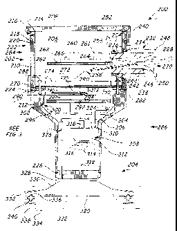
Figure 2 is a cross sectional view of a
single compartment transmitter housing according to
an embodiment of the present invention. In this
example, the transmitter 200 is a pressure
transmitter 200 for measuring a fluid pressure in a
pipe or vessel of an industrial process. However,
the transmitter 200 may include any type of
industrial sensor.
The transmitter 200 includes a transmitter
housing 202 coupled to a base portion 204 defining an
enclosure 206 with an opening. A releasable cover
208 is sized to fit over the opening to seal the
enclosure 206 from the environment. The housing 202
includes an upper portion 210 and a 'lower portion
212. The upper portion 210 is provided with threads
214 on an outer surface sized to mate with threads
216 on an inner surface of the cover 208.
Additionally, a recess 218 sized to receive an o-ring
seal 220 is preferably provided in the outer surface
CA 02579818 2007-03-08
WO 2006/034017 PCT/US2005/033129
-10-
of the upper portion 208. An overhang portion 222 of
the cover 208 compresses the o-ring seal 220 to
isolate the enclosure 206 from the environment.
Generally, the upper portion 210 is coupled to
the lower portion 212 via weld joint 224 or other
conductive means. The lower portion 212 is coupled
to the base portion 204 via weld joint 226 or other
conductive means.
Field wires 228 extend through wire opening 230
into the upper portion 210 of the housing 202. A
conduit connection 232 having a body portion 234 and
coupling portions 236 and 238. The body portion 234
is sized to mate with a corresponding recess 240
provided in an outside surface of the upper portion
210 adjacent to the wire opening 230. Coupling
portion 236 is provided with threads adapted to mate
with a coupling nut 242 within the enclosure 206. A
gasket 244 is disposed over the coupling portion 206
between the coupling nut 242 and the inner surface of
the upper portion 210 to seal the enclosure 206
around the opening 230. Alternatively, a conduit or
entry spud or a preformed receptacle can be welded or
permanently attached to the housing directly.
The field wires 228 are positioned within a wire
connector 246, and connector nut 248 is threadably
attached to coupling portion 238 to fix the field
wires 228 in position. In particular, as the
connector nut 248 is tightened onto the coupling
portion 238, flange portions 250 of the wire
CA 02579818 2007-03-08
WO 2006/034017 PCT/US2005/033129
-11.-
connector 246 are forced against the inner surface of
the coupling portion 238 causing the wire connector
246 to clamp the field wires 228 into position.
Within the enclosure 206, the field wires 228
are broken out into individual leads, including a
ground lead 252 coupled to a ground lug 254 and a
power lead 256 and a signaling lead 258 coupled to
spring loaded electrical contacts 280 provided on
coupling board 270. The coupling board 270 is
readily accessible to an operator in the field upon
removal of cover 208. The Local Operator Interface
(LOI) board 262 connects to the coupling board 270
and provides easy access to field device elements
that may need to be accessed, including the span
setting push button 264 and the zero setting push
button 266 for resetting the transmitter 200, as well
as the alarm switch 260 and the write protect switch
261.
In this embodiment, the LOI board 262 is
fixed within the upper portion 210 of the transmitter
housing 202 via screws 268 and is separated from the
circuit card assembly or coupling board 270 by
standoffs 272 and by clamping ring 274. Clamping
ring 274 mates with coupling board 270, which in turn
mates with seal 290. Threaded fasteners 288 extend
through the clamping ring 274, the coupling board 270
and through seal 290 and into the lower portion 212
of housing 202, fixing the coupling board 270 in
place. In general, fasteners 288 may include bolts,
CA 02579818 2007-03-08
WO 2006/034017 PCT/US2005/033129
-12-
screws, or other threaded fastening elements.
Alternatively, the fasteners 288 need not be
threaded, and may include fasteners such as pins,
drive screws and the like.
A radio frequency interference filter (RFI
filter) 278 located on the coupling board 270
capacitively couples .the pins of the field wiring
connector 280 to the ground plane 350 and hence to
the transmitter housing 202. The RFI filter 278 is
adapted to filter radio frequency interference, which
may be coupled in on the field wiring 228, and
generally to protect the electronics assembly from
line conducted interference.
Finally, the circuit card assembly (CCA or
coupling board) 270 is preferably comprised of a
multi-layered printed wiring board (PWB) that is
plated on its outer circumferential edge with a
conductive layer 282. Generally, the PWB is formed
from an insulating material, such' as ceramic,
plastic, and the like, on which wire traces and
electrical interconnections can be formed.
As will be discussed in greater detail below,
the coupling board 270 includes an embedded ground
plane 350, which extends substantially the entire
diameter of the coupling board 270 and which couples
to the conductive layer 282. The embedded ground
plane 350 is a. planar layer disposed within the CCA
270 and extending substantially the entire diameter
of the CCA 270. The embedded ground plane 350 is
CA 02579818 2007-03-08
WO 2006/034017 PCT/US2005/033129
-13-
formed from a conductive material (such as copper),
and is intended to electrically connect with the
conductive walls of transmitter housing 202 to shield
the electronics assembly from EMI. In general, the
electrical connection between the ground plane 350
and the housing 202 may be completed through the
conductive layer 282, via fasteners 288, through the
conductive edge layer 282, or by other means. In one
embodiment, seal 290 is electrically conductive and
the ground path is established through the seal 290.
By electrically coupling the ground plane to the
housing 202, the CCA 270 effectively divides the
housing 202 into two Faraday cages (Faraday cage 284
above the CCA 270 and Faraday cage 286 below the CCA
270).
In this embodiment, within the lower portion 212
of the housing 202, the CCA 270 is coupled to a
transmitter circuit card assembly (CCA) 292 via a
flexible circuit 294. Connector 296 couples the
flexible circuit 294 'to the CCA 270. Connector 297
couples the other end of the flex circuit 294 to the
transmitter CCA 292. A heat sink 295 is preferably
fixed between the CCA 270 and the flex circuit 294 to
provide a thermal conduction path for any heat
generating components located on flex circuit 294.
The transmitter CCA 292 is seated within a
cup 298, which has a hook 300 adapted to mate with a
recess 302 provided in the lower portion 212. The
hook 300 secures the cup 298 in position within the
CA 02579818 2007-03-08
WO 2006/034017 PCT/US2005/033129
-14-
lower portion 212. A connector 304 couples flexible
circuit 306 to the low-level transmitter CCA 292,
which in turn connects to the pressure sensor 308 via
contact pins 310.
In the embodiment shown, the pressure sensor 308
includes a glassed feed through 312 for the
electrical contact pins 310. The glassed feed
through 312 extends to the environmentally sealed
sensing diaphragm 314 adjacent to the oil filled
cavity 316 within the sensor 308. An oil filled tube
318 connects the sensor 308 to the cavity 320
adjacent to the isolating diaphragm 322, which is
coupled to the process.
A fill tube 324 is provided on sensor 308 to
backfill the oil filled cavity 316, tube 318 and
cavity 320 to the desired level. An air filled tube
326 connects the sensor 308 to a vent to atmosphere
328, which allows the transmitter to measure gage
pressure.
Finally, the base 330 is preferably coupled to
the process by a clamp 332 and flange 334 provided by
the customer to mate with their particular
implementation. Recesses 336 and 338 provided in the
base 330 and the flange 334 are sized to receive
gasket 340, which seals the base 330 to the flange
334.
In general, it should be understood by a worker
skilled in the art that the present invention may be
used with any type of sensing element, not just the
CA 02579818 2007-03-08
WO 2006/034017 PCT/US2005/033129
-15-
gage pressure sensor shown. In particular, the CCA
270 of the present invention may be used with any
process transmitter, provided the skin depth of the
ground plane embedded within the CCA 270 is of a
thickness sufficient to effectively isolate the
electronics from EMI, which may be coupled in on the
field wiring 228 or which may be introduced from the
operating environment when the outer cover 208 is
removed. Additionally, the present invention may be
used with any field-hardened industrial device,
including remote meters, wireless gateways, remote
monitoring units, industrial process transmitters,
and the like.
FIG. 3 illustrates an expanded cross-sectional
view of the CCA 270 and a portion of the assembly
where the upper portion 210 and lower portion 212 of
the housing 202 are welded by weld joint 224. As
previously discussed, the edge of the CCA 270 is
plated with a conductive layer 282. In general, the
CCA 270 is a multi-layered substrate, including an
embedded ground plane 350 sandwiched between upper
layer 352 and lower layer 354. Generally, the upper
and lower layers 352 and 354 and ground plane 350 are
portions of a multi-layer printed wiring board (PWB).
Generally, the exposed planar surfaces 360 and 362
are water resistant. However, during the fabrication
process, holes are drilled and edges of the substrate
are cut to form the PWB 270. These exposed edges
have exposed fibers, which can act as wicks to draw
CA 02579818 2007-03-08
WO 2006/034017 PCT/US2005/033129
-16-
moisture into the substrate layers 360 and 362. To
prevent this, the edge of the PWB 270 is plated with
a conductive layer, such as copper or tin, that also
serves as a diffusion barrier to humidity and
contaminants. Additionally, each via or hole is
plated.
As previously discussed, threaded fastener 288
extends through the clamping ring 274, through the
CCA 270, through gasket 290 and into the lower
portion 212. The opening through the CCA 270 that
accepts threaded fastener 288 is also plated by a
conductive layer 356 to prevent moisture from
entering the board through the opening. Depending on
the specific implementation, the ground plane 350 may
be etched away from the plated layer 356 of the holes
to prevent a short to ground via the threaded
fastener. Alternatively, the plated layer 356 may
provide a path to the ground for the ground plane
350, depending on the specific implementation.
As previously discussed, the threaded fastener
288 frictionally mates with the conductive lower
portion 212 (and/or upper portion 210 of the housing
202 and the PWB conductive layer 364, and
electrically connects to the ground plane 350 via
conductive layer 356 or conductive layer 282 to
shield the sensor electronics (such as sensor 308 in
FIG. 2) from EMI.
In one embodiment, the seal 290 is an electrical
insulator, which prevents the CCA 270 from
CA 02579818 2007-03-08
WO 2006/034017 PCT/US2005/033129
-17-
frictionally mating with the housing 202. Clamping
ring 274 frictionally mates with a conductive trace
on the outer surface of the CCA 270, while threaded
fasteners 288 ultimately provide the ground path to
the housing 202. If seal 290 is electrically
conductive (such as with commercially available EMI
gaskets), the ground path could be made through seal
290 instead of through threaded fastener 288.
FIG. 4A is a top plan view of a substrate 400 on
which multiple PWBs 402 have been produced. In
general, the multi-layered substrate 400 is
manufactured, then the individual PWBs 402 are
routed, drilled, etched and plated to produce the
completed circuit card. Specifically, the outline of
the PWB 402 is cut through the board, such as route
channel 404. The route channel 404 is not
continuous. The PWB 402 is cut out, except for small
tab portions 406, which secure the PWB 402 in the
plane of the substrate 400.
Fastener openings 408, electrical connection
vias 410, and component thru-holes 416 are formed in
the PWB 402. The edge of the board (channel 404) and
the openings 408, vias 410, and component thru-holes
416 are coated with a conductive layer 412. To
assist 'an operator in completing the installation
using the PWB 402, connector outlines and text may be
printed on the PWB 402 as indicated by reference
numeral 414.
CA 02579818 2007-03-08
WO 2006/034017 PCT/US2005/033129
-18-
FIG. 4B illustrates an expanded top view of a
PWB 402, such as those shown in FIG. 4A. Later,
after assembly of the components to the PWB 402, the
PWB is referred to as the circuit card assembly or
CCA 402. After component assembly, the CCA 402 is
broken out from the substrate 400, leaving tab
portion 406, which is not coated with the conductive
layer 412 on its tip. The electrical connection
between the conductive layer 412 and the electronic
device or transmitter housing (such as transmitter
housing 202 in FIG. 2) is sufficient to provide EMI
shielding for electronics in the housing. Moreover,
relative to the circumferential area that is coated
by the conductive layer 412, the small exposed area
of the tab portion 406 does not present a significant
moisture "wicking" problem and could easily be coated
over with epoxy or the like to further improve the
moisture resistance.
For complete protection against the moisture
"wicking" problem, the channel 404 in the PWB panel
can be routed through tabs 406 at a partial depth.
such that ground plane layer 350 and lower conductor
layer 366 are completely exposed around the entire
circumference of the PWB 402 without any breaks or
gaps. When conductive layer 282 is plated on the PWB
402, the conductive layer 282 covers the entire edge
of the PWB 402 between layer 350 and layer 366. This
provides a complete diffusion barrier to prevent
moisture from entering the lower portion of the
CA 02579818 2007-03-08
WO 2006/034017 PCT/US2005/033129
-19-
housing through the edge of the PWB. It is important
to note that moisture entering through the remaining
exposed edge of the PWB 402 in the area of the cut
out tabs 406 enters only into layer 352 of the PWB
402. Moisture is prevented from entering into layer
354 of the PWB 402 and from there into the lower
portion of the housing by conductive layers 282,
350,356 and 366 and by seal 290.
The CCA 402, in addition to the openings 408 and
vias 410, includes contact pads 420 for establishing
an electrical connection with a circuit element (not
shown). Underlying electrical trace lines 418, which
may be traced on an inner layer of the board, are
shown in phantom. Finally, a heat fin 422 is
provided to assist in transferring heat away from the
electrical components mounted to the CCA 402 or
thermally coupled to CCA 402 via heat sink 295.
Finally, it should be understood that the
,ground plane (shown in FIGS. 2, 3, 5A, 5B, 6A and 6B)
extends a substantially a full diameter (D) of the
PWB 402. In certain areas, the ground plane is
etched away to prevent undesired shorting to ground
of various' electrical traces, electrical component
pins, and/or vias. In general, etched areas are
sized to be as small as possible, in order to prevent
undesired leakage of EMI and/or moisture diffusion
through the ground plane.
It should be understood by a worker skilled in
the art that the PWB 402 may be formed in any shape
CA 02579818 2007-03-08
WO 2006/034017 PCT/US2005/033129
-20-
desired. Though it is shown as a substantially
circular shape, the PWB may be square, elliptical,
triangular, or of any other shape desired. In any
case, the ground plane extends substantially a full
extent of the PWB.
FIG. 5A shows an expanded cross-sectional
view of a portion of a PWB 402 according to an
embodiment of the present invention. The PWB 402 is
provided with a ground plane 430, which is
electrically coupled to the conductive layer 412 on
the edge of the PWB 402. A first via 438 extends
from an field wiring exposed surface 428 of the upper
board 434 to etched area 436, where the ground plane
430 has been removed. A second via 440, which is
offset from the first via 438 extends from the etched
area 436 to the sensor exposed surface 426 of the
lower board 432. The first via 438 is lined with a
conductive layer 442, and the second via 440 is lined
with conductive layer .444. A trace line 446
completes the electrical circuit between the first
and second vias 438 and 440. Thus, a circuit element
448 can be electrically coupled to circuit element
452 through the electrically coupled vial 438 and
440, without providing a direct path for contaminants
to pass from the field wiring side through the PWB
402 to the sensor 456 and flexible circuit 458. This
particular arrangement may be referred to as a blind
or staggered via.
CA 02579818 2007-03-08
WO 2006/034017 PCT/US2005/033129
-21-
In general, to establish the electrical
connection without shorting the via to ground, the
ground plane 430 is etched away immediately adjacent
to the vias 438 and 440 and the trace line 446.
Conductive mounting pad 466 is provided on the field
wiring exposed surface 428 and coupled to conductive
layer 442 of via 438 by trace 472 and by via pad 437.
Circuit element 448 is fixed to mounting pad 466 by
solder joint 470. Similarly, a conductive mounting
pad 468 is provided on the sensor exposed surface 426
for mounting electrical component 452 via solder
joints 474. The conductive mounting pad 468 is
coupled to conductive layer 444 of via 440 by trace
476 and by via pad 443. Though the etched area 436
introduces another flaw in the Faraday cage, by
confining the etched area 436 to the immediate
vicinity of the vias and the trace line, the etched
area 436 allows negligible EMI leakage.
FIG. 5B illustrates the etched area 436 of the
ground plane 430 through a portion 460 of the PWB
402. First via 438 lined by conductive layer 442
extends into the board to the etched area 436, where
the ground plane 430 has been removed. Trace line
446 couples a via pad 439, which is electrically
coupled to., the conductive layer 442 of the first via
438, to via pad 441, which is electrically coupled to
conductive layer 444 of second via 440. The first
via 438 and the second via 440 are offset from one
CA 02579818 2007-03-08
WO 2006/034017 PCT/US2005/033129
-22-
another to prevent a direct path for moisture and
contaminants to pass through the board.
In general, the etched area 436 is sized as
small as possible, and is preferably sized just large
enough to accommodate the trace line 446 and the two
vias 438 and 440 without shorting the elements to
ground. Preferably, the etched area has a maximum
linear extent of about 10 millimeters or less to
limit the amount of EMI and moisture, which can
diffuse through the etched area 436.
Thus, the ground plane 430 serves as both an EMI
barrier and a humidity shield or environmental
diffusion barrier. More specifically, the ground
plane provides a path to the housing for EMI, and the
transmitter housing provides a path to ground for
EMI, shielding electronics beneath the printed wiring
board 270 within the housing from EMI. Moreover, the
conductive layer plating the edge of the board
prevents moisture from wicking into the printed
wiring board, and the ground plane provides a
diffusion barrier to moisture, such that even if
moisture somehow bypasses the conductive layer and
enters the upper layer of the coupling board, it is
halted by the ground plane and prevented from passing
all the way through the coupling CCA 270 to the
electronics housed below.
FIG. 6A shows an expanded cross-sectional view
of a portion of a PWB 402 according to a preferred
embodiment of the present invention, wherein via 482
CA 02579818 2007-03-08
WO 2006/034017 PCT/US2005/033129
-23-
extends straight through the PWB 402. The PWB 402 is
provided with a ground plane 430, which is
electrically coupled to the conductive layer 412 on
the edge of the PWB 402. A via 482 extends from an
field wiring exposed surface 428 of the upper board
434 through etched area 436, where the ground plane
430 has been removed, and to the sensor exposed
surface 426 of the lower board 432. The via 482
comprises a first via pad 437 on surface 428 and a
second via pad 443 on surface 426, and is lined with
a conductive layer 442 in the via hole. Conductive
layer 442 electrically connects via pad 437 to via
pad 443. Solder 480 extends into and plugs via 482
for environmental protection.
In general, to establish the electrical
connection without shorting the via 482 to ground,
ground plane 430 is etched away immediately adjacent
to the via 482. Electrically conductive mounting pad
466 is provided on the field wiring exposed surface
428 and coupled to conductive layer 442 by trace 472
and by via pad 437. Circuit element 448 is fixed to
mounting pad 466 by solder joint 470. Similarly, a
conductive mounting pad 468 is provided on the sensor
exposed surface 426 for mounting electrical component
452 via solder joints 474. The conductive mounting
pad 468 is coupled to conductive layer 442 by trace
476 and via pad 443. Though the etched area 436
introduces another flaw in the Faraday cage, by
confining the etched area 436 to the immediate
CA 02579818 2007-03-08
WO 2006/034017 PCT/US2005/033129
-24-
vicinity of the via 482, the etched area 436 allows
negligible EMI leakage through the PWB 402.
FIG. 613 illustrates the etched area 436 of the
ground plane 430 through a portion 460 of the PWB
402. Via 482 lined by conductive layer 442 extends
entirely through the board and through etched area
436, where- the ground plane 430 has been removed.
The etched area 436 is sized as small as possible,
and is preferably sized just large enough to
accommodate via 482 without shorting the conductive
layer 442 to ground. A via pad 443 is shown in
phantom, since via pads 437 and 443 are formed on the
exposed surfaces 426 and 428 of the board for via
438. If the vias are offset such as shown in FIG.
5B, via pads may be provided on both the etched area
436 of ground plane 430 and on the exposed surfaces
426 and 428. Generally, the via pads 437 and 443 are
only slightly larger than and concentric to the via
482 (and via pads 439 and 441 are only slightly
larger than and concentric to via 440 in FIG. 5B).
It should be understood that vias are
typically coupled to electrical components using
trace lines and contact pads. Openings and holes
sized to receive electrical leads or pins of
electrical components may be larger or of varying
sizes. However, openings of all sizes in the printed
wiring board are plated with a conductive layer, both
to prevent wicking into the layers of the printed
wiring board and to provide an electrical path for
CA 02579818 2007-03-08
WO 2006/034017 PCT/US2005/033129
-25-
interconnecting electrical elements through the
board. Depending on the specific implementation
and/or type of connection, the holes and openings may
employ staggered ("blind") or direct paths through
the board, as described above with respect to vias.
As used herein, the term "pass-through
electrical connection" refers to an electrical
connection or pathway formed through the board.
Preferably, the pass through electrical connection is
adapted to permit. electrical conductivity through
channels or vias in the board while preventing
undesired moisture and other contaminants from
passing through the board. A pass-through electrical
connection may be made using a "blind-via"
configuration such as that shown in FIG. 5B or a
straight or direct via configuration such as that
shown in FIG. 6B.
As electrical signals are carried into the
assembly on field wiring and transmitted through the
CCA 270, the signal is permitted to pass-through the
CCA 270 to the shielded electronics while EMI is
filtered out by the embedded ground plane 430 and
while environmental contaminants are stopped by the
CCA 270. Thus, the ground plane 430 serves as both
an EMI barrier and a humidity shield or environmental
diffusion barrier. More specifically, the ground
plane provides a path to the housing for EMI, and the
electronic device housing- provides a path to ground
for EMI, shielding electronics beneath the printed
CA 02579818 2007-03-08
WO 2006/034017 PCT/US2005/033129
-26-
wiring board within the housing from EMI. Moreover,
the conductive layer plating the edge of the board
prevents moisture from wicking into the printed
wiring board, and the ground plane provides a
diffusion barrier to moisture, such that even if
moisture somehow bypasses the conductive layer and
enters the upper layer of the coupling board, it is
halted by the ground plane and prevented from passing
all the way through the coupling CCA to the
electronics housed below.
It should be understood by a worker skilled in
the 'art the CCA of the present invention can be
fabricated using standard PWB manufacturing
processes. It also should be understood that the
ground plane embedded within the CCA of the present
invention must be sufficiently thick to shield the
sensor electronics from electromagnetic interference.
Depending on the frequency of the interference, the
thickness of the ground plane may need to be adjusted
to achieve the desired skin effect. The "skin
effect" refers to the tendency of a high-frequency
electrical current to distribute itself within a
solid conductor so that the current density near the
surface of the conductor is greater than at its core.
To make use of the Faraday cage principle, the ground
plane must be sufficiently thick to diffuse high
frequency EMI and to ground it to the housing,
thereby isolating the sensor electronics and other
CA 02579818 2007-03-08
WO 2006/034017 PCT/US2005/033129
-27-
circuitry from undesired electromagnetic and radio
frequency interference.
By coating cut edges and openings of the
board with conductive material and by maximizing the
coverage of the ground plane to all but a very small
percentage of the board, the CCA of the present
invention serves as both an EMI barrier and an
environmental shield. This makes it possible to use
electronic device structures with a single opening
that allows access to both field wiring terminals and
Local Operator Interface (LOI) or Liquid Crystal
Display (LCD) terminals with only one cover, while
protecting sensitive electronic circuits within the
housing. Additionally, by having only one cover, the
electronic device has a more compact "in-line" form
factor.
Although the present invention has been
described with reference to preferred embodiments,
workers skilled in the art will recognize that
changes may be made in form and detail without
departing from the spirit and scope of the invention.