Note: Descriptions are shown in the official language in which they were submitted.
CA 02580394 2007-03-14
WO 2006/029668 PCT/EP2005/007491
Connector and connector assembly comprising leads with at
least one opening
The invention relates to a connector comprising a
plurality of leads extending between a mating end and a con-
tact end of said connector and a further part contacting at
least one of said leads by at least one contacting element.
EP-A 1 107 387 discloses a connector comprising an
insulating housing, a plurality of contact elements arranged
in rows and columns in said housing and at least one shielding
plate arranged between adjacent columns of contact elements.
The shielding plate is a structurally separate part provided
with fastening means and is attached only to one of the con-
tact elements of a column of contacts by means of the
fastening means.
A drawback of the prior art is that the fastening
means influences the differential impedance of the connector
It is an object of the invention to provide a connec-
tor that may contact a further part with less influence on the
differential impedance of the connector.
This object is achieved by providing a connector
characterized in that at least one of said leads forms a por-
tion of at least one opening holding said contacting element
of said further part. Preferably, the opening is formed within
the at least one lead. The differential impedance is deter-
mined by the size of the signal leads and the distance to one
another and the ground lead. It also depends on the dielectric
constant of the medium. As the contacting element is prefera-
bly no longer provided between the leads of the connector but
within a lead, the influence on the differential impedance of
the connector is reduced.
In an embodiment of the invention, the further part
is a shielding plate with at least one contacting element hav-
ing a distal portion and an intermediate portion extending
between said shielding plate and said distal portion and
wherein said distal portion has a deformable structure for en-
gaging a portion of a ground lead. The one or more holes in
the ground lead of the connector constitutes an easy and reli-
able way to attach the shielding plate to form the connector.
Preferably, the deformable structure comprises a first leg and
1
CA 02580394 2007-03-14
WO 2006/029668 PCT/EP2005/007491
a second leg extending in a longitudinal direction from said
contacting element and said first leg and said second leg are
bent outwardly and meet at an end portion such that an opening
is formed between said first leg and second leg. Such eye of
the needle press fit connection means forms a reliable and
easy connection for the shielding plate to the ground lead.
Alternatively, the deformable structure comprises two out-
wardly extending wings shaped to spread in the hole in the
ground lead to provide a reliable connection between the
ground lead and the shielding plated.
In an embodiment of the invention the hole is pro-
vided at the contact end of a ground lead. Preferably the
ground lead is broader at said contact end than at said mating
end, since a broader ground lead provides a better location
for the hole while near the contact end typically the distance
between the leads may be larger than at the mating end for a
high density connector.
In an embodiment of the invention the connector com-
prises an insulating housing module and a shieldirig plate with
a planar portion and one or more shielding flanges extending
from said planar portion and abutting against one or more
walls of said insulating housing module. These shielding
flanges partly encapsulate the insulating housing module and
accordingly ensure that the differential impedance of the con-
nector is only determined by the signal leads, the ground lead
and the shielding plate of the connector.
The invention also relates to a connector assembly
comprising a plurality of stacked connectors, wherein each of
said connectors comprises a substantially aligned series of
leads extending between a mating end and a contact end of said
connector and for each connector at least one lead comprises a
hole to receive at least one contacting element to contact at
least one lead of an adjacent connector. The provision of a
hole in at least one lead of each of a series of stacked con-
nectors provides several grounding and/or stacking advantages.
In one embodiment said holes are aligned and said
contacting element is inserted through a plurality of said
aligned holes. Accordingly, one contacting element in the form
of e.g. a rod can be used to cross-connect adjacent leads of
2
CA 02580394 2007-03-14
WO 2006/029668 PCT/EP2005/007491
the series of stacked connectors. To ensure an adequate con-
tact, said contacting element preferably has a series of
deformable structures in a longitudinal direction of said con-
tacting element and said holes have different diameters for
engaging with respective deformable structures on said con-
tacting element. In a perfectly matched assembly, the
deformable structures preferably have different dimensions de-
creasing in size along said longitudinal direction such that
the deformable structure is fit to interact with the corre-
sponding hole in the direction of insertion. To provide a
single, rod like, contacting element, in the case of stacked
connectors with shielding plates, preferably one or more of
said shielding plates comprises one or more holes for inser-
tion of said contacting element.
In an embodiment of the invention said conductors are
stacked and each of said connectors comprises a shielding
plate with at least one contacting element with a distal por-
tion and an intermediate portion extending between said
shielding plate and said distal portion wherein said distal
portion has a deformable structure for engaging a portion of a
ground lead. Preferably, said deformable structure comprises a
first leg and a second leg extending in a longitudinal direc-
tion from said contacting element and wherein said first leg
and said second leg are bent outwardly and meet at an end por-
tion such that an opening is formed between said first leg and
second leg. Accordingly a stack of connectors with shielding
plates is provided wherein the shielding plates are attached
to the ground lead with press fit connections.
Preferably, the contacting element comprises a bent
section. The bent section of the contacting elements allows
stacking of the connectors such that they are right on top of
each other.
In an embodiment of the invention, said connector as-
sembly is part of a cable connector further comprising a
housing and said contacting element contacts said housing. Ac-
cordingly, a cable connector of increased shielding
performance is provided since a braid of the cable for the ca-
ble connector can be connected via other components of the
3
CA 02580394 2007-03-14
WO 2006/029668 PCT/EP2005/007491
cable connector, such as a ferrule portion, toRfhe housirig and
accordingly to the ground leads of the stacked connectors.
.R '
The invention will be further illustrated-with refer-
ence to the attached drawings, which schematically show
preferred embodiments according to the invention. It will be
understood that the invention is not in any way restricted to
these specific and preferred embodiments.
In the drawings:
Fig. 1 displays a connector system according to an
embodiment of the invention;
Fig. 2 shows a connector assembly according to an em-
bodiment of the invention;
Fig. 3 shows the connector assembly of Fig. 2,
wherein the retainer and a plurality of connectors according
to an embodiment of the invention are separated;
Figs. 4A-4D display several views of several compo-
nents of a single connector of the plurality of connectors
shown in Fig. 3 without a shielding plate;
Figs. 5A-5D display several views of the shielding
plate for the connector of Figs. 4A-4D,
Figs. 6A-6C display several views of an assembled
connector according to an embodiment of the invention.
Figs. 7A-7E display several views of several compo-
nents of a single connector;
Figs. 8A-8D show lead arrangements with several types
of openings according to embodiments of the invention;
Fig. 9 shows a connector assembly according to an em-
bodiment of the invention;
Fig. 10 shows a connector according to an embodiment
of the invention, and
Figs. 11A-11E show a cable connector comprising a ca-
ble connector assembly according to an embodiment of the
invention and detailed views of parts of the cable connector.
In Fig. 1 a high density connector system is dis-
played, wherein a cable connector 1 and a board connector
assembly 2 provide an electrical connection of wires (not
shown) of a cable 3 to components (not shown) on a circuit
board 4. The cable connector 1 comprises a diecast base sec-
tion, a diecast housing part and a sheet metal housing part as
4
CA 02580394 2007-03-14
WO 2006/029668 PCT/EP2005/007491
described in W02004/057707 which is herewith incorporated by
reference in the present application for the further descrip-
tion of these housing parts. The cable connector 1 can be
inserted in a panel 5. The board connector assembly 2 includes
a retainer 6 and may be covered be a shielding cage 7. This
shielding cage has been previously described in W02004/057709
and is herewith incorporated by reference in the present ap-
plication.-
Figs. 2 and 3 show the connector assembly 2 of Fig. 1
according to an embodiment of the invention. The connector as-
sembly 2 comprises a plurality of right-angled connectors 10
each having signal leads 11 and a ground lead 12 arranged in a
column and extending between a mating end M and a contact end
C. At the contact end the leads are formed as solder tails to
enable connection with the circuit board 4. The signal leads
11 and ground lead 12 at the mating end M are arranged to con-
tact the cable connector 1. The retainer 7 comprises slots 13
to hold the connectors 10.
Figs. 4A-4D display several views of several compo-
nents of a connector 10 of the plurality of connectors shown
in Figs. 2 and 3.
Fig. 4A displays high density right-angled conducting
leads or terminals forming the signals leads 11 and the ground
lead 12. The lead spacing dl at the mating end M is 1,5 mm be-
tween respective signal leads 11 and the lead spacing d2
between the ground lead 12 and the adjacent signal lead 11 is
1,1 mm. At the contact end C the lead spacing requirements are
less severe. Accordingly, the ground lead 12 has a broader
portion 14 near the contact end C wherein a hole 15 is pro-
vided.
Figs. 4B-4D show several views of the lead assembly
accommodated in an insulating housing module 16, e.g. an in-
sert moulded lead frame assembly (IMLA). In Fig. 4D the copper
alloy leads 11, 12 are drawn visibly for clarity purposes al-
though in practice they would almost always be obscured by the
plastic housing module 16. The insulating housing module 16
holds the leads 11, 12 in position.
The insulating housing module 16 has an opening 17
giving access to the space between the ground lead 12 and an
5
CA 02580394 2007-03-14
WO 2006/029668 PCT/EP2005/007491
adjacent signal lead 11. Further, the insulating housing mod-
ule has a recess 18 enabling full access to the hole 15 in the
ground lead 12 near the contact end C. The opening 17 and re-
cess 18 are preferably located such that access to the ground
lead is provided near the mating end M respectively the con-
tact end C. The insulating housing module 16 may comprise
other holes or recesses. Finally, the insulating housing mod-
ule 16 comprises extensions 19 adapted to cooperate with the
recesses or slots 13 of the retainer 7 as shown in Fig. 3.
Consequently, the connectors 10 can be hold by the retainer 7.
Figs. 5A-SD display a shielding plate 20 in various
views. The shielding plate 20 has the function to reduce the
influence of external noise sources on the quality of the sig-
nal The shielding plate 20 is metallic and comprises a planar
portion 21 and shielding flanges 22 extending from the sides
of the shielding plate 20 away from the planar portion 21. The
shielding flanges 22 enable control of the differential imped-
ance of the connector 10.
Further, the shielding plate 20 has a first connec-
tion element 23 and a second connection element 24 extending
in the same direction as the shielding flanges 22. Each of the
connection elements 23,24 comprises a distal portion 25 and an
intermediate portion 26 extending between the planar portion
20 and the distal portion 25. The distal portions 25 comprise
a deformable structure 27. The deformable structure 27 com-
prises wings 28 and a gap 29 in the embodiment of Fig. 5D. The
backside of the deformable structure 27 abutting against the
insulating housing 16 has a larger surface to distribute
forces over the larger area in order not to damage the housing
16. On the other hand, the side of the deformable structure 27
facing the ground lead 12 has a small area to have a large
contact force per unit area. The openings in the planar por-
tion 21 were found to be only of negligible influence for the
electromagnetic shielding performance of the connector 10.
Figs. 6A-6C depict the connector 10 having a shield
plate 20 connected according to an embodiment of the inven-
tion. The connection elements 23, 24 are respectively inserted
in the opening 17 of the insulating housing module 16 and the
hole 15 of the ground lead 12 to engage a portion of the
6
CA 02580394 2007-03-14
WO 2006/029668 PCT/EP2005/007491
ground lead 12. During this insertion, the wings 28 of the
fastening element 23 spread along the upper side of the ground
lead 12 in the direction of the ground lead 12 as a result of
interaction with the insulating housing module 16 at the open-
ing 17 and forms a press fit connection. On the other hand,
the wings 28 of the connection element 24 spread gradually in
the elongated hole 15 of the ground lead 12 to form a press
fit connection. Accordingly, the shielding plate 20 is relia-
bly and easy attached to the insulating housing module 16 to
form the connector 10 while the lead distance d2, defined in
Fig. 4A, is reduced. As the connection of the shielding plate
to the ground lead 12 is provided near the mating end M and
the contact end C, respectively the return current in the
shielding plate 20 is substantially parallel to the current in
15 the signal leads 11 which is advantageous for the performance
of the connector 10.
The shielding flanges 22 abut the walls of the insu-
lating housing module 16. Accordingly, the differential
impedance of each connector 10 can be adequately controlled.
20 For the connector assembly 2, shown in Figs. 2 and 3,
a plurality of connectors 10 as shown in Figs. 6A-6C are posi-
tioned adjacent to each other to form a matrix of signal leads
11 and ground leads 12 wherein each column of leads is sepa-
rated by a shielding plate 20.
Figs. 7A-7E display several views of several compo-
nents of a single connector 10. Identical reference numbers
indicate identical or similar parts of the connector 10.
Again, Fig. 7A displays a lead frame with signal
leads 11 and a ground lead 12. In contrast to Fig. 4A, the
ground lead 12 now comprises holes 15 near the mating end M
and the contact end C. The openings or holes 15 shown here
have a more circular shape in broadened sections 14 of the
ground lead 12. The insulating housing module 16 has a corre-
sponding opening 17 and recess 18 to provide access to the
holes 15 in the ground lead 12.
The connection means 23, 24 in Figs. 7C and 7D com-
prise an intermediate portion 26 and a deformable structure
27. The deformable structure 27 has a first leg 30 and a sec-
ond leg 31 extending in a longitudinal direction from said
7
CA 02580394 2007-03-14
WO 2006/029668 PCT/EP2005/007491
contacting elements 23, 24. The first leg 30 and second leg 31
are bent outwardly and meet at an end portion 32 such that an
opening 33 is formed between the first leg 30 and second leg
31. Accordingly, the deformable structure 27 can be described
as an eye of the needle type structure. When the deformable
structures 27 are inserted in the openings 15 of Fig. 7A and
7B, the legs 30, 31 are forced inwardly an provide a press fit
connection of the shielding plate 20 to the ground lead 12 as
shown in Fig. 7E. The differential impedance of the connector
10 is not disturbed by the attached shielding plate since the
connection means 23, 24 are not between the ground lead 12 and
an adjacent signal lead 11.
Figs. 8A-8D show lead arrangements with several types
of openings according to embodiments of the invention
In Fig. 8A.a lead frame is shown, wherein the ground
lead 12 has a cut out part to form a portion of an opening for
holding the distal portion 25 of the contacting element 23.
The cut out part forms an irregularity on the ground lead 12
and influences the differential impedance. The wings 28 of the
contacting element 23 may spread in the cut out part of the
ground lead 12 by interaction with the insulating housing mod-
ule 16 (not shown for clarity purposes in Fig. 8A) to obtain a
reliable connection.
In Fig. 8B, the ground lead 12 has a circular hole 15
to hold the eye of the needle type distal portion of contact-
ing element 24. The boundaries of the ground lead 12 are left
intact and accordingly do not influence the differential im-
pedance. The ground lead 12 is broadened to some extent to
accommodate the hole 15. As an example the broad section in
the ground lead 12 in Fig. 8B may measure 1.3 mm, whereas the
broad section of Fig. 8B may measure 0.7 mm. Accordingly, the
lead configuration of Fig. 8B is 0.6 mm wider than for the
configuration of Fig. 8A.
In Fig. 8C, the opening 15 is a rectangular slot with
the long dimension parallel to the longitudinal axis of the
ground lead 12. Other shapes for the opening 15 are envisaged,
such as an oval.
In an application, all leads are provided with an
opening or form a part of an opening 15,17. For instance, if
8
CA 02580394 2007-03-14
WO 2006/029668 PCT/EP2005/007491
an insulating housing module 16 comprises five leads, all five
leads can be provided with an opening 15, as shown in Fig. 8D.
If no shielding plate 20 is connected, all five leads can be
used for carrying low frequency signals, i.e. all leads qual-
ify as signal leads 11. If a shielding plate 20 is connected
the operator may choose which openings 15 are used for holding
the contacting element or elements 23,24,50. Accordingly, e.g.
a coaxial structure or a twinaxial structure can be obtained.
For a coaxial structure, the contacting elements are held by
openings 15 in every other lead 12, whereas for a twinaxial
structure the centre lead 12 is contacted. It is noted that
other configurations with more or less than five leads are en-
visaged as well.
Another application is shown in Fig. 9, wherein a
front view of a connector assembly 2 with signal leads 11 and
a ground lead 12 are schematically displayed. Each of the
ground leads comprises a hole 15, indicated by the dashed
lines. The holes 15 of the connectors 10 of the assembly 2 are
aligned such that a single contacting element 40 can be in-
serted. The contacting element 40 has a series of deformable
structures 27 in a longitudinal direction of said contacting
element and the holes 15 preferably may have different diame-
ters for engaging with respective deformable structures 27 on
the contacting element 40. The deformable structures 27 pref-
erably may have different dimensions decreasing in size along
said longitudinal direction. In this manner, leads within the
connector, fQr example ground leads, can be electrically com-
moned if desirable.
The assembly 2 may further comprise a plurality of
shielding plates 20 located between adjacent connectors 10.
The shielding plates 20 also comprise holes for insertion of
the contacting element 40.
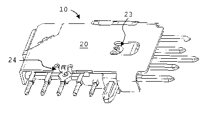
Fig. 10 shows an embodiment of the invention wherein
a signal lead 11 comprises a hole 15, indicated by the dashed
line to contact a further electrical conductor 50 by insertion
a contacting element 51 in said hole 15. Accordingly, an elec-
trical signal can be monitored or tapped from the signal lead
11.
9
CA 02580394 2007-03-14
WO 2006/029668 PCT/EP2005/007491
Figs. 11A - 11E schematically illustrate a cable con-
nector 1 and components thereof as displayed in Fig. 1.
Terminal blocks 61 are stacked and each may comprise a metal-
lic plate 62 having shaped to form a wire management comb as
shown in Fig. 11B. The fingers of the wire management comb can
engage the shielding braids 63 of the twinax wires 64 for
grounding to the ground lead 12. The wire management comb may
be a separate element or part of a shielding plate 20 and may,
for example, be formed along the edge of a shield adjacent the
back end of the terminal block 61
The plates 62 comprise contacting elements 60 with a
deformable structure for engaging a ground lead 12 of an adja-
cent terminal block connector. Again, the contacting elements
may be of the eye of the needle type as shown in Figs. 11B-
11D.
Fig. 11C shows a part of the wire comb in an attached
state. Accordingly, the wires 64 are positioned and the foil
63 is engaged by the press fit connection obtained by holding
the contacting elements 60 in the openings 15 of the ground
lead 12.
Since several terminal blocks 61 are stacked, the
contacting element 60 comprises a bent section 65 provided
with another hole 66, as shown in Fig. 11D. The bent section
65 of the contacting elements 60 allows stacking of the con-
nectors 10 right on top of each other as shown in Fig. 11E.
The stacked terminal blocks 61 are part of the cable connector
1 that further comprises a housing 67 and said contacting ele-
ment 60 contacts said housing. Accordingly, the contacting
element 60 provides improved stacking and electromagnetic
shielding performance.
It should be noted that the embodiment of the connec-
tor described above does not limit the scope of the invention;
further modifications are possible such as other deformable
structures 27 at the distal portion 25 of the connection ele-
ments 23,24. The contacting elements can also be used for
electrically connecting various leads 11,12. Reasons for link-
ing lead include power distribution, in which one lead is
sacrificed in order to take the arc over when plugging the
connector in a powered state or where several beams are used
CA 02580394 2007-03-14
WO 2006/029668 PCT/EP2005/007491
to get an equal spread of the required amount lead material to
handle the power. Another application of linking lead may be
high frequency and differential signal distribution where
leads may be dedicated for the ground return current. In the
case of high frequency applications, the openings in the
shielding plates for providing the contacting elements are
preferably located at the ground leads in order to minimize
openings in the region of the signal leads and therefore
crosstalk.
11