Note: Descriptions are shown in the official language in which they were submitted.
CA 02580562 2007-04-04
DESCRIPTION
POWER STORAGE SYSTEM
TECHNICAL FIELD
[0001]
The present invention relates to a power storage system
that stores DC power for charging/discharging, and the
invention is applicable for example to an electric rolling
stock.
BACKGROUND ART
[0002]
In recent years, it has been known to combine a drive
control inverter provided in an electric rolling stock or a
power supply facility provided in a substation on the ground
or the like with a power storage system to which a power storage
device such as a secondary battery and an electric double-layer
capacitor is applied, so that excess regenerative power
generated by braking a vehicle is stored in the power storage
device and the stored power may efficiently be used for
accelerating the vehicle or addressing drops in the line
voltage, which enables efficient use of the kinetic energy of
the vehicle (see for example Patent Documents 1 and 2).
[0003]
Patent Document 1: JP-A-2003-199354
Patent Document 2: JP-A-2005-206111
DISCLOSURE OF THE INVENTION
1
CA 02580562 2007-04-04
Problems to be Solved by the Invention
[0004]
When a power storage system is put to use, important and
necessary techniques in using the power storage system in a
stable and safe manner concern how to form the elements of the
power storage system including their positional arrangement,
how to operate the elements in connection with one another and
under what condition, how to detect abnormalities in the power
storage system if any, and how to operate the elements in
consideration of the detection result.
However, applications and development of the power
storage system have begun only in recent years, and although
Patent Documents 1 and 2 briefly describe the configuration
and operation of the power storage system, there is no
disclosure about specific methods of operation when the power
storage system is activated, operated, and stopped,
abnormality detecting methods, and methods of operation when
an abnormality is detected.
The present invention was made in view of the
above-described circumstances, and it is an object of the
invention to provide an optimum power storage system for
application to a traction system or the like capable of surely
carrying out activation, operation, and stopping that are
important and necessary in actually using the power storage
system and appropriately addressing various kinds of
2
CA 02580562 2007-04-04
abnormalities.
Means for Solving the Problems
[0005]
An aspect of the present invention is a power storage
system comprising:
a DC-DC converter unit regulating DC power from a DC power
supply into prescribed voltage and current; and
a power storage unit storing DC power'regulated by the
DC-DC converter,
wherein the' power storage system, on the DC power supply
side(the primary side) of the DC-DC converter, includes:
a primary side current detecting unit for
detecting a current of a main circuit;
a primary side voltage detecting unit for
detecting a voltage of the main circuit;
a primary side switch unit for opening and closing
the main circuit; and
a primary side filter unit for reducing harmonics
of the main circuit,
the power storage system, on the power storage unit side
(the secondary side) of the DC-DC converter unit, includes:
a secondary side filter unit for reducing
harmonics of the main circuit;
a secondary side switch unit for opening and
closing the main circuit;
3
CA 02580562 2007-04-04
a secondary side voltage detecting unit for
detecting a voltage of the main circuit; and
a secondary side current detecting unit for
detecting a current of the main circuit, and
the power storage system includes a system control unit
for controlling on/off states of at least the primary side
switch unit, the secondary side switch unit and the DC-DC
converter unit, inputted operational commands from outside of
the power storage system and signals from the primary side
current detecting unit, the primary side voltage detecting unit,
the primary side switch unit, the primary side filter unit,
the DC-DC converter unit, the secondary side filter unit, the
secondary side switch unit, the secondary side voltage
detecting unit, the secondary side current detecting unit and
the power storage unit.
Advantages of the Invention
(0006)
In an aspect of the present invention, an optimum power
storage system for application to a traction system or the like
capable of surely carrying out activation, operation, and
stopping and appropriately addressing various kinds of
abnormalities can be implemented.
BEST MODE FOR CARRYING OUT THE INVENTION
[0007]
First Embodiment
4
CA 02580562 2007-04-04
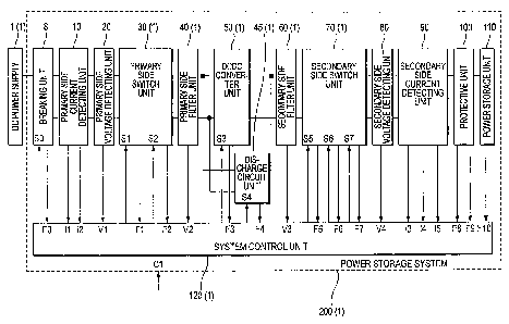
Fig. 1 is a diagram of the configuration of a power storage
system according to a first embodiment of the invention.
As shown in Fig. 1, the power storage system 200(1) is
connected to a DC power supply 1(1), and the power storage
system 200 (1) includes a breaking unit 8 that has current
breaking means, a primary side current detecting unit 10
positioned in the succeeding stage of the breaking unit 8 to
detect current at a primary side main circuit, a primary side
voltage detecting unit 20 positioned in the succeeding state
of the primary side current detecting unit 10 to detect voltage
at the primary side main circuit, a primary side switch unit
30(1) positioned in the succeeding stage of the primary side
voltage detecting unit 20 to open/close the primary side main
circuit, a primary side filter unit 40(1) positioned in the
succeeding stage of the primary side switch unit 30 (1) to reduce
harmonics at the primary side main circuit, a DC-DC converter
unit 50(1) positioned in the succeeding stage of the primary
filter unit 40(1), a secondary side filter unit 60(1)
positioned on the secondary side of the DC-DC converter unit
50(1) to reduce harmonics at a secondary side main circuit,
a discharge circuit unit 45(1) connected to the positive and
negative sides of the primary side filter unit 40(1) and the
positive side of the secondary side filter unit 60(1), a
secondary side switch unit 70(1) positioned in the succeeding
stage of the secondary side filter unit 60(1) to open/close
CA 02580562 2007-04-04
the secondary side main circuit, a secondary side voltage
detecting unit 80 positioned in the succeeding stage of the
secondary side switch unit 70 (1) to detect voltage at the
secondary side main circuit, a secondary side current detecting
unit 90 positioned in the succeeding stage of the secondary
side voltage detecting unit 80 to detect current at the
secondary side main circuit, a protective unit 100 positioned
in the succeeding stage of the secondary side current detecting
unit 90, a power storage unit 110 positioned in the succeeding
stage of the protective unit 100, and a system control unit
120(1) that controls these elements.
[0008J
The system control unit 120 (1) outputs a closing command
SO to the breaking unit 8, closing commands S1 and S2 to the
primary side switch unit 30 (1) , an operation command S3 to the
DC-DC converter unit 50 (1) , a discharge command S4 to the
discharge circuit unit 45(1), and closing commands S5 to S7,
to the secondary side switch unit 70(1).
The system control unit 120(1) is provided with an
auxiliary contact signal FO from the breaking unit 8, primary
side current I1 and primary side differential current 12 from
the primary side current detecting unit 10, primary side
voltage V1 from the primary side voltage detecting unit 20,
auxiliary contact signals Fl and F2 from the primary side switch
unit 30 (1) , primary side capacitor voltage V2 from the primary
6
CA 02580562 2007-04-04
side filter unit 40(1), a status signal F3 from the DC-DC
converter unit 50(1), a status signal F4 from the discharge
circuit unit 45(1), secondary side capacitor voltage V3 from
the secondary side filter unit 60(1), auxiliary contact signals
F5 to F7 from the secondary side switch unit 70 (1) , secondary
side voltage V4 from the secondary side voltage detecting unit
80, secondary side positive current 13, secondary side
differential current 14, and secondary side negative side
current 15 from the secondary side current detecting unit 90,
auxiliary contact signals F8 and F9 from the protective unit
100, and a status signal F10 from the power storage unit 110.
The system control unit 120 (1) is provided with an externally
applied operation command Cl.
The above-described elements are supplied with a control
power supply (not shown) from the side used for example to drive
switches built in the primary side switch unit and the secondary
side switch unit, have the DC-DC converter and the discharge
circuit operated, and have the system control unit and a
computer provided in a converter control unit (that will be
described) operated.
[0009]
Fig. 2 is a diagram of an example of the configuration
of a DC power supply 1(1) according to the first embodiment
of the invention.
As shown in Fig. 2, the DC power supply 1(1) is voltage
7
CA 02580562 2007-04-04
applied between a pantograph lc and a rail li in a circuit
including a DC voltage source la, an overhead contact line 1b,
the pantograph lc, and the rail li.
[0010]
Fig. 3 is a diagram of an example of the configuration
of the breaking unit 8 according to the first embodiment of
the invention.
As shown in Fig. 3, the breaking unit 8 includes a switch
8a.
The switch 8a is a switch (so-called breaker) capable
of automatically breaking a circuit without an externally
applied command if excess current is passed.
[0011]
Fig. 4 is a diagram of an example of the configuration
of the primary side current detecting unit 10 according to the
first embodiment of the invention.
The unit includes a current detector 11 that detects the
primary side current I1 and a current detector 12 that detects
the differential current 12 between the positive side and the
negative side.
The current detectors both detect current by converting
a flux generated by the current passing across each current
detector into a current value, while they may have other
structures.
The positive side line and the negative side line are
8
CA 02580562 2007-04-04
penetrated through the current detector 12 in the manner in
which their current directions are opposite to each other.
When the circuit operates normally, the positive side current
and the negative side current have equal magnitudes and
directed in different directions, and therefore the sum of the
fluxes generated by the positive current and the negative side
current is zero, so that the current value detected by the
current detector 12 is zero. However, once leakage current
is generated because of degraded line insulation or the like,
the current partly passes across a part other than the line
such as the metal case of the device, which causes the positive
side current and the negative side current to be different from
each other in magnitude, the sum of the fluxes generated by
the positive current and the negative side current penetrating
through the current detector 12 is no longer zero, so that the
output 12 of the current detector 12 is not zero.
The system control unit 120 (1) can monitor the primary
side differential current 12 to detect the leakage current.
The current leakage is caused by degraded line insulation
or the like, which could give rise to a short circuit or a ground
fault unless quick recovery is made. Current leakage is
detected when it is still in a small amount and input to the
system control unit 120 (1) and appropriate measures that will
be described are taken, so that a short circuit or a ground
fault can be prevented.
9
CA 02580562 2007-04-04
The primary side current I1 and the secondary side
differential current 12 detected by the current detectors 11
and 12 are output to the system control unit 120(1).
Note that the primary side current detecting unit 10 may
be provided immediately after the breaking unit 8 (preceding
the primary side voltage detecting unit 20), so that the
differential current can be detected upstream of the circuit
in view of the DC power supply 1(1) , and the range of the circuit
that can be detected for leakage current caused by voltage from
the DC power supply 1(1) can be maximized.
[0012]
Fig. 5 is a diagram of an example of the configuration
of the primary side voltage detecting unit 20 according to the
first embodiment of the invention.
As shown in Fig. 5, the primary side voltage detecting
unit 20 includes a voltage detector 21 that detects the voltage
between the positive side and the negative side. The detected
primary side voltage V1 is output to the system control unit
120(l).
[0013]
Fig. 6 is a diagram of an example of the configuration
of the primary side switch unit 30 (1) according to the first
embodiment of the invention.
As shown in Fig. 6, the primary side switch unit 30(1)
includes a switch 31a arranged in series with the positive side
CA 02580562 2007-04-04
and a series circuit having a switch 31b and a charging resistor
32 arranged in parallel to the switch 31a. The switches 31a
and 31b are provided with closing signals S1 and S2,
respectively and auxiliary contact signals Fl and F2 (that will
be described) are input from the switches 31a and 31b to the
system control unit 120(1).
[0014]
Fig. 7 is a diagram of an example of the configuration
of the switches 8a, 31a, 31b, and 71a to 71c according to the
first embodiment of the invention. Note that the switches 71a
to 71c will be described later.
As shown in Fig. 7, the configuration includes a main
contact 31althat opens/closes the main circuit, a closing coil
31a3 that drives the main contact 31a1, and auxiliary contacts
31a2 mechanically connected to the main contact 31a1 to be
closed/opened in response to the closing/opening of the main
contact 31a1.
The closing coil 31a3 is a electromagnetic coil that is
turned on/off in response to closing commands SO to S2 and S5
to S7 input from the system control unit 120 (1) , and the main
contact 31a1 is closed/opened in response to the
presence/absence of the driving force of the coil.
The auxiliary contact signals FO to F2 and F5 to F7
indicating the operation of the main contact 31a1 detected by
the auxiliary contact 31a2 are output to the system control
11
CA 02580562 2007-04-04
unit 120(1).
Note that in the above description, the switches 8a, 31a,
31b, and 71a to 71c are mechanical switches, but the switches
may be other kinds of switches such as semiconductor type
contactless switches as long as the opening and closing and
the operation confirmation of the circuit can be carried out
using them.
The auxiliary contact 31a2 is closed in response to the
closing of the main contact 31a1 and opened in response to its
opening. Conversely, the auxiliary contact may be
opened/closed in response to the closing/opening of the main
contact 31a1.
In this way, a signal from an auxiliary contact linked
with the main contact is input to the system control unit 120 (1),
and the operation of the switch can surely be recognized by
the system control unit, so that activation, operation, and
stopping steps can be ensured, and abnormalities in the
switches can be detected.
[0015]
Fig. 8 is a diagram of an example of the configuration
of the primary side filter unit 40(1) according to the first
embodiment of the invention.
As shown in Fig. 8, a voltage detector 42 is connected
in the succeeding stage of a reactor 41. Primary side capacitor
voltage V2 detected by the voltage detector 42 is output to
12
CA 02580562 2007-04-04
the system control unit 120(1).
A noise filter 44 is connected in the succeeding stage
of the voltage detector 42, and a primary side capacitor 43
is connected in the succeeding stage of the noise filter 44.
[0016]
The noise filter 44 generates impedance for noise
components (common mode noise) flowing the positive side line
and the negative side line in the same direction in order to
reduce the noise from flowing to the outside and the filter
can be implemented by arranging a ring-shaped core member made
of a material such as ferrite and amorphous through the positive
and negative side lines while the center of the core member
is directed so that the current directions of these lines are
opposite to each other.
In order to increase the impedance, the core member may
be turned multiple times in the positive and negative side lines
in the same direction.
The noise filter 44 is preferably provided preceding and
near the primary side capacitor 43.
With the noise filter 44 provided in this way, a power
storage system with less external noise flow can be provided.
[0017]
A circuit (not shown) having two capacitors with a good
high frequency characteristic connected in series may be
connected to the primary side capacitor 43 in parallel, and
13
CA 02580562 2007-04-04
the mid point in the series-connection may be grounded to the
case, so that common mode noise flow can be reduced. If the
arrangement is used together with the noise filter 44, the
common mode noise can be reduced even more effectively.
[0018]
Note that when the voltage detector 42 is connected in
the succeeding stage of the noise filter 44, the noise filter
44 may function as impedance to common mode noise current
generated by the DC-DC converter unit 50(1) (that will be
described) connected in parallel in the succeeding stage of
the primary side capacitor 43, and therefore the common mode
noise current flows into the system control unit 120 (1) through
the voltage detector 42 whose impedance is relatively reduced,
which could give rise to errors in the operation of the system
control unit 120(1). The voltage detector 42 connected in the
preceding stage of the noise filter 44 allows the common mode
noise current generated from the DC-DC converter 50 (1) to flow
into the system control unit 120(1) through the voltage
detector 42 and erroneous operation can be prevented.
[0019]
Fig. 9 is a diagram of an example of the configuration
of the DC-DC converter unit 50(1) according to the first
embodiment of the invention.
As shown in Fig. 9, the DC-DC converter unit 50(1)
includes a converter circuit 51a and a converter control unit
14
CA 02580562 2007-04-04
52a, an operation command S3 is input from the system control
unit 120(1) to the converter control unit 51a, and a status
signal F3 is output from the converter control unit 52a to the
system control unit 120(1).
[0020]
Fig. 10 is a diagram of an example of the configuration
of the converter circuit 51a.
As shown in Fig. 10, the circuit includes a bidirectional
buck-boost converter circuit including four switching
elements 51a1 to 51a4 and a coupling reactor 51a5. The circuit
is capable of controlling power flow in the two directions
regardless of which is greater between the primary side voltage
(at the left side terminal in the figure) and the secondary
side voltage (at the right side terminal in the figure) in the
converter circuit.
In this way, voltage at the power storage unit 110 can
be set to a higher level than the voltage of the DC power supply
la, and current in the circuits in and after the DC-DC converter
unit 50(1) can be reduced accordingly, which allows the
components to be reduced in size, so that a compact and
lightweight power storage system can be obtained.
[0021]
As shown in Figs. 9 and 10, the converter control unit
52a is provided with an operation command S3 from the system
control unit 120(1) and the command includes the operation,
CA 02580562 2007-04-04
stopping, or control mode of the DC-DC converter, and command
values (target values) for power to be passed between the
primary side and the secondary side, coupling reactor current
ILP (or ILN), converter primary side current I1P (or I1N),
converter secondary side current 12P (or 12N), primary side
capacitor voltage V2, and secondary side capacitor voltage V3.
The status signal F3 of the DC-DC converter 50 (1) is input from
the converter control unit 52a to the system control unit
120(1).
The status signal F3 includes the voltage, current, and
temperature of the elements, the on/off states and the failure
state of the switching elements in the DC-DC converter 50 (1) .
The converter control unit 52a carries out PWM control to the
switching elements 51a1 to 51a4 of the converter circuit 51a
in response to the operation command S3.
[0022]
Fig. 11 is a diagram of an example of the configuration
of a discharge circuit unit 45(1) according to the first
embodiment of the invention.
As shown in Fig. 11, a primary side diode 46a is connected
to a line led from the positive side of the succeeding stage
of the primary side filter unit 40(1), and a secondary side
diode 46b is connected to a line led from the positive side
of the preceding stage of the secondary side filter unit 60 (1) .
The cathode sides of the diodes are butted against each other
16
CA 02580562 2007-04-04
and the positive side of a circuit having a discharge element
46c and a discharging resistor 46e connected in series is
connected to the butt point, while its negative side is
connected to the negative side line.
The on/off state of the discharge element 46c is
controlled by a discharge element driving circuit 46d. The
discharge element driving circuit 46d is provided with a
discharge command S4 including an on/off command for the
discharge element 46c from the system control unit 120 (1), and
a status signal F4 including the operation state of the
discharge element 46c is input from the discharge element
driving circuit 46d to the system control unit 120(1).
In this way, the primary side diode 46a and the secondary
side diode 46b are butted against each other, so that the
primary and secondary side capacitors 43 and 63 can be
discharged by the one discharge element 46c, so that a compact
and lightweight discharge circuit unit can be provided.
[0023]
Fig. 12 is a diagram of an example of the configuration
of the secondary filter unit 60(1) according to the first
embodiment of the invention.
As shown in Fig. 12, a noise filter 64 is connected in
the succeeding stage of the secondary side capacitor 63, and
a voltage detector 62 that detects the secondary side capacitor
voltage V3 is provided in the succeeding stage. The signal
17
CA 02580562 2007-04-04
V3 detected by the voltage detector 62 is output to the system
control unit 120. A reactor 61 is connected in the succeeding
stage of the voltage detector 62.
[0024]
The configuration of the noise filter 64 is the same as
that of the noise filter 44 and therefore the description will
not be provided.
The noise filter 64 is preferably provided succeeding
and near the secondary side capacitor 63.
A circuit (not shown) having two capacitors with a good
high frequency characteristic connected in series may be
connected to the secondary side capacitor 63, and the mid point
in the series-connection may be grounded to the case, so that
common mode noise flow can be reduced. If the arrangement is
used together with the noise filter 64, the common mode noise
can be reduced even more effectively.
[0025]
The reactor 61 is provided to reduce ripple current
generated at the DC-DC converter unit 50(1).
Note that if the voltage detector 62 is connected in the
preceding stage of the noise filter 64, the noise filter 64
serves as impedance to common mode noise current generated from
the DC-DC converter unit 50(1) connected in parallel to the
capacitor 63, so that the common mode noise current is allowed
to flow into the system control unit 120 (1) through the voltage
18
CA 02580562 2007-04-04
detector 62 whose impedance is relatively reduced, which could
give rise to errors in the operation of the system control unit
120(1). The voltage detector 62 connected in the succeeding
stage of the noise filter 64 allows the common mode noise
current generated from the DC-DC converter 50 (1) to flow into
the system control unit 120(1) through the voltage detector
62 and erroneous operation can be prevented.
[00261
Fig. 13 is a diagram of an example of the configuration
of the secondary side switch unit 70 (1) according to the first
embodiment of the invention.
As shown in Fig. 13, the primary side switch unit 70 (1)
includes a switch 71a arranged in series with the positive side,
a series-circuit having a switch 71b and a charging resistor
72 connected in parallel thereto, and a switch 71c arranged
in series with the negative side.
Switches 71a to 71c are provided with closing signals
S5 to S7 from the system control unit 120(1), and auxiliary
contact signals F5 to F7 indicating the operation of the
switches 71a to 71c are input from these switches to the system
control unit 120(1).
The internal configuration of the switches 71a to 71c
are the same as that shown in Fig. 7 and therefore the
description will not be provided.
Note that the described switches 71a to 71c are
19
CA 02580562 2007-04-04
mechanical switches, but the switches may be other kinds of
switches such as semiconductor type contactless switches as
long as the opening and closing and the operation confirmation
of the circuit can be carried out using them.
[0027]
Fig. 14 is a diagram of an example of the configuration
of the secondary side voltage detecting unit 80 according to
the first embodiment of the invention.
As shown in Fig. 14, the secondary side voltage detecting
unit 80 is made of a voltage detector 81 that detects secondary
side voltage V4. The detected signal V4 is output to the system
control unit 120(1).
[0028]
Fig. 15 is a diagram of an example of the configuration
of the secondary side current detecting unit 90 according to
the first embodiment of the invention.
As shown in Fig. 15, the unit includes a current detector
91 that detects positive side secondary current 13, a current
detector 92 that detects the differential current 14 between
the positive side and the negative side, and a current detector
93 that detects negative side secondary side current 15.
These current detectors each operate by converting a flux
generated by current passing through each current detector into
a current value.
The current detector 92 is used to detect leakage current
CA 02580562 2007-04-04
caused by circuit insulation degradation, details of which are
the same as those of the current detector 12 and therefore the
description will not be provided.
Note that the secondary side current detecting unit 90
may be provided immediately before the protective unit 100
(succeeding the secondary side voltage detecting unit 80), so
that differential current in the immediate vicinity of the
power storage unit 110 can be detected. Therefore, the
differential current can be detected upstream of the circuit
in view of the power storage unit 110, and the range of the
circuit that can be detected for leakage current caused by
voltage from the power storage unit 110 can be maximized.
[0029]
The secondary side positive side current 13, the
secondary side differential current 14, and the secondary side
negative side current 15 detected by the current detectors 91
to 93 are output to the system control unit 120(1).
Note that without providing the current detector 92, only
the signals 13 and 15 from the current detectors 91 and 92 may
be input to the system control unit 120 (1) , where the difference
between the signals may be operated for evaluation, and still
the same advantages result.
[0030]
Fig. 16 is a diagram of an example of the configuration
of the protective unit 100 according to the first embodiment
21
CA 02580562 2007-04-04
of the invention.
As shown in Fig. 16, the unit includes a positive side
fuse 101a and a negative side fuse lOib, and opens the circuit
by blowing in response to passage of excess current
therethrough. The fuses have auxiliary contacts 102a and 102b
for detecting fuse blowing as the contacts are closed by
blowing.
Auxiliary contact signals F8 and F9 indicating the states
of the auxiliary contacts 102a and 102b are output to the system
control unit 120(1).
Note that the blowing may be detected when the fuses lOla
and 101b are blown to open the contacts, and the auxiliary
contacts may be detecting circuits made of an electronic
circuit rather than the mechanical contacts.
A switch (so-called breaker) capable of automatically
breaking the circuit in response to excess current without an
externally applied command may be employed instead of the
fuses.
With the fuse being provided on the negative side in
addition to the one on the positive side, the circuit can be
interrupted if the negative side line preceding the fuse lOlb
and the contacts of cells 111 in the power storage unit 110
short circuit, so that a power storage system with a higher
protective function can be obtained.
[0031]
22
CA 02580562 2007-04-04
Fig. 17 is a diagram of an example of the configuration
of the power storage unit 110 according to the first embodiment
of the invention.
As shown in Fig. 17, a plurality of cells 111 each made
of an electric double-layer capacitor or a secondary battery
are provided in a series-parallel arrangement, so that
necessary voltage and capacitance can be provided between the
terminals of the power storage unit.
Various kinds of information such as the voltage, the
current, the amount of stored power, the temperature, and the
pressure of the cells 111 or the elements of the power storage
unit 110 are collected by a power storage unit monitor 112 and
output to the system control unit 120(1) as a status signal
F10.
[0032]
The operation steps from the activation through the
steady state operation to the stopping of the power storage
system 200(1) according to the first embodiment will be
described.
Note that there may be two methods of activating the power
storage system, one is to charge the primary side capacitor
43 or the secondary side capacitor 63 from the DC power supply
la to activate and operate the system (which will hereinafter
be referred to as "primary side activation"), and the other
is to charge the primary side capacitor 43 or the secondary
23
CA 02580562 2007-04-04
side capacitor 63 using energy stored in the power storage unit
110 to activate and operate the system (which will hereinafter
be referred to as "secondary side activation").
Now, the operation steps in the primary side activation
will be described first and then the operation steps in the
secondary side activation will be described.
[0033]
Primary Side Activation
[0034]
Step lA-1
If the control power supply for the system control unit
120 (1) is turned on, and an operation command Cl including an
activation command is input from the outside, a closing command
SO for the switch 8a is output, the coil 31a3 of the switch
8a is excited, and the main contact 31a1 is closed accordingly.
If the state in which the closing command SO is on, the
auxiliary contact 31a2 of the switch 8a is surely closed and
the auxiliary contact signal FO is on continues for a certain
period, the system control unit 120(1) recognizes that the
switch 8a has normally been turned on.
[0035]
Step 2A-1
If the state in which the primary side voltage V1 detected
by the voltage detector 21 is at a prescribed value or more
continues for a certain period after the system control unit
24
CA 02580562 2007-04-04
120 (1) determines the normal turning on of the switch 8a, the
system control unit outputs a closing command S2, so that the
coil 31a3 of the switch 31b is excited and the main contact
31a1 is closed accordingly. In this way, the primary side
capacitor 43 is charged through the charging resistor 32.
The system control unit 120(1) determines the normal
turning on of the switch 31b if the state in which the closing
command S2 is on, the auxiliary contact 31a2 of the switch 31b
is surely closed, and the auxiliary contact signal F2 is on
continues for a certain period. Then, after a prescribed
period or if the difference between the primary side voltage
V1 and the secondary side capacitor voltage V2 is equal to or
lower than a prescribed value and then a prescribed period
elapses, the system control unit determines that the charging
of the primary side capacitor 43 is complete, and outputs a
closing command S1. In this way, the coil 31a3 of the switch
31a is excited and the main contact 31a1 is closed accordingly.
The system control unit120(1) recognizes that the switch
31a has normally been turned on if the state in which the
auxiliary contact 21a2 of the switch 31a is surely closed and
the auxiliary contact signal Fl is on continues for a certain
period.
[0036]
Step 3A-1
Upon recognizing the normal closing of the switch 31a,
CA 02580562 2007-04-04
the system control unit 120(1) outputs an operation command
S3 to the converter control unit 52a. At the time, the command
S3 includes an command to have the DC-DC converter 50(1)
operated in an initial charging mode in order to charge the
secondary side capacitor 63, the secondary side capacitor
voltage V3, and the secondary side voltage V4. Upon receiving
the operation command S3, the converter control unit 52a
controls the converter circuit 51a so that the secondary side
capacitor voltage V3 equals the secondary side voltage V4, and
necessary power is passed from the primary side to the secondary
side of the converter to charge the secondary side capacitor
63.
Note that in order to prevent the secondary side
capacitor 63 or the like from being damaged by abrupt charging,
the secondary side capacitor 63 is charged while the converter
control unit 52a controls the current in the converter circuit
51a so that the current passed from the primary side to the
secondary side is restricted to a prescribed value.
The system control unit 120(1) determines that the
charging of the secondary side capacitor 63 is complete if the
difference between the secondary side capacitor voltage V3 and
the secondary side voltage V4 is equal to or lower than the
prescribed value, and then a prescribed period has been
elapsed.
[0037]
26
CA 02580562 2007-04-04
Step 4A-1
Upon determining that the charging of the secondary side
capacitor 63 is complete, the system control unit 120 (1) turns
on closing commands S5 and S7 that turn on the switches 71a
and 71c. This drives the power coils 31a3 of the switches 71a
and 71c, and the main contact 31a1 is closed accordingly. In
this way, the auxiliary contact 31a2 liked to the main contact
31a1 is closed, and auxiliary contact signals F5 and F7
indicating the state of the auxiliary contacts 31a2 are output
to the system control unit 120(1).
The system control unit 120(1) recognizes that the
turning on of the switches 71a and 71c is complete if the state
in which the closing commands S5 and S7 are on, the auxiliary
contacts 31a2 of the switches 71a and 71c are surely closed
and the auxiliary contact signals F5 and F7 are on continues
for a certain period.
Note that the switches 71a and 71c may be turned on either
simultaneously or sequentially. When they are sequentially
turned on, the peak power necessary for turning them on may
be reduced, and only the switch to be turned on last may serve
as a switch capable of opening and closing current. A switch
capable of opening and closing current is generally large in
size, while the number of such switches may be reduced and
therefore a compact and lightweight power storage system can
be obtained.
27
CA 02580562 2007-04-04
[0038]
Step 5A-1
Upon determining that the switches 71a and 71c has
normally been turned on, the system control unit 120 (1) outputs
an operation command S3 to have the converter control unit 52a
operated while keeping the current ILP (or the negative side
current ILN) of the coupling reactor 51a5 at zero.
In this way, the converter control unit 52a controls the
converter circuit 51a so that the current IL (or the negative
side current ILN) of the coupling reactor 51a5 is at zero.
Note that the converter primary side current I1P (or I1N)
may be controlled to be zero, the converter secondary side
current 12P (or 12N) may be controlled to be zero, or the primary
side current 11 detected by the current detector 11 or the
secondary side positive side current 13 detected by the current
detector 91 may be controlled to be zero. The secondary side
negative side current 15 as the detection value of the current
detector 93 may be zero instead of the current detector 91.
The system control unit 120(1) determines that the
converter control unit 52a is normal if the state in which the
detection value of the current to be controlled is a prescribed
value or less continues for a certain period.
[0039]
Step 6A-1
After determining that the converter control unit 52a
28
CA 02580562 2007-04-04
is normal, the system control unit 120 (1) inputs an operation
command S3 including a current command I* or a power command
P* to the converter control unit 52a.
In this way, the converter control unit 52a controls so
that its current or the power between the primary side and the
secondary side matches the command.
Note that the current to be controlled is one of the
current ILP (or the negative side current ILN) of the coupling
reactor 51a5, the converter primary side current I1P (or the
negative side current I1N), and the converter secondary side
current 12P (or 12N).
An operation command S3 including a voltage command V*
may be input to the converter control unit 52a from the system
control unit 120(1), and in this case the converter control
unit 52a controls the converter circuit 51a so that a designated
one of the primary side capacitor voltage V2 and the secondary
side capacitor voltage V3 matches the voltage command V*.
[0040]
Step 7A-1
Upon receiving an externally input operation command Cl
including a stopping command, the system control unit 120(1)
inputs an operation command S3 to the converter control unit
52a to gradually reduce the converter current to zero.
The converter control unit 52a controls the converter
circuit 51a to gradually reduce the current, eventually to
29
CA 02580562 2007-04-04
zero.
The time required for reducing the current to zero can
arbitrarily be set.
If the state in which the current is at a prescribed value
or less continues for a certain period, the system control unit
120(1) inputs an operation command S3 to stop the DC-DC
converter 50 (1) , and the converter control unit 52a turns off
the switching elements 51a1 to 51a4 and outputs the state as
a status signal F3.
The system control unit 120(1) determines that the DC-DC
converter 50 (1) has normally been stopped based on the status
signal F3.
Note that the current to be controlled is one of the
current ILP (or ILN) of the coupling reactor 51a5, the converter
primary side current I1P (or the negative side current I1N),
and the converter secondary side current 12P (or I2N).
In this way, the current is reduced to zero and then the
switching elements 51a1 to 52a4 are turned off, so that the
primary side capacitor voltage V2 or the secondary side
capacitor voltage V3 can be prevented from abruptly changing
and excess voltage or the like can be prevented.
[0041]
Step 8A-1
Upon confirming that the DC-DC converter 50(1) has
normally been stopped, the system control unit 120(1) turns
CA 02580562 2007-04-04
M =
off the closing commands SO, S1, S2, and S5 to S7 in order to
open the switches 8a, 31a, 31b, and 71a to 71c.
The system control unit 120(1) confirms auxiliary
contact signals FO to F2 and F5 to F7 indicating the states
of the auxiliary contacts 31a2 in the switches 8a, 31a, 31b,
and 71a to 71c, and determines that the switches 8a, 31a, 31b,
and 71a to 71c have normally been opened upon confirming that
the switches are off.
In this way, the switches 8a, 31a, 31b, and 71a to 71c
are opened based on the confirmation of the stopped state of
the DC-DC converter 50 (1) , so that the switches 8a, 31a, 31b,
and 71a to 71c can be opened with no current application, which
prevents electrical wear of the main contacts in the switches
8a, 31a, 31b, and 71a to 71c.
[0042]
Secondary Side Activation
[0043]
Step 1B-1
If the control power supply for the system control unit
120(1) is turned on and an externally applied command Cl
including an activation command is input, the system control
unit 120 (1) confirms a status signal F10 from the power storage
unit monitor 112 in the power storage unit 110 and turns on
closing commands S6 and S7 for the switches 71b and 71c provided
that there is no abnormality and the state in which the
31
CA 02580562 2007-04-04
secondary side voltage V4 detected by the voltage detector 81
is at a prescribed value or more continues for a certain period.
In this way, the closing coils 31a3 of the switches 71b and
71c are driven, and the main contacts 31a1 are closed. This
causes the auxiliary contacts 31a2 linked with the main
contacts 31a1 to be closed, and auxiliary contact signals F6
and F7 indicating the states of the auxiliary contacts 31a2
are output to the system control unit 120(1).
The system control unit 120(1) recognizes the normal
turning on of the switches 71b and 71c if the state in which
the closing commands S6 and S7 are on, the auxiliary contacts
31a2 of the switches 71b and 71c are surely closed and the
auxiliary contact signals F6 and F7 are on continues for a
certain period.
Note that the switches 71b and 71c may be turned on either
simultaneously or sequentially. When they are sequentially
turned on, the peak power necessary for turning them on can
be reduced, and therefore a control power supply with only a
small peak withstand voltage may be employed, so that a compact
and lightweight power storage system can be obtained.
The switches 71b and 71c are turned on, so that the
secondary side capacitor 63 is charged through the charging
resistor 72.
The system control unit 120(1) recognizes that the
switches 71b and 71c have normally been turned on, then
32
CA 02580562 2007-04-04
determines that the secondary side capacitor 63 has been
charged and outputs an closing command S5 if the state continues
for a certain period or if the difference between the secondary
side voltage V4 and the secondary side capacitor V3 is a
prescribed value or less and then a prescribed period elapses.
In this way, the coil 31a3 of the switch 71a is excited and
the main contact 31a1 is closed accordingly.
The system control unit 120(1) recognizes that the switch
71a has normally been turned on if the state in which the
auxiliary contact 31a2 of the switch 71a is surely closed and
the auxiliary contact signal F5 is on continues for a certain
period.
[0044]
Step 2B-1
Upon confirming that the switch 71a has normally been
turned on, the system control unit 120 (1) outputs an operation
command S3 to the converter control unit 52a. At the time,
the command S3 includes a command to have the DC-DC converter
50 (1) operated in an initial charging mode in order to charge
the primary side capacitor 43, the primary side capacitor
voltage V2, and the primary side voltage V1. Upon receiving
the operation command S3, the converter control unit 52a has
the converter circuit 51a operated so that necessary power is
passed from the secondary side to the primary side and the
primary side capacitor 43 is charged.
33
CA 02580562 2007-04-04
Note that in order to prevent the primary side capacitor
43 or the like from being damaged by abrupt charging, the
primary side capacitor 43 is charged while the converter
control unit 52a controls current in the converter circuit 51a
so that the current passed from the secondary side to the
primary side is restricted to a prescribed value.
The converter control unit 52a controls the converter
circuit 51a so that the primary side capacitor voltage V2 is
equal to the primary side voltage Vl or the primary side
capacitor voltage V2 is equal to a predetermined value.
The system control unit 120(1) determines the charging
of the primary side capacitor 43 is complete if the difference
between the primary side capacitor voltage V2 and the primary
side voltage V1 is a prescribed value or less and then a
prescribed period elapses or if the primary side capacitor
voltage V2 reaches the predetermined prescribed value.
[0045]
Step 3B-1
Upon determining that the charging of the primary side
capacitor 43 is complete, the system control unit 120 (1) turns
on the closing command Si to turn on the switch 31a. This drives
the closing coil 31a3 of the switch 31a and the main contact
31a1 is closed. Then, the auxiliary contact 31a2 linked with
the main contact 31a1 is closed, so that the auxiliary contact
signal Fl indicating the state of the auxiliary contact 31a2
34
CA 02580562 2007-04-04
is output to the system control unit 120(1).
The system control unit 120(1) recognizes the normal
turning on of the switch 31a if the state in which the closing
command Sl is on, the auxiliary contact 31a2 of the switch 31a
is surely closed and the auxiliary contact signal Fl is on
continues for a certain period.
Step 4B-1
The system control unit 120(1) recognizes the normal
turning on of the switch 31a, then outputs a closing command
SO for the switch 8a, excites the coil 31a3 of the switch 8a,
and closes the main contact 31a1. The system control unit
120(1) recognizes the normal turning on of the switch 8a if
the state in which the closing command SO is on and the auxiliary
contact 31a2 of the switch 8a is surely closed to turn on the
auxiliary contact signal FO continues for a certain period.
[0046]
Step 5B-1
Upon determining that the switch 8a has normally been
turned on, the system control unit 120 (1) outputs an operation
command S3 to have the converter control unit 52a operated so
that the current ILP (or the negative side current ILN) of the
coupling reactor 51a5 is at zero.
In this way, the converter control unit 52a has the
converter circuit 51a operated so that the current ILP (or the
negative side current ILN) of the coupling reactor 51a5 is at
CA 02580562 2007-04-04
zero.
Note that the control can be carried out so that the
converter primary side current IiP (or I1N) becomes zero, the
converter secondary side current 12P (or 12N) becomes zero,
or the primary side current I1 detected by the current detector
11 or the secondary side positive side current 13 detected by
the current detector 91 becomes zero.
Note that the secondary side negative side current 15
as the detection value of the current detector 93 may become
zero instead of the secondary side positive side current 13.
The system control unit 120(1) determines that the
converter control unit 52a is normal if the state in which the
detection value for the current to be controlled is a prescribed
value or less for a prescribed period.
[0047]
Step 6B-i
Upon determining that the converter control unit 52a is
normal, the system control unit 120(1) inputs an operation
command S3 including a current command I* or a power command
P* to the converter control unit 52a.
In this way, the converter control unit 52a controls its
current or the power between the primary side and the secondary
side to mach the command.
Note that the current to be controlled is one of the
current ILP (or the negative side current ILN) of the coupling
36
CA 02580562 2007-04-04
reactor 51a5, the converter primary side current I1P (or I1N) ,
and the converter secondary current 12P (or 12N).
An operation command S3 including a voltage command V*
may be input to the converter control unit 52a from the system
control unit 120(1), and the converter control unit 52a
controls the converter circuit 51a so that a designated one
of the primary side capacitor voltage V2 and the secondary side
capacitor voltage'V3 matches the voltage command V*.
[0048)
Step 7B-1
The system control unit 120(1) inputs an operation
command S3 to the converter control unit 52a so that the
converter current is gradually reduced to zero if an externally
applied operation command Cl including a stopping command is
input.
The converter control unit 52a controls the converter
circuit 51a to gradually reduce the current, eventually to zero.
The time necessary for reducing the current to zero can
arbitrarily be set. If the state in which the current is at
a prescribed value or less continues for a certain period, the
system control unit 120(1) inputs an operation command S3 to
stop the DC-DC converter 50 (1) , and the converter control unit
52a turns off the switching elements 51a1 to 51a4 and outputs
the state as a status signal F3. The system control unit 120 (1)
confirms that the DC-DC converter 50(1) has normally been
37
CA 02580562 2007-04-04
stopped based on the status signal F3.
Note that the current to be controlled is one of the
current ILP (or the negative side current ILN) of the coupling
reactor 51a5, the converter primary side current I1P (or 11N) ,
and the converter secondary side current I2P (or 12N).
In this way, the current is reduced to zero and then the
switching elements 51a1 to 51a4 are turned off, so that the
primary side capacitor 'voltage V2 or the secondary side
capacitor voltage V3 can be prevented from abruptly changing
and excess voltage or the like can be prevented.
[0049]
Step 8B-1
Upon determining that the DC-DC converter 50(1) has
normally been stopped, the system control unit 120(1) turns
off the closing commands SO to S2 and S5 to S7 to have the
switches 8a, 31a, 31b, and 71a to 71c opened.
Upon confirming that the switches 8a, 31a, 31b, and 71a
to 71c are surely off based on the auxiliary contact signals
FO to F2 and F5 to F7 that indicate the states of the auxiliary
contacts 31a2 of these switches, the system control unit 120(1)
determines that the switches 8a, 31a, 31b, and 71a to 71c have
normally been opened.
In this way, the switches 8a, 31a, 31b, and 71a to 71c
are opened after it is confirmed that the DC-DC converter 50 (1)
is stopped, so that the switches 8a, 31a, 31b, and 71a to 71c
38
CA 02580562 2007-04-04
can be opened with no current application, and therefore
electrical wear of the main contacts of these switches 8a, 31a,
31b, and 71a to 71c can be prevented.
[0050]
By the operation steps described above from the
activation through the steady state operation to the stopping,
a power storage system capable of reliable operation can be
obtained.
Note that if only the operation by the primary side
activation is necessary, the switch 71b of the secondary side
switch unit 70 (1) and the charging resistor 72 are not necessary
and may be removed.
Meanwhile, if only the operation by the secondary side
activation is necessary, the switch 31b of the secondary side
switch unit 30 (1) and the charging resistor 32 are not necessary
and may be removed.
[0051]
Now, a method of detecting abnormalities and operation
to be carried out upon detecting an abnormality in the power
storage system according to the first embodiment will be
described in detail.
In order to allow the power storage system to operate
in a safe and stable manner, appropriate measures must be taken
quickly in response to the kind of an abnormality in each
element of the power storage system. Therefore, a method of
39
CA 02580562 2007-04-04
detecting abnormalities and measures to address the kinds of
the abnormalities that are crucial will be described.
[0052)
Abnormality Detection 1-1
Differential Current Abnormality Detection
If the state in which the primary side differential
current 12 or the secondary side differential current 14 as
the output of the current detector 12 'or 92 is more than a
prescribed value continues for a certain period, the system
control unit 120(1) determines that there is increase in
leakage current caused by insulation degradation somewhere in
the circuit, turns off the closing signals SO to S2 and S5 to
S7 for the switches 8a, 31a, 31b, and 71a to 71c, turns off
the switching elements 51a1 to 51a4 of the DC-DC converter 50 (1),
and inputs a discharge command S4 to the discharge circuit unit
45 (1) so that the primary side capacitor 43 and the secondary
side capacitor 63 are discharged.
The above-described operation allows the increase in
leakage current to be detected and the power storage system
to be quickly stopped, so that further damages can be prevented.
Note that such prescribed values may be provided in a
plurality of stages, and if the differential current is
sufficiently insignificant, the value may be recorded by a
storage device (not shown) or indicated by an indicator lamp
(not shown) in the system control unit, the device, the driver's
CA 02580562 2007-04-04
seat or the like for encouraging checking without stopping the
power storage system.
[0053]
Abnormality Detection 2-1
Switch Abnormality Detection
The system control unit 120 (1) determines that the switch
8a has an abnormality if the state continues for a certain
period in which the main contact 31a1 is not closecl for a failure
in the closing coil 31a3 of the switch 8a or the like though
the closing command SO for the switch 8a is on, the auxiliary
contact 31a2 is not closed accordingly, and the auxiliary
contact signal FO is not turned on or if the state continues
for a certain period in which the closing command SO is off
while the auxiliary contact 31a2 is on and the auxiliary contact
signal FO is on.
Note that abnormalities are detected for the switches
31a, 31b, and 71a to 71c by the same method. If an abnormality
is detected in any of the switches 8a, 31a, 31b, and 71a to
71c, the system control unit 120(1) turns off the closing
commands SO to S2 and S5 to S7 for all the switches 8a, 31a,
31b, and 71a to 71c, turns off the switching elements 51a1 to
51a4 of the DC-DC converter 50(l), and inputs a discharge
command S4 to the discharge circuit unit 45(1), so that the
primary side capacitor 43 and the secondary side capacitor 63
are discharged.
41
CA 02580562 2007-04-04
In this way, a failure in the switch is detected and the
power storage system can quickly be stopped, so that further
damages can be prevented.
[0054]
Abnormality Detection 3-1
Primary Side Capacitor Charging Abnormality Detection (in
Primary Side Activation)
Upon determining that the switch 31b has normally been
turned on in the above-described step 2A-1 in the primary side
activation, the system control unit 120(1) determines that
charging cannot be completed because of an abnormality such
as a ground fault in the primary side capacitor 43 if the
difference between the primary side voltage V1 and the primary
side capacitor voltage V2 is a prescribed value or higher after
a prescribed period or if the primary side current Il is passed
in an amount equal to or higher than a prescribed value. Then,
the system turns off the closing command SO to S2 for the
switches 8a, 31a, and 31b that have been turned on by the time,
and inputs a discharge command S4 to the discharge circuit unit
45(1) to discharge the primary side capacitor 43.
By the operation described above, an abnormality in the
charging circuit for the primary side capacitor 43 can be
detected, so that the power storage system can quickly be
stopped, and further damages can be prevented.
[0055]
42
CA 02580562 2007-04-04
Abnormality Detection 4-1
Secondary Side Capacitor Charging Abnormality Detection (in
Primary Side Activation)
The system control unit 120 (1) determines that there is
an abnormality in the DC-DC converter 50 (1) or in the periphery
of the secondary side capacitor 63 in step 3A-1 described above
in the primary side activation if the charging of the secondary
side capacitor 63 is not complete within a prescribed period
or a status signal F3 indicating a failure in the converter
is received from the converter control unit 52a. The system
control unit then turns off the closing commands SO to S2 for
the switches 8a, 31a and 31b that have been turned on by the
time, stops the switching elements 51a1 to 51a4 of the DC-DC
converter 50 (1) , inputs a discharge command S4 to the discharge
circuit unit 45(1) and discharges the primary side capacitor
.43 and the secondary side capacitor 63.
By the above-described operation, an abnormality in the
charging circuit for the secondary side capacitor 63 can be
detected, so that the power storage system can quickly be
stopped, and further damages can be prevented.
[0056]
Abnormality Detection 5-1
Secondary Side Capacitor Charging Abnormality Detection (in
Secondary Side Activation)
After determining that the switches 71b and 71c have
43
CA 02580562 2007-04-04
=
normally been turned on in the above-described step 1B-1 in
the secondary side activation, the system control unit 120 (1)
determines that charging cannot be completed because of an
abnormality in the secondary side capacitor 63 or the like if
the difference between the secondary side voltage V4 and the
secondary side capacitor voltage V3 is a prescribed value or
higher or if the secondary side positive side current 13 and
the secondary side negative side current 14 are passed in an
amount equal to or higher than a prescribed value. The system
control unit then turns off the closing commands S6 to S7 for
the switches 71b and 71c that have been turned on by then, inputs
a discharge command S4 to the discharge circuit unit 45 (1) and
discharges the secondary side capacitor 63.
By the above-described operation, an abnormality in the
charging circuit for the secondary side capacitor 63 can be
detected, so that the power storage system can quickly be
stopped, and further damages can be prevented.
[0057J
Abnormality Detection 6-1
Primary Side Capacitor Charging Abnormality Detection (in
Secondary Side Activation)
The system control unit 120 (1) determines that there is
an abnormality in the DC-DC converter 50 (1) or in the periphery
of the primary side capacitor 43 if charging to the primary
side capacitor 43 is not complete within a prescribed period
44
CA 02580562 2007-04-04
or if a status signal F3 indicating a failure in the converter
is received from the converter control unit 52a in step 2B-1
in the secondary side activation. The system control unit then
turns off the closing commands S6 and S7 for the switches 71b
and 71c that have been turned on by then, stops the switching
elements 51a1 to 51a4 in the DC-DC converter 50(1), inputs a
discharge command S4 to the discharge circuit unit 45(1) and
discharges the primary side capacitor 43 and the secondary side
capacitor 63.
By the above-described operation, an abnormality in the
charging circuit for the primary side capacitor 43 can be
detected, so that the power storage system can quickly be
stopped and further damages can be prevented.
[0058]
Abnormality Detection 7-1
Primary Side Capacitor Excess voltage Detection
If the primary side capacitor voltage V2 detected by the
voltage detector 42 exceeds a prescribed value, the system
control unit 120(1) stops the switching elements 51a1 to 51a4
in the DC-DC converter 50(1), turns off the closing commands
Sl, S2, and S5 to S7 for the switches 31a, 31b, and 71a to 71c,
inputs a discharge command S4 to the discharge circuit unit
45(1) and discharges the primary side capacitor 43 and the
secondary side capacitor 63.
By the above-described operation, excess voltage for the
CA 02580562 2007-04-04
primary side capacitor voltage V2 can be detected, so that the
power storage system can quickly be stopped, and further
damages can be prevented.
[0059]
Abnormality Detection 8-1
Secondary Side Capacitor Excess Voltage Detection
If the secondary side capacitor voltage V3 detected by
the voltage detector 62 exceeds a prescribed value, the system
control unit 120(1) stops the switching elements 51a1 to 51a4
of the DC-DC converter 50(1), turns off closing commands Si,
S2, and S5 to S7 for the switches 31a, 31b, and 71a to 71c,
inputs a discharge command S4 to the discharge circuit unit
45(1) and discharges the primary side capacitor 43 and the
secondary side capacitor 63.
By the above-described operation, excess voltage for the
secondary side capacitor voltage V3 can be detected, so that
the power storage system can quickly be stopped, and further
damages can be prevented
[0060]
Abnormality Detection 9-1
DC-DC Converter Excess Current Detection
The system control unit 120(1) turns off the switching
elements 51a1 to 51a4 in the DC-DC converter 50 (1) if current
at the switching elements 51a1 to 51a4 of the converter circuit
51a is at a prescribed value or higher.
46
CA 02580562 2007-04-04
Note that the switching elements 51a1 to 51a4 may be
turned off if the current ILP or the negative side current ILN
of the coupling reactor 51a5 is at a prescribed value or higher
instead of the current at the switching elements 51a1 to 51a4.
Note that the closing commands S1, S2, and S5 to S7 for
the switches 31a, 31b, and 71a to 71c are not turned off, a
discharge command S4 is not input to the discharge circuit 45 (1) ,
and the primary side capacitor 43 and the secondary side
capacitor 63 are not discharged.
The capacitors are not discharged, and only the switching
elements 51a1 to 51a4 are turned off because excess current
in the DC-DC converter could be generated temporarily by
disturbance caused by abrupt change in the primary side
capacitor voltage V2 or the secondary side capacitor voltage
V3 and the phenomenon is not directly attributable to an
abnormality in the DC-DC converter itself. There is little
possibility for the DC-DC converter to be damaged.
By the above-described operation, excess current in the
DC-DC converter can be detected, so that the power storage
system can quickly be stopped and further damages can be
prevented.
Furthermore, the time required for re-activation by
re-charging the capacitors can be shortened.
[0061]
Abnormality Detection 10-1
47
CA 02580562 2007-04-04
~
DC-DC Converter Temperature Abnormality Detection
The system control unit 120(1) turns off the switching
elements 51a1 to 51a4 if the surface temperature of the
switching elements 51a1 to 51a4 in the converter circuit 51a
or the temperature of a cooling fin (not shown) to which the
switching elements 5la1 to 51a4 are attached is a set
temperature or higher.
Note that the closing commands Si, S2, and S5 to S7 for
the switches 31a, 31b, and 71a to 71c are not turned off, a
discharge command S4 is not input to the discharge circuit 45 (1),
and the primary side capacitor 43 and the secondary side
capacitor 63 are not discharged.
The capacitors are not discharged and only the switching
elements 51a1 to 51a4 are turned off because a temperature rise
in the DC-DC converter could be caused by temporary overload
and the phenomenon is not directly attributable to an
abnormality in the DC-DC converter itself. There is little
possibility for the DC-DC converter to be damaged.
Note that another prescribed value lower than the
prescribed value may be provided and if this lower prescribed
value is exceeded, the current at the DC-DC converter may be
controlled to be reduced so that the temperature rise is reduced.
Then, if the previous prescribed value is still exceeded, the
switching elements 51a1 to 51a4 may be turned off. This is
preferable because the operation can be continued as long as
48
CA 02580562 2007-04-04
possible.
By the above-described operation, a temperature
abnormality in the DC-DC converter can be detected, so that
the power storage system can quickly be stopped and further
damages can be prevented.
Furthermore, the time required for re-activation by
re-charging the capacitors can be shortened.
[0062]
Abnormality Detection 11-1
Switching Element Abnormality Detection
If an abnormality in any of the switching elements 51a1
to 51a4 (the content of which will be detailed) in the converter
circuit 51a is detected by a detecting circuit (not shown) built
in each of the switching elements 51al to 51a4, a driving
circuit (not shown) in each of the switching elements 51a1 to
51a4 or the converter control unit 52a, the system control unit
120 (1) recognizes the state based on a status signal F3, then
stops the switching elements 51a1 to 51a4 in the DC-DC converter
50(1), turns off the closing commands SO, S1, S2, and S5 to
S7 for the switches 8a, 31a, 31b, and 71a to 71c, inputs a
discharge command S4 to the discharge circuit unit 45(1) and
discharges the primary side capacitor 43 and the secondary side
capacitor 63.
Note that if the built-in detecting circuits (not shown)
detects an abnormality, the switching elements 51a1 to 51a4
49
CA 02580562 2007-04-04
may independently turn off without a turn-off command from the
system control unit 120 (1) or the converter control unit 52a.
A switching element having such a function has been
commercially available and referred to as an intelligent power
module. In this way, the switching-off may be carried out more
quickly without a lag from the moment of abnormality detection,
which improves the protective performance.
The above-described abnormality refers to cases where
the current passed to the switching elements 51a1 to 51a4 is
excessive with a sharp rising, where the temperature in the
switching elements 51a1 to 51a4 is at a prescribed value or
higher, and where the voltage of the on/off signals for the
switching elements 51a1 to 51a4 is likely to be unstable. These
phenomena could give rise to damages to the switching elements
51a1 to 51a4.
By the above-described operation, an abnormality in a
switching element can be detected, so that the power storage
system can quickly be stopped and further damages can be
prevented.
[0063]
Abnormality Detection 12-1
Primary Side Excess Current Detection
After step 1A-i in which the turning on of the switch
8a in the breaking unit 8 is complete or after step 4B-1, if
the switch 8a opens by itself because of excess current, the
CA 02580562 2007-04-04
system control unit120(1) detects the auxiliary contact signal
SO being turned off despite the closing command SO being on,
stops the switching elements 51a1 to 51a4 in the DC-DC converter
50(1), turns off the closing commands SO, S1, S2, and S5 to
S7 for the switches 8a, 31a, 31b, and 71a to 71c, inputs a
discharge command S4 to the discharge circuit unit 45 (1) and
discharges the primary side capacitor 43 and the secondary side
capacitor 63.
If the switch 8a opens by itself because of excess current,
it is possible that the excess current has been passed because
of a short circuit or a ground fault, and therefore the
above-described operation allows the power storage system to
be quickly stopped, so that further damages can be prevented.
(0064]
Abnormality Detection 13-1
Secondary Side Excess Current Detection
If a fuse 101a or 101b blows, the auxiliary contact
signals F8 and F9 are turned on, and therefore the system
control unit 120(1) detects states, stops the switching
elements 51a1 to 51a4 in the DC-DC converter 50(1), turns off
the closing commands SO, S1, S2, and S5 to S7 for the switches
8a, 31a, 31b, and 71a to 71c, inputs a discharge command S4
to the discharge circuit unit 45 (1) and discharges the primary
side capacitor 43 and the secondary side capacitor 63.
It is considered that the fuses lOla and lOlb are blown
51
CA 02580562 2007-04-04
by passage of excess current caused by a short circuit or a
ground fault, and therefore the above-described operation
allows the power storage system to be quickly stopped, so that
further damages can be prevented.
[0065]
Abnormality Detection 14-1
Power Storage Unit Abnormality Detection
The system control unit 120(1) turns off the switching
elements 51a1 to 51a4 if a status signal F10 indicating a
temperature abnormality, overcharge, or overdischarge is
input from the power storage unit monitor 112.
Then, if a temperature abnormality is indicated, the
switching elements 51a1 to 51a4 start to operate when F10 no
longer indicates the temperature abnormality.
If overcharge is indicated, only the power flow from the
secondary side to the primary side is allowed to operate the
DC-DC converter 50 (1) in order to have the power storage unit
110 discharged.
Conversely, if overdischarge is indicated, only the
power flow from the primary side to the secondary side is
allowed to operate the DC-DC converter 50 (1) in order to have
the power storage unit 110 charged.
Note that if the status signal F10 continues to indicate
any of the temperature abnormality, overcharge and
overdischarge after a prescribed period, the power storage unit
52
CA 02580562 2007-04-04
110 may have an unrecoverable abnormality, and therefore the
system control unit 120(1) stops the switching elements 51a1
to 51a4 in the DC-DC converter 50(1), turn off the closing
commands SO, Si, S2, and S5 to S7 for the switches 8a, 31a,
31b, and 71a to 71c, inputs a discharge command S4 to the
discharge circuit unit 45(1) and discharges the primary side
capacitor 43 and the secondary side capacitor 63.
By the above-described operation, an abnormality in the
power storage unit can be detected, so that the power storage
unit can quickly be stopped, and further damages can be
prevented.
[0066]
Note that when any of these abnormalities is detected,
the occurrence of the abnormality is preferably recorded by
the system control unit or indicated by an indicator lamp (not
shown) , an indicator monitor (not shown) or the like provided
at the device, the driver's seat or the like.
[0067]
Among the kinds of abnormality detection described above,
it is highly likely that the following kinds of abnormality
detection worsen the damages if re-activation is carried
out: abnormality detection 1-1 (the differential current
abnormality detection), abnormality detection 2-1 (the switch
abnormality detection), abnormality detection 3-1 (the
primary side capacitor charging abnormality detection in the
53
CA 02580562 2007-04-04
primary side activation), abnormality detection 4-1 (the
secondary side capacitor charging abnormality detection in the
primary side activation), abnormality activation 5-1 (the
secondary side capacitor charging abnormality detection in the
secondary side activation), abnormality detection 6-1 (the
primary side capacitor charging abnormality detection in the
secondary side activation), abnormality detection 11-1 (the
switching element abnormality detection), abnormality
detection 12-1 (the primary side excess current detection),
abnormality detection 13-1 (the secondary side excess current
detection) , and abnormality detection 14-1 (the power storage
unit abnormality detection). Therefore, the system control
unit 120(1) prohibits the activation of the power storage
system as soon as it detects any of these abnormalities. The
activation prohibition does not end unless there is a manual
operation such as pressing a reset button provided at the
driver's platform or the system control unit.
In this way, further damages to the affected parts can
be prevented by preventing careless re-activation operation.
[0068]
Among the kinds of abnormality detection described above,
it is considered that the following cases are temporary
phenomena caused by disturbance or the like: abnormality
detection 7-1 (the primary side capacitor excess voltage
detection), abnormality detection 8-1 (the secondary side
54
CA 02580562 2007-04-04
capacitor excess voltage detection), abnormality detection
9-1 (the DC-DC converter excess current detection), and
abnormality detection 10-1 (the DC-DC converter temperature
abnormality detection). Therefore, the system control unit
120(1) carries out a stopping procedure and then automatically
carries out re-activation after a prescribed period. At the
time, the presence/absence of another abnormality is monitored,
and unless an abnormality of the same kind is detected in a
certain period, the operation is continued, and if an
abnormality of the same kind is detected within the certain
period, the activation of the power storage system is
prohibited as soon as the abnormality is detected. The
activation prohibition does not end unless there is a manual
operation such as pressing a reset button provided at the
driver's platform or the system control unit.
In this way, the power storage system can be prevented
from being excessively stopped by temporary abnormalities
caused by disturbance, while further damages to the affected
parts that could otherwise be caused by careless re-activation
can be prevented.
[0069]
Furthermore, the system control unit 120 (1) carries out
the following operation if the voltage of the control power
supply is lower than a prescribed value.
If the voltage of the control power supply for the system
CA 02580562 2007-04-04
control unit 120 (1) is lower than the prescribed value or turned
off, a discharge command S4 is input to the discharge circuit
unit 45(1) and the primary side capacitor 43 and the secondary
side capacitor 63 are discharged.
The closing commands SO to S2, and S5 to S7 are turned
off in order to open the switches 8a, 31a, 31b, and 71a to 71c
at the same time.
[0070]
The meaning of the above-described operation will be
described.
The switching elements 51a1 to 51a4 could be damaged if
the voltage of a gate signal that controls their on/off states
is dropped, and in order to avoid the damage, the system control
unit 120(1) quickly stops switching when the control power
supply is turned off, and discharges the primary side capacitor
43 and the secondary side capacitor 63, so that voltage is not
applied across the switching elements.
Note that if the control power supply is turned off,
reliable discharge operation is necessary, and therefore the
system control unit 120(1) and the discharge element driving
circuit 46d each have a power supply backup circuit (not shown)
having a power storage element such as an electrolytic
capacitor used to maintain the control power supply voltage
after the control power supply is turned off and keeps the
discharge element 46c in an on state until the discharge is
56
CA 02580562 2007-04-04
complete (normally about for three seconds).
In this way, if the control power supply is suddenly
interrupted while the power storage system operates, the
primary side capacitor 43 and the secondary side capacitor 63
can surely be discharged, and the switches can be opened.
Therefore, the switching elements as well as the power storage
system can be prevented from being damaged.
[0071]
With the structure according to the first embodiment
described above, a power storage system most appropriately
applied to a traction system can be provided. The system allows
optimum activation, operation, stopping, an abnormality
detection method, and an operation method upon abnormality
detection that are important and necessary in using the power
storage system.
[0072]
Note that in the description of the DC power supply with
reference to Fig. 2, the DC power supply is provided at the
vehicle side through the pantograph, and the description
concerns the case in which the power storage system is provided
in the vehicle, while the power storage system may be provided
between stations at the ground level or at an electric power
substation (not shown).
[0073]
Second Embodiment
57
CA 02580562 2007-04-04
Fig. 18 is a diagram of the configuration of a power
storage system according to a second embodiment of the
invention.
The second embodiment is a modification of the example
of the first embodiment, therefore the same elements as those
according to the first embodiment are denoted by the same
reference characters and will not be described, and only the
different elements will be described.
[0074]
As shown in Fig. 18, a DC power supply 1(2) is provided
instead of the DC power supply 1(1) and input to a power storage
system 200(2).
The power storage system 200(2) is provided with a
primary side filter unit 40(2) instead of the primary side
filter 40(1).
[0075]
Fig. 19 is a diagram of an example of the configuration
of the DC power supply 1( 2) according to the second embodiment
of the invention.
As shown in Fig. 19, the DC power supply 1 (2) is voltage
between both terminals of a capacitor lf in a circuit including
a power substation la, an overhead contact line ib, a pantograph
lc, a rail li, a switch ld having a current breaking function,
a reactor le, the capacitor lf, and a drive controller lj
including an inverter lg that drives an electric generator or
58
CA 02580562 2007-04-04
a load lh.
[0076]
Fig. 20 is a diagram of an example of the configuration
of the primary side filter 40(2) according to the second
embodiment of the invention. The reactor 41 is removed, a noise
filter 44 is connected in the succeeding stage of the voltage
detector 42 that detects the primary side capacitor voltage
V2, and the primary side capacitor 43 is provided in the
succeeding stage of the noise filter 44.
[0077]
Note that the operation steps from the activation through
the steady state operation to the stopping of the power storage
system 200(2) according to the second embodiment of the
invention, a method of detecting abnormalities, and operation
to be carried out when an abnormality is detected are what is
described by the content of the first embodiment and therefore
the description will not be provided.
[0078]
With the structure according to the second embodiment
described above, if the power storage system is used in
combination with the drive controller lj, the reactor le in
the drive controller lj can be shared, so that the reactor 41
used according to the first embodiment can be omitted and
therefore a compact and lightweight power storage system can
be obtained.
59
CA 02580562 2007-04-04
If the breaking unit 8 is omitted and the switch ld in
the drive controller lj is made to serve the function, an even
more compact and lightweight power storage system can be
obtained.
[0079]
Third Embodiment
Fig. 21 is a diagram of an example of the configuration
of a power storage system according to a third embodiment of
the invention.
The third embodiment is a modification of the example
of the first embodiment, therefore the same elements as those
according to the first embodiment are denoted by the same
reference characters and will not be described, and only the
different elements will be described.
[0080]
As shown in Fig. 21, a power storage system 200(3)
includes a discharge circuit unit 45(2) instead of the
discharge circuit unit 45 (1) and a system control unit 120 (3)
instead of the system control unit 120(1).
The system control unit 120(3) outputs a primary side
discharge command S41 and a secondary side discharge command
S42 to the discharge circuit unit 45(2) and is provided with
status signals F41 and F42 from the discharge circuit unit
45(2).
[0081]
CA 02580562 2007-04-04
Fig. 22 is a diagram of an example of the configuration
of the discharge circuit unit 45(2) according to the third
embodiment of the invention.
As shown in Fig. 22, the positive side of a circuit having
a series connection of a discharge element 46c1 and a
discharging resistor 46e1 is connected with a line led from
the positive side of the succeeding stage of the primary side
filter unit 40(1), and the negative side is connected to the
negative side line.
The positive side of a circuit having a series-connection
of a discharge element 46c2 and a discharging resistor 46e2
is connected with a line led from the positive side of the
preceding stage of the secondary side filter unit 60(1), and
the negative side is connected to the negative side line.
The on/off state of the discharge element 46c1 or 46c2
is controlled by a discharge element driving circuit 46d1 or
46d2. The discharge element driving circuit 46d1 or 46d2 is
provided with a primary side discharge command S41 or a
secondary side discharge command S42 including an on/off
command for the discharge element 46c1 or 46c2 from the system
control unit 120(3), and a status signal F41 or F42 including
the operation state of the discharge element 46c1 or 46c2 is
input to the system control unit 120(2).
[0082]
Note that the operation steps from the activation through
61
CA 02580562 2007-04-04
the steady state operation to the stopping of the power storage
system 200 (3) according to the third embodiment are described
by the content of the first embodiment when the system control
unit 120 (3) is substituted for the system control unit 120 (1)
and therefore the description will not be provided.
Regarding an abnormality detecting method and operation
to be carried out when an abnormality is detected, the following
abnormality detection 7-3 and abnormality detection 8-3 are
carried out unlike the content of the first embodiment in which
abnormality detection 7-1 and abnormality detection 8-1 are
carried out.
[0083]
Abnormality Detection 7-3
Primary Side Capacitor Excess Voltage Detection
If the primary side capacitor voltage V2 detected by the
voltage detector 42 exceeds a prescribed value, the system
control unit 120 (3) stops the switching elements 51a1 to 51a4
in the DC-DC converter 50(l), turns off closing commands S1,
S2, and S5 to S7 for the switches 31a, 31b, and 71a to 71c,
inputs a primary side discharge command S41 to the discharge
circuit unit 45(2) and discharges the primary side capacitor
43.
By the operation described above, excess voltage for the
primary side capacitor voltage V2 can be detected, so that the
power storage system can quickly be stopped, and further
62
CA 02580562 2007-04-04
damages can be prevented.
Note that according to the third embodiment, the
secondary side capacitor 63 is not discharged, and therefore
unnecessary discharge operation can be saved.
[0084]
Abnormality Detection 8-3
Secondary Side Capacitor Excess Voltage Detection
If the secondary side capacitor voltage V3 detected by
the voltage detector 62 exceeds a prescribed value, the system
control unit 120 (1) stops the switching elements 51a1 to 51a4
in the DC-DC converter 50(3), turns off the closing commands
S1, S2, and S5 to S7 for the switches 31a, 31b, and 71a to 71c
and inputs a secondary side discharge command S42 to the
discharge circuit unit 45(2) and discharges the secondary side
capacitor 63.
By the above-described operation, excess voltage for the
secondary side capacitor voltage V3 can be detected, the power
storage system can quickly be stopped, so that further damages
can be prevented.
According to the third embodiment, the primary side
capacitor 43 is not discharged, and therefore unnecessary
discharge operation can be saved.
[0085]
Other kinds of abnormality detection are described by
the content of the first embodiment when the discharge circuit
63
CA 02580562 2007-04-04
unit 45(2) is substituted for the discharge circuit unit 45(1),
the primary side discharge command S41 and the secondary side
discharge command S42 are substituted for the discharge command
S4, and the discharge elements 46c1 and 46c2 are substituted
for the discharge element 46c.
[0086]
With the structure according to the third embodiment,
the primary side capacitor 43 and the secondary side capacitor
63 can separately be discharged as desired, which saves
unnecessary discharge operation, and therefore an efficient
power storage system can be provided.
[0087]
Fourth Embodiment
Fig. 23 is a diagram of an example of the configuration
a power storage system according to a fourth embodiment of the
invention.
The fourth embodiment is a modification of the example
of the first embodiment. Therefore, the same elements as those
of the first embodiment will be denoted by the same reference
characters and their description will not be provided, while
only the different elements will be described.
[0088)
As shown in Fig. 23, a power storage system 200(4)
includes a primary side switch unit 30 (2) and a system control
unit 120 (4) instead of the primary side switch part 30 (1) and
64
CA 02580562 2007-04-04
the system control unit 120(1), respectively.
[0089]
Fig. 24 is a diagram of an example of the configuration
of the primary side switch unit 30 (2) according to the fourth
embodiment of the invention.
As shown in Fig. 24, the primary side switch unit 30(2)
includes a switch 31a and a switch 31b arranged in series with
the positive side and a charging resistor 32 connected in
parallel to the switch 31b. The switches 31a and 31b are
provided with closing signals S1 and S2, respectively.
Auxiliary contact signals Fl and F2 are input to the system
control unit 120(4) from the switches 31a and 31b,
respectively.
[0090]
Now, the operation steps from the activation through the
steady state operation to the stopping of the power storage
system 200(4) according to the fourth embodiment will be
described.
[0091]
Primary Side Activation
[0092]
Step 1A-4
The step is the same as step lA-1 according to the first
embodiment when the system control unit 120 (4) is substituted
for the system control unit 120(1) and therefore the
CA 02580562 2007-04-04
description will not be provided.
[0093]
Step 2A-4
After recognizing the normal turning on of the switch
8a, the system control unit 120 (4) outputs a closing command
Si, excites the coil 31a3 of the switch 31a and closes the main
contact 31al if the state in which the primary side voltage
V1 detected by the voltage detector 21 is at a prescribed value
or higher continues for a certain period. In this way, the
primary side capacitor 43 is charged through the charging
resistor 32.
If the state in which the closing command Si is on and
the auxiliary contact 31a2 of the switch 31a is surely closed
to turn on the auxiliary contact signal Fl continues for a
certain period, the system control unit 120 (4) determines that
the switch 31a has normally been turned on. Then, after a
prescribed period or if the difference between the primary side
voltage V1 and the primary side capacitor voltage V2 becomes
a prescribed value or less and the state continues for a certain
period, the system control unit determines that the charging
of the primary side capacitor 43 is complete and outputs a
closing command S2. This excites the coil 31a3 of the switch
31b, and the main contact 31a1 is closed.
If the state in which the auxiliary contact 21a2 of the
switch 31b is surely closed, and the auxiliary contact signal
66
CA 02580562 2007-04-04
F2 is turned on continues for a certain period, the system
control unit 120 (3) determines that the switch 31b has normally
been turned on.
[0094]
Step 3A-4
Upon recognizing the normal turning on of the switch 31b,
the system control unit 120(4) outputs an operation command
S3 to the converter control unit 52a. At the time, S3 is a
signal including a command to have the DC-DC converter 50 (1)
operated so that the secondary side capacitor 63 is charged
in an initial charging mode, the secondary side capacitor
voltage V3, and the secondary side voltage V4. Upon receiving
the operation command S3, the converter control unit 52a
controls the converter circuit 51a so that the secondary side
capacitor voltage V3 becomes equal to the secondary side
voltage V4 and passes necessary power from the primary side
to the secondary side to charge the secondary side capacitor
63. At the time, the converter control unit 52a is capable
of charging the secondary side capacitor 63 while controlling
the current of the converter circuit 51a so that the current
passed from the primary side to the secondary side is restricted
to a prescribed value in order to prevent the secondary side
capacitor 63 from being damaged by abrupt charging.
The system control unit 120(4) determines that the
charging of the secondary side capacitor 63 is complete if the
67
CA 02580562 2007-04-04
difference between the secondary side capacitor voltage V3 and
the secondary side voltage V4 is a prescribed value or less
and then a prescribed period elapses.
[0095]
Steps 4A-4 to 8A-4
The steps are the same as steps 4A-1 to 8A-1 according
to the first embodiment when the system control unit 120(4)
is substituted for the system control unit 120(1) and therefore
the description will not be provided.
[0096]
Secondary Side Activation
[0097]
Steps 1B-4 to 2B-4
The steps are the same as steps 1B-i to 2B-i according
to the first embodiment when the system control unit 120(4)
is substituted for the system control unit 120(1) and therefore
the description will not be provided.
[0098]
Step 3B-4
Upon determining that the charging of the primary side
capacitor 43 is complete, the system control unit 120 (4) turns
on the closing commands Si and S2 to turn on the switches 31a
and 31b. In this way, the closing coils 31a3 of the switches
31a and 31b are driven, and the main contacts 31a1 are closed.
In this way, the auxiliary contacts 31a2 linked with the main
68
CA 02580562 2007-04-04
contacts 31a1 are closed, and the auxiliary contact signals
Fl and F2 representing the states of the auxiliary contacts
31a2 are output to the system control unit 120(4).
The system control unit 120(4) recognizes the normal
turning on of the switches 31a and 31c if the state in which
the closing commands S1 and S2 are on and the auxiliary contacts
31a2 of the switches 31a are surely closed to turn on the
auxiliary contact signals Fl and F2 continues for a certain
duration.
[0099]
Step 4B-4
The system control unit 120(4) determines the normal
turning on of the switches 31a and 31b, then outputs a closing
command SO for the switch 8a, excites the coil 31a3 of the switch
8a and closes the main contact 31a1.
If the state in which the closing command SO is on, the
auxiliary contact 31a2 of the switch 8a is surely closed and
the auxiliary contact signal FO is on continues for a certain
period, the system control unit 120(4) recognizes the normal
turning on of the switch 8a.
[0100]
Steps 5B-4 to 8B-4
The steps are the same as steps 5B-1 to 8B-1 according
to the first embodiment when the system control unit 120(4)
is substituted for the system control unit 120 (1) and therefore
69
CA 02580562 2007-04-04
the description will not be provided. Note that a method of
detecting abnormalities and operation to be carried out when
an abnormality is detected are described by the content of the
first embodiment when the system control unit 120(4) is
substituted for the system control unit 120(1) and therefore
the description will not be provided.
[0101]
With the structure according to the fourth embodiment
described above, the switches 31a and 31b are arranged in series
and therefore if for example the switch 31b cannot be opened
because of a failure, the circuit can be opened using the switch
31a, so that a power storage system that allows the primary
side circuit to be more surely opened can be provided.
[0102]
Fifth Embodiment
Fig. 25 is a diagram of an example of the configuration
of a power storage system according to a fifth embodiment of
the invention.
The fifth embodiment is a modification of the example
of the first embodiment, therefore the same elements as those
according to the first embodiment are denoted by the same
reference characters and will not be described, and only the
different elements will be described.
[0103]
As shown in Fig. 25, a power storage system 200(5)
CA 02580562 2007-04-04
includes a secondary side switch unit 70 (2) and a system control
unit 120(5) instead of the secondary side switch unit 70(1)
and the system control unit 120(1), respectively.
[0104]
Fig. 26 is a diagram of an example of the configuration
of the secondary side switch unit 70 (2) according to the fifth
embodiment of the invention.
As shown in Fig. 26, the secondary side switch unit 70 (2)
includes switches 71a and 71b arranged in series with the
positive side, a charging resistor 72 connected in parallel
to the switch 71b, and a switch 71c arranged in series with
the negative side.
The switches 71a to 71c are provided with closing signals
S5 to S7, respectively from the system control unit 120(5),
and auxiliary contact signals F5 to S7 are input to the system
control unit 120(5) from the switches 71a to 71c, respectively.
The internal structure of the switches 71a to 71c is the
same as that shown in Fig. 7 and therefore the description will
not be provided.
Note that in the above description, the switches 71a to
71c are mechanical switches, but they may be other kinds of
switches such as semiconductor type contactless switches as
long as the closing/opening and the operation confirmation of
the circuit can be carried out.
[0105]
71
CA 02580562 2007-04-04
Now, the operation steps from the activation through the
steady state operation to the stopping of the power storage
system 200(5) according to the fifth embodiment will be
described.
[0106]
Primary Side Activation
[0107]
Steps lA-5 to 3A-5
These steps are the same as steps lA-1 to 3A-1 according
to the first embodiment when the system control unit 120(5)
is substituted for the system control unit 120 (1) and therefore
the description will not be provided.
[0108]
Step 4A-5
Upon determining that the secondary side capacitor 63
has normally been charged, the system control unit 120(5) turns
on the closing commands S5 to S7 that turn on the switches 71a
to 71c. In this way, the closing coils 31a3 of the switches
71a to 71c are driven, and the main contacts 31a1 are closed.
In this way, auxiliary contacts 31a2 linked with the main
contacts 31a1 are closed, and auxiliary contact signals F5 to
F7 indicating the states of the auxiliary contacts 31a2 are
output to the system control unit 120(5).
The system control unit 120(5) recognizes the normal
turning on of the switches 71a to 71c if the state in which
72
CA 02580562 2007-04-04
the closing commands S5 to S7 are on, the auxiliary contacts
31a2 of the switches 71a to 71c are surely closed and the
auxiliary contact signals F5 to F7 are on continues for a
certain period.
Note that the switches 71a to 71c may be turned on
simultaneously or sequentially. The sequential turning on
allows the peak power necessary for turning them on to be
reduced, and the switch last turned on can be only the switch
capable of opening and closing current. In general, a switch
capable of opening and closing current is large in size.
Therefore, the number of switches to be used can be reduced,
so that a compact and lightweight device can be provided.
[0109]
Step 5A-5
Upon determining that the turning on of the switches 71a
to 71c is normally complete, the system control unit 120(5)
outputs an operation command S3 to the converter control unit
52a so that the operation is carried out while the current IL
(or the negative side current ILN) of the coupling reactor 51a5
is kept at zero.
In this way, the converter control unit 52a controls the
converter circuit 51a so that the current IL (or negative side
current ILN) of the coupling reactor 51a5 is at zero.
Note that the control may be carried out so that the
converter primary side current I1P (or I1N) becomes zero or
73
CA 02580562 2007-04-04
the converter secondary side current 12P (orI2N) becomes zero,
or the primary side current Il detected by the current detector
11, or the secondary side positive current 13 detected by the
current detector 91 becomes zero. The operation may be carried
out so that the secondary side negative side current 15 as the
detection value of the current detector 93 becomes zero instead
of the secondary side positive side current 13.
The system control unit 120(5) determines that the
converter control unit 52a is normal if the state in which the
detection value of current to be controlled is a prescribed
value or less continues for a prescribed period.
[0110]
Step 6A-5
The step is the same as step 6A-1 according to the first
embodiment when the system control unit 120(5) is substituted
for the system control unit 120(1) and therefore the
description will not be provided.
[0111]
Step 7A-5
The step is the same as step 7A-1 according to the first
embodiment when the system control unit 120 (5) is substituted
for the system control unit 120(1) and therefore the
description will not be provided.
[0112]
Step 8A-5
74
CA 02580562 2007-04-04
The step is the same as step 8A-1 according to the first
embodiment when the system control unit 120 (5) is substituted
for the system control unit 120(1) and therefore the
description will not be provided.
[0113]
Secondary Side Activation
[0114J
Step 1B-5
When the control power supply for the system control unit
120(5) is turned on and a command Cl including an activation
command is externally input, the system control unit 120(5)
confirms a status signal F10 from the power storage unit monitor
112 of the power storage unit 110 and turns on the closing
commands S5 and S7 for the witches 71a and 71c, respectively
if there is no abnormality and the state in which the secondary
side voltage V4 detected by the voltage detector 81 is at a
prescribed value or more continues for a certain period. In
this way, the closing coils 31a3 of the switches 71a and 71c
are driven and the main contacts 31a1 are closed. In this way,
auxiliary contacts 31a2 linked with the main contacts 31a1 are
closed, and auxiliary contact signals F5 and F7 indicating the
states of the auxiliary contacts 31a2 are output to the system
control unit 120(5).
The system control unit 120(5) determines that the
turning on of the switches 71a and 71c is normally complete
CA 02580562 2007-04-04
if the state in which the closing commands S5 and S7 are on,
the auxiliary contacts 31a2 of the switches 71a and 71c are
surely closed, and the auxiliary contacts signals F5 and F7
are on continues for a certain period.
Note that the switches 71a and 71c may be turned on
simultaneously or sequentially. The sequential turning on
allows the peak power necessary for turning them on to be
reduced, and therefore a control power supply with only a small
peak withstand voltage may be employed, so that a compact and
lightweight power storage system can be obtained.
The turning on of the switches 71a and 71c allows the
secondary side capacitor 63 to be charged through the charging
resistor 72.
The system control unit 120(5) determines that the
turning on of the switches 71a and 71c is normally complete,
and then determines that the charging of the secondary side
capacitor 63 is complete if the state continues for a certain
period or if the difference between the secondary side voltage
V4 and the secondary side capacitor voltage V3 becomes a
prescribed value or less and a prescribed period elapses. The
unit then outputs a closing command S6. This excites the coil
31a3 of the switch 71b and the main contact 31a1 is closed.
If the state in which the auxiliary contact 31a2 of the
switch 71b is surely closed and the auxiliary contact signal
F6 is on continues for a certain period, the system control
76
CA 02580562 2007-04-04
unit 120(5) determines that the switch 71b has normally been
turned on.
[0115]
Step 2B-5
The step is the same as step 2B-1 according to the first
embodiment when the system control unit 120 (5) and the switch
71b are substituted for the system control unit 120 (1) and the
switch 71a, respectively and therefore the description will
not be provided.
[0116]
Steps 3B-5 to 8B-5
The steps are the same as steps 3B-1 to 8B-1 according
to the first embodiment when the system control unit 120(5)
is substituted for the system control unit 120 (1) and therefore
the description will not be provided.
[0117]
Note that a method of detecting abnormalities can be
described by the content of the first embodiment when the system
control unit 120 (5) is substituted for the system control unit
120(1) and therefore the description will not be provided.
[0118]
With the structure according to the fifth embodiment,
the switches 71a and 71b are arranged in series, and therefore
if for example the switch 71b cannot be opened because of a
failure, the circuit can be opened using the switch 71a, so
77
CA 02580562 2007-04-04
that a power storage system that allows the secondary side
circuit to be more surely opened can be provided.
[0119]
Sixth Embodiment
Fig. 27 is a diagram of an example of the configuration
of a power storage system according to a sixth embodiment of
the invention.
The sixth embodiment is a modification of the example
of the first embodiment, therefore the same elements as those
according to the first embodiment are denoted by the same
reference characters and will not be described, and only the
different elements will be described.
[0120]
As shown in Fig. 27, the power storage system 200(6)
includes a DC-DC converter unit 50(2), a discharge circuit unit
43(3), a secondary side filter unit 60 (2), and a system control
unit 120(6) instead of the DC-DC converter unit 50(1), the
discharge circuit unit 45(1), the secondary side filter unit
60(1), and the system control unit 120(1), respectively.
The discharge circuit unit 45(3) is connected to the
positive and negative sides of the succeeding stage of the
primary side filter unit 40 (1) , and the secondary side filter
unit 60 (2) does not have a signal input to the system control
unit 120(6).
[0121]
78
CA 02580562 2007-04-04
Fig. 28 is a diagram of an example of the configuration
of the DC-DC converter 50 (2) according to the sixth embodiment
of the invention.
As shown in Fig. 28, the DC-DC converter 50 (2) includes
a converter circuit 51b and a converter control unit 52b, an
operation command S3 is input from the system control unit
120 (6) to the converter control unit 52b, and a status signal
F3 is output from the converter control unit 52b to the system
control unit 120(6).
[0122]
Fig. 29 is a diagram of an example of the configuration
of the converter circuit 51b.
As shown in Fig. 29, the circuit is made of a bidirectional
buck DC-DC converter circuit including two switching elements
51b1 and 51b2. The circuit is capable of controlling power
flow in two directions only if the primary side voltage (at
the left side terminal in the figure) of the converter circuit
is always greater than the secondary side voltage (at the right
side terminal in the figure).
The number of necessary switching elements for the
circuit is half the number of those necessary for the converter
circuit 51a according to the first embodiment, and therefore
the DC-DC converter unit may be compact and lightweight, so
that a compact and lightweight storage power storage system
may be obtained.
79
CA 02580562 2007-04-04
[0123]
As shown in Figs. 28 and 29, the converter control unit
52b is provided with an operation command S3 including the
operation, stopping, or control mode, and command values
(target values) for power to be passed between the primary side
and the secondary side, converter primary side current IlP (or
I1N) , converter secondary side current 12P (I2N) , and primary
side capacitor voltage V2, and a status signal F3 for the DC-DC
converter 50(2) is input from the converter control unit 52b
to the system control unit 120(6).
The status signal F3 is a status signal including the
voltage, current, and temperature of each of the elements of
the DC-DC converter 50 (2) and the on/off sate and the failure
state of the switching elements. The converter control unit
52b carries out PWM control to the switching elements 51b1 and
51b2 of the converter circuit 51b based on the operation command
S3.
[0124]
Fig. 30 is a diagram of an example of the configuration
of a discharge circuit unit 45(3) according to the sixth
embodiment of the invention.
As shown in Fig. 30, the positive side of a circuit
including a discharge element 46c and a discharging resistor
46e connected in series is connected to a line led from the
positive side in the succeeding stage of the primary side filter
CA 02580562 2007-04-04
unit 40 (1) , and the negative side is connected to the negative
side line.
The on/off state of the discharge element 46c is
controlled by a discharge element driving circuit 46d. The
discharge element driving circuit 46d is provided with a
discharge command S4 including an on/off command for the
discharge element 46c from the system control unit 120(6), and
a status signal F4 including the operation state of the
discharge element 46c is input from the discharge element
driving circuit 46d to the system control unit 120(6).
[0125]
Fig. 31 is a diagram of an example of the configuration
of the secondary filter unit 60(2) according to the sixth
embodiment of the invention.
As shown in Fig. 31, a noise filter 64 is connected and
a reactor 61 is connected in the succeeding stage of the noise
filter 64.
The reactor 61 is used to carry out smoothing so that
the current of the power storage unit 110 does not include a
large ripple component.
[0126]
The structure of the noise filter 64 is the same as what
is described in conjunction with the first embodiment and
therefore the description will not be provided.
The noise filter 64 is preferably provided near and
81
CA 02580562 2007-04-04
succeeding the secondary side capacitor 63.
[0127]
Now, the operation steps from the activation through the
steady state operation to the stopping of the power storage
system 200(6) according to the sixth embodiment will be
described regarding the parts different from the first
embodiment.
[0128]
Primary Side Activation
[0129]
Steps 1A-6 and 2A-6
The steps are the same as steps lA-1 and 2A-1 according
to the first embodiment when the system control unit 120(6)
and the DC-DC converter 50 (2) are substituted for the system
control unit 120(1) and the DC-DC converter unit 50(1) and
therefore the description will not be provided.
[0130]
Step 3A-6
The step does not exist.
[0131]
Step 4A-6
Upon determining that the turning on of the switch 31a
has normally been completed, the system control unit 120(6)
turns on the closing commands S5 and S7 to turn on the switches
71a and 71c. In this way, the closing coils 31a3 of the switches
82
CA 02580562 2007-04-04
71a and 71c are driven, and the main contacts 31a1 are closed.
Then, the auxiliary contacts 31a2 linked with the main contacts
31a1 are closed and auxiliary contact signals F5 and F7
indicating the states of the auxiliary contacts 31a2 are output
to the system control unit 120(6).
If the state in which the closing commands S5 and S7 are
on, the auxiliary contacts 31a2 of the switches 71a and 71c
are surely closed, and the auxiliary contact signals F5 and
F7 are on continues for a certain period, the system control
unit 120(6) recognizes that the switches 71a and 71c have
normally been turned on.
Note that the switches 71a and 71c may be turned on
simultaneously or sequentially. If they are sequentially
turned on, the peak power necessary for turning them on may
be reduced, and only the switch to be turned on last may serve
as a switch capable of opening and closing current. In general,
a switch capable of opening and closing current is large in
size, and since the number of such switches may be reduced,
a compact and lightweight power storage system can be obtained.
[0132J
Step 5A-6
Upon determining that the turning on of the switches 71a
and 71c has normally been completed, the system control unit
120 (6) outputs an operation command S3 to the converter control
unit 52b so that the converter primary side current IlP (or
83
CA 02580562 2007-04-04
I1N) is kept at zero or the converter secondary side current
12P (or 12N) is kept at zero.
Note that the control may be carried out so that the
primary side current I1 detected by the current detector 11
and the secondary side current 13 detected by the current
detector 91 become zero.
The operation may be carried out so that the secondary
side negative side current 15 as the detection value of the
current detector 93 becomes zero instead of the secondary side
positive side current 13.
The system control unit 120(6) determines that the
converter control unit 52b is normal if the state in which the
detection value of current to be controlled is a prescribed
value or less continues for a certain period.
[0133]
Step 6A-6
The system control unit 120(6) inputs an operation
command S3 including a current command I* or a power command
P* to the converter control unit 52b after determining that
the converter control unit 52b is normal.
In this way, the converter control unit 52b controls the
current or the power between the primary side and the secondary
side to match the command.
Note that the current to be controlled is one of the
converter primary side current I1P (or I1N) and the converter
84
CA 02580562 2007-04-04
secondary side current 12P (or I2N).
Note that an operation command S3 including a voltage
command V* may be input to the converter control unit 52b from
the system control unit 120 (6) , and the converter control unit
52b controls the converter circuit 51b so that the voltage V2
of the primary side capacitor 43 matches the voltage command
V* in this case.
[0134]
Step 7A-6
If an operation command Cl including a stopping command
is input from the outside, the system control unit 120 (6) inputs
an operation command S3 to cause the converter control unit
52b to gradually reduce the current of the converter to zero.
The converter control unit 52b carries out control so
that the current of the converter circuit 51b is gradually
reduced, eventually to zero. The time required for reducing
the current to zero can arbitrarily be set.
If the state in which the current is at a prescribed value
or less continues for a certain period, the system control unit
120(6) inputs an operation command S3 to stop the DC-DC
converter 50 (2) , and the converter control unit 52b turns off
the switching elements 51b1 and 51b2, and outputs the state
as a status signal F3.
The system control unit 120 (6) confirms the status signal
F3 and confirms that the DC-DC converter 50(2) has normally
CA 02580562 2007-04-04
been stopped.
Note that the current to be controlled is one of the
converter primary side current IiP (or I1N) and the converter
secondary side current 12P (or I2N).
Note that the current is reduced to zero and then the
switching elements 51b1 and 51b2 are turned off, so that excess
voltage or the like caused by the abrupt change of the primary
side capacitor voltage V2 can be prevented.
[0135]
Step 8A-6
The step is the same as step 8A-1 according to the first
embodiment when the system control unit 120(6) and the DC-DC
converter unit 50(2) are substituted for the system control
unit 120 (1) and the DC-DC converter unit 50 (1) , respectively,
and therefore the description will not be provided.
[0136]
Secondary Side Activation
[0137]
Step 1B-6
If the control power supply for the system control unit
120(6) is turned on and a command Cl including an activation
command is input from the outside, the system control unit
120 (6) confirms a status signal F10 from the power storage unit
monitor 112 of the power storage unit 110 and turns on the
closing commands S6 and S7 for the switches 71b and 71c provided
86
CA 02580562 2007-04-04
that the state in which there is no abnormality and the
secondary side voltage V4 detected by the voltage detector 81
is at a prescribed value or more continues for a certain period.
In this way, the closing coils 31a3 of the switches 71b and
71c are driven, and the main contacts 31a1 are closed. The
auxiliary contacts 31a2 linked to the main contacts 31a1 are
closed accordingly, and auxiliary contact signals F6 and F7
indicating the states of the auxiliary contacts 31a2 are output
to the system control unit 120(6).
The system control unit 120(6) recognizes that the
switches 71b and 71c have normally been turned on if the state
in which the closing command S6 and S7 are on, the auxiliary
contacts 31a2 of the switches 71b and 71c are surely closed,
and the auxiliary contact signals F6 and F7 are on continues
for a certain period.
Note that the switches 71b and 71c may be turned on
simultaneously or sequentially. If they are sequentially
turned on, and the peak power necessary for turning them on
may be reduced, and a control power supply with only a small
peak withstand voltage may be used, so that a compact and
lightweight power storage system can be obtained.
When the switches 71b and 71c are turned on, the primary
side capacitor 43 is charged through the charging resistor 72
and the diode units of the switching elements 51b1 and 51b2
of the DC-DC converter 50(2).
87
CA 02580562 2007-04-04
a
After determining that the switches 71b and 71c have
normally been turned on, if the state continues for a certain
period or if the difference between the secondary side voltage
V4 and the primary side capacitor voltage V2 becomes a
prescribed value or less and a prescribed period elapses, the
system control unit 120(6) determines that the initial charging
of the primary side capacitor 43 is complete and outputs a
closing command S5. This excites the coil 31a3 of the switch
71a and the main contact 31a1 is closed.
The system control unit 120 (6) determines that the switch
71a has normally been turned on if the state in which the
auxiliary contact 31a2 is surely closed and the auxiliary
contact signal F5 is on continues for a certain period.
[01381
Step 2B-6
Upon determining that the switch 71a has normally been
turned on, the system control unit 120 (6) outputs an operation
command S3 to the converter control unit 52a. At the time,
S3 is a signal including a command to have the DC-DC converter
50(2) operated in a boost charging mode in order to further
charge the primary side capacitor 43, primary side capacitor
voltage V2 and primary side voltage Vl. Upon receiving the
operation command S3, the converter control unit 52b has the
converter circuit 51b operated to allow necessary power to be
passed from the secondary side to the primary side and further
88
CA 02580562 2007-04-04
charges the primary side capacitor 43. At the time, in order
to prevent the primary side capacitor 43 from being damaged
by abrupt charging, the primary side capacitor 43 is charged
while the current in the converter circuit 51b is controlled
so that the current passed from the primary side to the
secondary side is restricted to a prescribed value.
If the difference between the primary side capacitor
voltage V2 and the primary side voltage Vl is a prescribed value
or less or if the primary side capacitor voltage V2 reaches
a predetermined prescribed value, the converter control unit
52b carries out control so that the current passed from the
secondary side to the primary side is reduced and the primary
side capacitor voltage V2 is not raised beyond the level.
The system control unit 120(6) determines that the
charging of the primary side capacitor 43 is complete if the
difference between the primary side capacitor voltage V2 and
the primary side voltage V1 is the prescribed value or less
and a certain period elapses or if the primary side capacitor
voltage V2 reaches the predetermined prescribed value.
[0139]
Steps 3B-6 and 4B-6
The steps are the same as steps 3B-1 and 4B-1 according
to the first embodiment when the system control unit 120(6)
and the DC-DC converter unit 50(2) are substituted for the
system control unit 120 (1) and the DC-DC converter unit 50 (1) ,
89
CA 02580562 2007-04-04
respectively and therefore the description will not be
provided.
[0140]
Step 5B-1
Upon determining that the switch 8a has normally been
turned on, the system control unit 120 (6) outputs an operation
command S3 to have the converter control unit 52b operated while
keeping the converter secondary side current 12P (or 12N) at
zero.
In this way, the converter control unit 52b controls the
converter circuit 51b so that the converter secondary side
current 12P (or 12N) is at zero.
Note that the control may be carried out so that the
converter primary side current I1P (or I1N) is at zero, or the
primary side current I1 detected by the current detector 11,
the secondary side positive side current 13 detected by the
current detector 91, or the secondary side negative side
current 15 as a detection value by the current detector 93 is
at zero.
If the state in which the detection value of the current
to be controlled is a prescribed value or less continues for
a certain period, the system control unit 120(6) determines
that the converter control unit 52b is normal.
[0141]
Step 6B-6
CA 02580562 2007-04-04
After determining that the converter control unit 52b
is normal, the system control unit 120 (6) inputs an operation
command S3 including a current command I* or a power command
P* to the converter control unit 52b.
In this way, the converter control unit 52b carries out
control so that its current or the power between the primary
side and the secondary side matches the command.
Note that the current to be controlled is one of the.
converter primary side current I1P (or IlN) and the converter
secondary side current 12P (or I2N).
Note that an operation command S3 including a voltage
command V* may be input to the converter control unit 52b from
the system control unit 120 (6) , and in this case the converter
control unit 52b controls the converter circuit 51b so that
the primary side capacitor voltage V2 matches the voltage
command V*.
[0142]
Step 7B-6
If an operation command Cl including a stopping command
is input from the outside, the system control unit 120(6)
inputs an operation command S3 to cause the converter control
unit 52b to gradually reduce the current of the converter to
zero.
The converter control unit 52b controls the converter
circuit 51b to gradually reduce the current, eventually to zero.
91
CA 02580562 2007-04-04
The time necessary for reducing the current to zero can
arbitrarily be set. If the state in which the current is at
a prescribed value or less continues for a certain period, the
system control unit 120(6) inputs an operation command S3 to
stop the DC-DC converter 50 (2), and the converter control unit
52b turns off the switching elements 51b1 and 51b2 and outputs
the state as a status signal F3. The system control unit 120 (6)
confirms that the converter 50(2) has normally been stopped
based on the status signal F3.
Note that the current to be controlled is one of the
converter primary side current I1P (or IlN) and the converter
secondary side current 12P (or 12N).
Note that the current is reduced to zero and then the
switching elements 51b1 and 51b2 are turned off, so that excess
voltage or the like caused by abrupt change in the primary side
capacitor voltage V2 can be prevented.
[01431
Step 8B-6
The step is the same as step 8B-1 according to the first
embodiment when the system control unit 120(6) and the DC-DC
converter 50(2) are substituted for the system control unit
120(1) and the DC-DC converter 50(1), respectively, and
therefore the description will not be provided.
[0144]
By the above-described operation steps from the
92
CA 02580562 2007-04-04
activation through the steady state operation to the stopping,
a power storage system capable of reliable operation can be
obtained.
Note that if only the operation by the primary side
activation is necessary, the switch 71b of the secondary side
switch unit 70 (1) and the charging resistor 72 are not necessary
and may be removed.
Meanwhile, if only the operation by the secondary side
activation is necessary, the switch 31b of the primary side
switch unit 30 (1) and the charging resistor 32 are not necessary
and may be removed.
[0145]
Now, a method of detecting abnormalities and operation
carried out when an abnormality is detected in the power storage
system according to the sixth embodiment will be described in
detail.
In order to allow the power storage system to operate
in a safe and stable manner, appropriate measures must be taken
quickly in response to the kind of an abnormality in each
element of the power storage system. Therefore, a method of
detecting abnormalities and measures to address the
abnormalities according to the kinds of the abnormalities that
are crucial will be described.
[0146]
Abnormality Detection 1-6
93
CA 02580562 2007-04-04
Differential Current Abnormality Detection
If the state in which the primary side differential
current 12 or the secondary side differential current 14 as
the output of the current detector 12 or 92 is more than a
prescribed value continues for a certain period, the system
control unit 120 (6) determines that leakage current caused by
insulation degradation increases somewhere in the circuit,
turns off the closing signals SO to S2 and S5 to S7 for the
switches 8a, 31a, 31b, and 71a to 71c, turns off the switching
elements 51b1 and 51b2 of the DC-DC converter 50 (2 ), and inputs
a discharge command S4 to the discharge circuit unit 45(3),
so that the primary side capacitor 43 is discharged.
The operation allows the increase in leakage current to
be detected and the power storage system to be quickly stopped,
so that further damages can be prevented.
Note that such prescribed values may be provided in a
plurality of stages, and if the differential current is
sufficiently insignificant, the value may be recorded or
indicated by a storage device (not shown) or an indicator lamp
(not shown) at the system control unit, the device, the driver's
seat or the like for encouraging checking without stopping the
power storage system.
[0147]
Abnormality Detection 2-6
Switch Abnormality Detection
94
CA 02580562 2007-04-04
The system control unit 120 (6) determines that the switch
8a has an abnormality if the state in which the main contact
31a1 is not closed because of a failure or the like in the closing
coil 31a3 of the switch 8a though the closing command SO for
the switch 8a is on, the auxiliary contact 31a2 is not closed,
and the auxiliary contact signal FO is not turned on continues
for a certain period.
Note that abnormalities are detected for the switches
31a, 31b, and 71a to 71c by the same method.
If an abnormality is detected in any of the switches 8a,
31a, 31b, and 71a to 71c, the system control unit 120 (1) turns
off the closing commands SO to S2 and S5 to S7 for all the
switches 8a, 31a, 31b, and 71a to 71c, turns off the switching
elements 51b1 and 51b2 of the DC-DC converter 50 (2) , and inputs
a discharge command S4 to the discharge circuit unit 45(3),
so that the primary side capacitor 43 is discharged.
By the above-described operation, a failure in a switch
is detected, and the power storage system can quickly be stopped,
so that further damages can be prevented.
[01481
Abnormality Detection 3-6
Primary Side Capacitor Charging Abnormality Detection (in
Primary Side Activation)
Upon determining that the switch 31b has normally been
turned on in the above-described step 2A-6 in the primary side
CA 02580562 2007-04-04
activation after a constant time is passed, the system control
unit 120(6) determines that charging cannot be completed
because of an abnormality such as a ground fault in the primary
side capacitor 43 if the difference between the primary side
voltage V1 and the primary side capacitor voltage V2 is a
prescribed value or more or if the primary side current Il is
passed in an amount equal to or more than a prescribed value,
turns off the closing commands SO to S2 for the switches 8a,
31a, and 31b that have been turned on by then, and inputs a
discharge command S4 to the discharge circuit unit 45(3) to
discharge the primary side capacitor 43.
By the operation described above, an abnormality in the
charging circuit for the primary side capacitor 43 can be
detected, so that the power storage system can quickly be
stopped, and further damages can be prevented.
[0149]
Abnormality Detection 6-6
Primary Side Capacitor Charging Abnormality Detection (in
Secondary Side Activation)
In the above-described steps 2B-5 and 2B-6 in the
secondary activation, if the initial charging and charging of
the primary side capacitor 43 is not complete within a
prescribed period or a status signal F3 indicating a failure
in the converter is received from the converter control unit
52b, the system control unit 120(6) determines that there is
96
CA 02580562 2007-04-04
=
an abnormality in the DC-DC converter 50 (2) or in the periphery
of the primary side capacitor 43, turns off the closing commands
S6 and S7 for the switches 71b and 71c that have been turned
on by then, stops the switching elements 51b1 and 51b2 of the
DC-DC converter 50(2), inputs a discharge command S4 to the
discharge circuit unit 45(3) and discharges the primary side
capacitor 43.
By the above-described operation, an abnormality in the
charging circuit for the primary side capacitor 43 can be
detected, so that the power storage system can quickly be
stopped, and further damages can be prevented.
[0150]
Abnormality Detection 7-6
Primary Side Capacitor Excess Voltage Detection
If the primary side capacitor voltage V2 detected by the
voltage detector 42 exceeds a prescribed value, the system
control unit 120 (6) stops the switching elements 51b1 and 51b2
in the DC-DC converter 50(2), turns off the closing commands
S1, S2, and S5 to S7 for the switches 31a, 31b, and 71a to 71c,
inputs a discharge command S4 to the discharge circuit unit
45(3), and discharges the primary side capacitor 43.
By the above-described operation, excess voltage for the
primary side capacitor voltage V2 can be detected, so that the
power storage system can quickly be stopped, and further
damages can be prevented.
97
CA 02580562 2007-04-04
[0151J
Abnormality Detection 9-6
DC-DC Converter Excess Current Detection
The system control unit 120 (6) turns off the switching
elements 51b1 and 51b2 in the DC-DC converter 50 (2) if current
at the switching elements 51b1 and 51b2 in the converter circuit
51b is at a prescribed value or more.
Note that the switching elements 51b1 and 51b2 may be
turned off if the converter secondary side current IiP (or 12N)
is at a prescribed value or more instead of the current at the
switching elements 51b1 and 51b2.
Note that the closing commands S1, S2, and S5 to S7 for
the switches 31a, 31b, and 71a to 71c are not turned off, the
discharge command S4 is not input to the discharge circuit 45 ( 3)=,
and the primary side capacitor 43 is not discharged.
The capacitor 43 is not discharged and only the switching
elements 51b1 and 51b2 are turned off because excess current
for the DC-DC converter could be generated temporarily by
disturbance caused by abrupt change in the primary side
capacitor voltage V2 and the phenomenon is not directly
attributable to an abnormality in the DC-DC converter itself.
There is little possibility for the DC-DC converter to be
damaged.
By the above-described operation, excess current in the
DC-DC converter can be detected, so that the power storage
98
CA 02580562 2007-04-04
system can quickly be stopped and further damages can be
prevented.
Furthermore, the time required for re-activation by
re-charging the capacitors can be shortened.
[0152]
Abnormality Detection 10-6
DC-DC Converter Temperature Abnormality Detection
The system control unit 120(6) turns off the switching
elements 51b1 and 51b2 if the surface temperature of the
switching elements 51b1 and 51b2 in the converter circuit 51b
or the temperature of a cooling fin (not shown) having the
switching elements 51b1 and 51b2 attached thereto is a set
temperature or higher.
Note that the closing commands S1, S2, and S5 to S7 for
the switches 31a, 31b, and 71a to 71c are not turned off, the
discharge command S4 is not input to the discharge circuit 45 (3),
and the primary side capacitor 43 is not discharged.
The capacitor is not discharged and only the switching
elements 51b1 and 51b2 are turned off because such a temperature
rise in the DC-DC converter could be caused by temporary
overload, the phenomenon is not directly attributable to an
abnormality in the DC-DC converter itself, and there is little
possibility for the DC-DC converter to be damaged.
Note that another prescribed value lower than the
prescribed value may be provided and if this new prescribed
99
CA 02580562 2007-04-04
value is exceeded, the current at the DC-DC converter may be
controlled to be reduced so that the temperature rise is reduced,
and if the prescribed value is exceeded all the same, the
switching elements 51b1 and 51b2 may be turned off. This is
preferable because the operation can be continued as long as
possible.
By the above-described operation, a temperature
abnormality in the DC-DC converter can be detected, so that
the power storage system can quickly be stopped and further
damages can be prevented.
Furthermore, the time required for re-activation by
re-charging the capacitors can be shortened.
[0153]
Abnormality Detection 11-6
Switching Element Abnormality Detection
If an abnormality in the switching elements 51b1 and 51b2
(the content of which will be detailed) in the converter circuit
51b is detected by a detecting circuit (not shown) built in
each of the switching elements 51b1 and 51b2, a driving circuit
(not shown) in each of the switching elements 51b1 and 51b2
or the converter control unit 52b, the system control unit
120 (6) recognizes the state based on a status signal F3, then
stops the switching elements 51b1 and 51b2 in the DC-DC
converter 50(2), turns off the closing commands SO, Sl, S2,
and S5 to S7 for the switches 8a, 31a, 31b, and 71a to 71c,
100
CA 02580562 2007-04-04
inputs a discharge command S4 to the discharge circuit unit
45(3) and discharges the primary side capacitor 43.
Note that if any of the built-in detecting circuits (not
shown) detect an abnormality, the switching elements 51b1 and
51b2 may independently turn off without a turn-off command from
the system control unit 120(2) or the converter control unit
52b. A switching element having such a function has been
commercially available and referred to as an intelligent power
module. In this way, the switching off may be carried out more
quickly without a lag from the moment of abnormality detection,
which improves the protective performance.
The above-described abnormality refers to cases where
the current passed to the switching elements 51b1 and 51b2 is
excessive with a sharp rising, where the temperature in the
switching elements 51b1 and 51b2 is at a prescribed value or
higher, and where the voltage of the on/off signals for the
switching elements 51b1 and 51b2 is likely to be unstable.
These phenomena could give rise to damages to the switching
elements 51b1 and 51b2.
By the above-described operation, an abnormality in a
switching element can be detected, so that the power storage
system can quickly be stopped and further damages can be
prevented.
[0154]
Abnormality Detection 12-6
101
CA 02580562 2007-04-04
Primary Side Excess Current Detection
If the switch 8a opens by itself because of excess current,
the system control unit 120(6) detects the state because the
auxiliary contact signal SO is turned off though the closing
command SO is on, stops the switching elements 51b1 and 51b2
in the DC-DC converter 50(2), turns off the closing commands
SO, S1, S2, and S5 to S7 for the switches 8a, 31a, 31b, and
71a to 71c, inputs a discharge command S4 to the discharge
circuit unit 45(3) and discharges the primary side capacitor
43.
If the switch 8a opens by itself because of excess current,
it is possible that the excess current has been passed because
of a short circuit or a ground fault, and therefore the
above-described operation allows the power storage system to
be quickly stopped, so that further damages can be prevented.
[0155]
Abnormality Detection 13-6
Secondary Side Excess Current Detection
If a fuse 101a or lOlb blows, the system control unit
120 (6) detects the blowing since the auxiliary contact signals
F8 and F9 are turned on, stops the switching elements 51b1 and
51b2 in the DC-DC converter 50(2), turns off the closing
commands SO, S1, S2, and S5 to S7 for the switches 8a, 31a,
31b, and 71a to 71c, inputs a discharge command S4 to the
discharge circuit unit 45(3) and discharges the primary side
102
CA 02580562 2007-04-04
capacitor 43.
It is considered that the fuses lOla and lOlb are blown
by passage of excess current caused by a short circuit or a
ground fault, and therefore the above-described operation
allows the power storage system to be quickly stopped, so that
further damages can be prevented.
[0156]
Abnormality Detection 14-6
Power Storage Unit Abnormality Detection
The system control unit 120(6) turns off the switching
elements 51b1 and 51b2 if a status signal F10 indicating a
temperature abnormality, overcharge, or overdischarge is
input from the power storage unit monitor 112.
Then, if a temperature abnormality is indicated, the
switching elements 51b1 and 51b2 start to operate when F10 no
longer indicates the temperature abnormality.
If overcharge is indicated, only the power flow from the
secondary side to the primary side is allowed to operate the
DC-DC converter 50(2) in order to discharge the power storage
unit 110.
Conversely, if overdischarge is indicated, only the
power flow from the primary side to the secondary side is
allowed to operate the DC-DC converter 50 (2) in order to charge
the power storage unit 110.
Note that if the status signal F10 continues to indicate
103
CA 02580562 2007-04-04
any of the temperature abnormality, overcharge and
overdischarge after a prescribed period, the power storage unit
110 may have an unrecoverable abnormality, and therefore the
system control unit 120(6) stops the switching elements 51b1
and 51b2 in the DC-DC converter 50(2), turns off the closing
commands SO, S1, S2, and S5 to S7 for the switches 8a, 31a,
31b, and 71a to 71c, inputs a discharge command S4 to the
discharge circuit unit 45(3) and discharges the primary side
capacitor 43.
By the above-described operation, an abnormality in the
power storage unit can be detected, so that the power storage
system can quickly be stopped and further damages can be
prevented.
[0157]
Note that when any of the above-described abnormalities
is detected, the occurrence of the abnormality is preferably
recorded by the system control unit or displayed by an indicator
lamp (not shown) , an indicator monitor (not shown) or the like
provided at the device, the driver's seat or the like.
[0158]
Among the above-described kinds of abnormality detection,
it is highly likely that the following kinds of abnormality
detection worsen the damages if reactivation is performed:
abnormality detection 1-6 (the differential current
abnormality detection), abnormality detection 2-6 (the switch
104
CA 02580562 2007-04-04
abnormality detection), abnormality detection 3-6 (the
primary side capacitor charging abnormality detection in the
primary side activation), abnormality detection 6-6 (the
primary side capacitor charging abnormality detection in the
secondary side activation), abnormality detection 11-6 (the
switching element abnormality detection), abnormality
detection 12-6 (the primary side excess current detection),
abnormality detection 13-6 (the secondary side excess current
detection), and abnormality detection 14-6 (the power storage
unit abnormality detection). Therefore, the system control
unit 120(6) prohibits the activation of the power storage
system as soon as it detects any of these abnormalities. The
activation prohibition does not end unless there is a manual
operation such as pressing a reset button provided at the
driver's platform, the system control unit or the like.
In this way, further damages to the affected parts can
be prevented by preventing careless re-activation operation.
[0159]
Among the kinds of abnormality detection described above,
it is considered that the following cases are temporary
phenomena caused by disturbance or the like: abnormality
detection 7-6 (the primary side capacitor excess voltage
detection), abnormality detection 9-6 (the DC-DC converter
excess current detection), and abnormality detection 10-6 (the
DC-DC converter temperature abnormality detection).
105
CA 02580562 2007-04-04
Therefore, the system control unit 120(6) carries out a
stopping procedure and then automatically carries out
re-activation after a prescribed period. At the time, the
presence/absence of another abnormality is monitored and
unless an abnormality of the same kind is detected within a
certain period, the operation is continued. If an abnormality
of the same kind is detected within the certain period,
re-activation of the power storage system is prohibited as soon
as the abnormality is detected. The activation prohibition
does not end unless there is a manual operation such as pressing
a reset button provided at the driver's platform, the system
control unit or the like.
In this way, the power storage system can be prevented
from being excessively stopped by temporary abnormalities
caused by disturbance, while further damages that could
otherwise be caused by careless re-activation can be prevented.
[0160]
Furthermore, the system control unit 120 (6) carries out
the following operation if the voltage of the control power
supply is lower than a prescribed value.
If the voltage of the control power supply for the system
control unit 120 (6) is lower than the prescribed value or turned
off, the system control unit 120 (6) inputs a discharge command
S4 to the discharge circuit unit 45(3) and the primary side
capacitor 43 is discharged in order to prevent the switching
106
CA 02580562 2007-04-04
elements 51b1 and 51b2 from being damaged.
At the same time, the closing commands SO, S1, S2, and
S5 to S7 are turned off in order to open the switches 8a, 31a,
31b, and 71a to 71c.
[0161]
The meaning of the above-described operation is the same
as what is described in the first embodiment and therefore the
description will not be provided.
[0162]
With the structure according to the sixth embodiment
described above, only two switching elements are used in the
DC-DC converter unit 50 (2) , and therefore the DC-DC converter
unit 50(2) can be compact and lightweight. Therefore, a
compact and lightweight power storage system can be provided.
[0163]
Seventh Embodiment
Fig. 32 is a diagram of an example of the configuration
of a power storage system according to a seventh embodiment
of the invention.
The seventh embodiment is a modification of the example
of the sixth embodiment, therefore the same elements as those
according to the sixth embodiment are denoted by the same
reference characters and will not be described, and only the
different elements will be described.
[0164]
107
CA 02580562 2007-04-04
As shown in Fig. 32, a DC power supply 1(2) is provided
instead of the DC power supply 1(1) and input to a power storage
system 2 00 ( 7 ) .
The power storage system 200(7) is provided with a
primary side filter unit 40(2) instead of the primary side
filter unit 40(1).
[0165]
Note that the structures of the DC power supply 1(2) and
the primary side filter unit '40 (2) are the same as those shown
in Figs. 19 and 20 and described in conjunction with the second
embodiment and therefore the description will not be provided.
[0166]
The operation steps from the activation through the
steady state operation to the stopping of the power storage
system 200(7) and a method of detecting abnormalities according
to the seventh embodiment are described by the content of the
sixth embodiment, and therefore the description will not be
provided.
[0167]
With the structure according to the seventh embodiment,
if the power storage system is used in combination with the
drive controller lj, the reactor le of the drive controller
lj can be shared, and the reactor 41 in the sixth embodiment
can be omitted so that a compact and lightweight power storage
system can be obtained.
108
CA 02580562 2007-04-04
When the breaking unit 8 is omitted and the switch ld
in the drive controller lj is made to serve the function, an
even more compact and lightweight power storage system can be
obtained.
[0168]
Note that in the first to seventh embodiments, the switch
71c is provided to open the negative side of the power storage
unit 110, while the minimum necessary condition is that the
positive side can be opened, and therefore the switch 71c may
be omitted in this case.
In the above-described first to seventh embodiments, the
system control unit and the converter control unit may be formed
as a single integral unit. Conversely, the control unit may
be divided into arbitrary functional sections.
In the above-described first to seventh embodiments, the
power storage system is connected to the DC power supply, while
it is understood that it may be connected to the output of a
converter circuit that rectifies an AC power supply.
[0169)
The above-described first to seventh embodiments are
examples of the invention, and it goes without saying that some
of these embodiments may be combined, any of them may be
combined with another known technique, or they may partly
omitted or changed for modification without departing from the
scope of the invention.
109
CA 02580562 2007-04-04
[0170]
Furthermore, it should be noted that the invention is
applicable not only to such a power storage system for use in
an electric rolling stock or the like, but also to devices in
various kinds of related fields including the fields of an
automobile, an elevator, a power storage system and the like.
BRIEF DESCRIPTION OF THE DRAWINGS
[0171]
Fig. 1 is a diagram of an example of the configuration
of a power storage system according to a first embodiment of
the invention;
Fig. 2 is a diagram of an example of the configuration
of a DC power supply 1(1) according to the first embodiment;
Fig. 3 is a diagram of an example of the configuration
of a breaking unit 8 according to the first embodiment;
Fig. 4 is a diagram of an example of the configuration
of a primary current detecting unit 10 according to the first
embodiment;
Fig. 5 is a diagram of an example of the configuration
of a primary voltage detecting unit 20 according to the first
embodiment;
Fig. 6 is a diagram of an example of the configuration
of a primary side switch unit 30(1) according to the first
embodiment;
Fig. 7 is a diagram of an example of the configuration
110
CA 02580562 2007-04-04
of switches according to the first to seventh embodiments;
Fig. 8 is a diagram of an example of the configuration
of a primary side filter unit 40(1) according to the first
embodiment;
Fig. 9 is a diagram of an example of the configuration
of a DC-DC converter unit 50(1) according to the first
embodiment;
Fig. 10 is a diagram of an example of the configuration
of a converter circuit 51a according to the first embodiment;
Fig. 11 is a diagram of an example of the configuration
of a discharge circuit unit 45(1) according to the first
embodiment;
Fig. 12 is a diagram of an example of the configuration
of a secondary filter unit 60(1) according to the first
embodiment;
Fig. 13 is a diagram of an example of the configuration
of a secondary side switch unit 70(1) according to the first
embodiment;
Fig. 14 is a diagram of an example of the configuration
of a secondary side voltage detecting unit 80 according to the
first embodiment;
Fig. 15 is a diagram of an example of the configuration
of a secondary side current detecting unit 90 according to the
first embodiment;
Fig. 16 is a diagram of an example of the configuration
111
CA 02580562 2007-04-04
of a protective unit 100 according to the first embodiment;
Fig. 17 is a diagram of an example of the configuration
of a power storage unit 110 according to the first embodiment;
Fig. 18 is a diagram of the configuration of a power
storage system according to a second embodiment;
Fig. 19 is a diagram of an example of the configuration
of a DC power supply 1(2) according to the second embodiment;
Fig. 20 is a diagram of an example of the configuration
of a primary side filter unit 40(2) according to the second
embodiment;
Fig. 21 is a diagram of an example of the configuration
of a power storage system according to a third embodiment;
Fig. 22 is a diagram of an example of the configuration
of a discharge circuit unit 45(2) according to the third
embodiment;
Fig. 23 is a diagram of a power storage system according
to a fourth embodiment;
Fig. 24 is a diagram of an example of the configuration
of a primary side switch unit 30(2) according to the fourth
embodiment;
Fig. 25 is a diagram of an example of the configuration
of a power storage system according to a fifth embodiment;
Fig. 26 is a diagram of an example of the configuration
of a secondary side switch unit 70(2) according to the fifth
embodiment;
112
CA 02580562 2007-04-04
Fig. 27 is a diagram of an example of the configuration
of a power storage system according to a sixth embodiment;
Fig. 28 is a diagram of an example of the configuration
of a DC-DC converter 50(2) according to the sixth embodiment;
Fig. 29 is a diagram of an example of the configuration
of a converter circuit 51b according to the sixth embodiment;
Fig. 30 is a diagram of an example of the configuration
of a discharge circuit =unit 45(3) according to the sixth
embodiment;
Fig. 31 is a diagram of an example of the configuration
of a secondary filter unit 60(2) according to the sixth
embodiment; and
Fig. 32 is a diagram of an example of the configuration
of a power storage system according to a seventh embodiment.
Description of Reference Numerals and Signs
[0172]
1 DC power supply
la DC voltage source
lb overhead contact line
lc pantograph
id switch
le reactor
if capacitor
lg inverter
lh electric generator or load
113
CA 02580562 2007-04-04
1i rail
8 breaking unit
8a switch
primary side current detecting unit
11 current detector
12 current detector
primary side voltage detector
21 voltage detector
30(1), 30(2) primary side switch unit
31a, 31b switch
32 charging resistor
31a1 main contact
31a2 auxiliary contact
31a3 closing coil
40(1), 40(2) primary side filter unit
41 reactor
42 voltage detector
43 primary side capacitor
44 noise filter
45(1) to 45(3) discharge circuit unit
46a primary side diode
46b secondary side diode
46c, 46c1, 46c2 discharge element
46d, 46d1, 46d2 discharge element driving circuit
46e, 46e1, 46e2 discharging resistor
114
CA 02580562 2007-04-04
50(1), 50(2) DC-DC converter unit
51a, 51b converter circuit
52a, 52b converter control unit
51a1 to 51a4 switching element
51b1, 51b2 switching element
51a5 coupling reactor
60(1), 60(2) secondary side filter unit
61 reactor
62 voltage detector
63 secondary side capacitor
64 noise filter
70(1), 70(2) secondary side switch unit
71a to 71c switch
72 charging resistor
80 secondary side voltage detecting unit
81 voltage detector
90 secondary side current detecting unit
91 to 93 current detector
100 protective unit
lOla, lOlb fuse
102a, 102b auxiliary contact
110 power storage unit
111 cell
112 power storage unit monitor
200(1) to 200(8) power storage system
115