Note: Descriptions are shown in the official language in which they were submitted.
CA 02580820 2007-03-20
-1-
SPECIFICATION
PHASE MASK FOR PROCESSING OPTICAL FIBERS,
AND ITS FABRICATION METHOD
ART FIELD
The present invention relates generally to a phase mask
for processing optical fibers and its fabrication method, and
more specifically to a phase mask for fabricating a
diffraction grating in an optical fiber used for optical
communications using ultraviolet laser light, and a method of
fabricating the same.
BACKGROUND ART
Optical fibers have achieved global communication-
technology breakthroughs, and enabled high-quality yet large-
capacity transoceanic telecommunications. So far, it has
been known that a Bragg diffraction grating is prepared in an
optical fiber by providing a periodic index profile in a core
along the optical fiber. By determining the magnitude of
reflectance and the width of frequency characteristics of the
diffraction grating depending on the period and length, and
the magnitude of refractive index modulation thereof, the
diffraction grating is used for wavelength division
multiplexers for optical communication purposes, narrow-band
high-reflecting mirrors used with lasers or sensors,
wavelength selective filters for filtering out extra
wavelengths in fiber amplifiers, etc.
However, the wavelength where quartz optical fibers show
a minimum attenuation and which is suitable for long-haul
CA 02580820 2007-03-20
-2-
communication systems is 1.55 pm. To use an optical fiber
diffraction grating at this wavelength, a grating spacing of
about 500 nm must be needed. Initially, to make such a fine
structure in a core has been considered to be in itself
difficult. Accordingly, some complicated process steps
comprising side polishing, photoresist step, holography
exposure, and reactive ion beam etching are used to make a
Bragg diffraction grating in an optical fiber core. Much
time is needed for such processes, resulting in limited
yields.
In recent years, however, a method of making a
diffraction grating by irradiating an optical fiber with
ultraviolet radiation for the direct change of a refractive
index in a core has been known in the art. This ultraviolet
irradiation method has been steadily put to actual use with
the progress of peripheral technologies due to no need of
complex processes.
This method using ultraviolet light is now carried out
by some processes such as an interference process comprising
interference of two ray bundles, a writing-per-point process
wherein a diffraction grating surface is formed one by one by
focusing of a single pulse from an excimer laser), and an
irradiation process using a phase mask having a grating,
because the grating spacing is as fine as about 500 nm as
mentioned above.
The interference process comprising interference of two
ray bundles offers a problem in connection with the quality
of lateral beams, i.e., spatial coherence, and the writing-
CA 02580820 2007-03-20
-3-
per-point process have some operation problems such as the
need of submicron careful step control, and the necessity of
writing of many surfaces with fine pencils of light.
To address the above problems, an irradiation method
using a phase mask has now received attention. As shown in
Fig. 7(a), this method uses a phase shift mask 21 obtained by
providing grooves on one side of a quartz substrate at a
given pitch and a given depth. The phase shift mask 21 is
then irradiated with KrF excimer laser light 23 (of 248-nm
wavelength) to impart a refractive index change directly to a
core 22A, of an optical fiber 22, thereby forming a grating.
It is here to be noted that reference numeral 22B stands for
a cladding of the optical fiber 22. In Fig. 7(a), an
interference pattern 24 in the core 22A is illustrated on an
enlarged scale for a better illustration thereof. Fig. 7(b)
is a sectional view of the phase mask 21, and Fig. 7(c) is a
view illustrating a part of the upper surface of the phase
mask 21. The phase mask 21 has a binary phase type
diffraction grating structure wherein grooves 26, each having
a depth D, are provided on one surface thereof at a
repetitive pitch P, and a strip 27 having substantially the
same width as that of each groove is provided between
adjacent grooves 26.
The depth D (a height difference between strip 27 and
groove 26) of each groove 26 on the phase mask 21 is selected
such that the phase of the excimer laser light (beam) 23 that
is exposure light is modulated by aa radian. Zero-order
light (beam) 25A is reduced to 5% or lower by the phase shift
CA 02580820 2007-03-20
-4-
mask 21, and primary light (beam) leaving the mask 21 is
divided into plus first-order diffracted light 25B including
35% or more of diffracted light and minus first-order
diffracted light 25C. By carrying out irradiation using an
interference fringe at a given pitch determined by the plus
first-order diffracted light 25B and the minus first-order
diffracted light 25C, the refractive index change at this
pitch is imparted to the core of the optical fiber 22.
The grating in the optical fiber, fabricated using such
a phase mask 21 as mentioned above, has a constant pitch, and
so the grooves 26 on the phase mask 21 used for grating
fabrication, too, have a constant pitch.
Such a phase mask is fabricated by preparing pattern
data corresponding to a grating form of groove pitch and
carrying out writing with an electron beam writing system to
form a grooved grating.
In this regard, a chirped grating wherein the grating
pitch increases or decreases linearly or nonlinearly
depending on the position of a grating groove in a direction
perpendicular to the grating groove (the repetitive direction
of grating) is now demanded for the Bragg diffraction grating
to be formed in an optical fiber. Such a grating, for
instance, is used for high-reflecting mirrors having a
widened reflection band, and as delay time control means.
When such a grating having a grating pitch changing
linearly or nonlinearly depending on the position of grooves
in the lengthwise direction of an optical fiber is fabricated
by the interference of plus first-order diffracted light and
CA 02580820 2007-03-20
-5-
minus first-order diffracted light using a phase mask, it is
required that the pitch of grooves on the phase mask, too,
increase or decrease linearly or nonlinearly in a position-
dependent manner, as can be seen from the principle shown in
Fig. 7(a). The smaller the pitch of grooves on the phase
mask, the larger the angle between the plus first-order
diffracted light and the minus first-order diffracted light
and the smaller the pitch of interference fringes. For the
fabrication of such a phase mask with an electron beam
writing system, an enormous amount of writing data is needed
to write.grooves or inter-groove strips all over the range of
the mask. This often makes mask fabrication difficult.
DISCLOSURE OF THE INVENTION
In view of such problems with the prior art, an object
of the invention is to provide a method of fabricating an
optical f iber-processing phase mask which enables a phase
mask with a groove pitch changing depending on the position
of grooves in a direction perpendicular to the grooves to be
easily fabricated by electron beam writing, and an optical
fiber-processing phase mask fabricated by this method.
Another object of the invention is to provide an optical
fiber-processing phase mask with a groove pitch changing
depending on the position of grooves in a groove direction,
and a method of fabricating the same by electron beam
writing.
According to one aspect of the invention, these objects
are achieved by the provision of an optical fiber-processing
phase mask comprising on one surface of a transparent
CA 02580820 2007-03-20
-6-
substrate a repetitive pattern of grooves and strips located
in a grating form, so that an optical fiber is irradiated
with diffracted light according to said repetitive pattern to
make a diffraction grating in said optical fiber by an
interference fringe of diffracted light of different orders,
characterized by juxtaposition of a plurality of patterns
having a linearly or nonlinearly increasing or decreasing
pitch, with a constant width ratio between said grooves and
said strips.
In this aspect of the invention, the patterns may be
juxtaposed either in a direction perpendicular to the grooves
or in a groove direction.
In the latter case, it is preferable that an amount of
displacement between a groove in one pattern and a groove in
another pattern adjacent thereto in a direction perpendicular
to said grooves is within a width of one groove even at
horizontal outermost ends.
In the first aspect of the invention, the pattern pitch
may vary between 0.85 pm and 1.25 pm.
In the first aspect of the invention, it is preferable
that the height difference between the grooves and the strips
on said patterns is of such a magnitude that a phase shift of
approximately n occurs upon transmission of optical fiber-
processing ultraviolet radiation.
According to another aspect of the invention, there is
provided a method of fabricating an optical fiber-processing
phase mask comprising on one surface of a transparent
substrate a repetitive pattern of grooves and strips located
CA 02580820 2007-03-20
-7-
in a grating form, so that an optical fiber is irradiated
with diffracted light according to said repetitive pattern to
make a diffraction grating in said optical fiber by an
interference fringe of diffracted light of different orders,
characterized in that a plurality of patterns comprising
grooves and strips at a varying pitch are written in a
juxtaposed relation, thereby fabricating said repetitive
pattern of grooves and strips located in a grating form.
In this case, the patterns may be written while they are
juxtaposed either in a direction perpendicular to the grooves
or in a groove direction.
In the latter case, it is preferable that an amount of
displacement between the grooves in one pattern and the
grooves in another pattern adjacent thereto in a direction
perpendicular to the grooves is within a width of one groove
even at horizontal outermost ends.
In this method of fabricating an optical fiber-
processing phase mask, it is preferable that the repetitive
pattern of grooves and strips located in a grating form is
fabricated by continuously writing groove-and-strip patterns
having a varying pitch on the basis of writing data
concerning a fundamental pattern comprising one groove and
one strip while the reduced scale for the writing data
concerning the fundamental pattern is varied.
It is also preferable that the position-dependent pitch
change of the repetitive pattern of grooves and strips
located in a grating form is determined depending on a pitch
change of the diffraction grating being made in the optical
CA 02580820 2007-03-20
-8-
fiber, and is caused by a position-dependent change of the
reduced scale for the writing data concerning the fundamental
pattern.
The pitch of the repetitive pattern of grooves and
strips located in a grating form, for instance, may vary
between 0.85 pm and 1.25 pm.
In the second aspect of the invention, it is preferable
that the height difference between the grooves in the
repetitive pattern of grooves and strips located in a grating
form and the strips thereon is of such a magnitude that a
phase shift of approximately a occurs upon transmission of
optical fiber-processing ultraviolet radiation.
According to the invention wherein there are juxtaposed
a plurality of patterns having a linearly or nonlinearly
increasing or decreasing pitch, with a constant width ratio
between grooves and strips, a diffraction grating with a
varying pitch can be easily fabricated in an optical fiber.
In addition, writing data concerning a fundamental pattern
comprising one groove and one strip is multiplied by the
reduced scale rate to obtain writing data concerning the
overall repetitive pattern of grooves and strips located in a
grating form, which changes in pitch depending on the
position in a direction perpendicular to the grooves or in a
groove direction. The amount of writing data can thus be
greatly reduced so that patterns can be easily fabricated.
Further, this method enables a phase mask to be fabricated at
any desired pitch.
BRIEF EXPLANATION OF THE DRAWINGS
CA 02580820 2007-03-20
-9-
Figure 1 is a top view of the first writing process used
with the fabrication method of the invention.
Figure 2(a) is a schematic of an electron beam writing
process used for phase mask fabrication, and Figure 2(b) is a
sectional view of a phase mask.
Figure 3 is a top view of the second writing process
used with the fabrication method of the invention.
Figure 4 is a schematic of an amount of displacement
between grooves in adjacent regions in the second writing
process.
Fig.ures 5(a) and 5(b) are schematics for illustrating
the writing process according to the invention as compared
with a prior art writing process.
Figures 6(a) to 6(h) are process schematics for one
embodiment of the phase mask fabrication method according to
the invention.
Figure 7(a) and 7(b) are schematics for optical fiber
processing and a phase mask used therewith.
BEST MODE FOR CARRYING OUT THE INVENTION
The optical fiber-processing phase mask of the
invention, and the method of fabricating the same will now be
explained with reference to some embodiments.
Fig. 2(b) is a sectional view of a phase mask 21
comprising a repetitive alternate pattern of grooves 26 and
strips 27 for making a Bragg diffraction grating in an
optical fiber according to such an arrangement as shown in
Fig. 7(a). Such a mask 21 is provided thereon with grooves
26 and strips 27 as shown in the Fig. 2(a) top view. Here
CA 02580820 2007-03-20
-10-
consider the case where grooves 26 are written by exposure to
electron beams in raster scan mode where electron beam
scanning lines 28 move along grooves 26 and strips 27 are
formed by blanking electron beam scanning, as shown by broken
lines in Fig. 2(a). For exposure of the entire mask 21 to
electron beams, raster scan is carried out in a direction
shown by a double arrow in Fig. 2(a). At a position where
groove 26 is to be written, the mask is actually scanned with
a given number of scanning lines (5 lines in the illustrated
embodiment), as mentioned above. Then, at a position where
strip 27. is to be written, as many as scanning lines are
blanked. By repetition of this operation, the phase mask 21
having a given length is exposed to electron beams.
When, according to the invention, the entire mask 21 is
exposed to electron beams in the raster scan mode using
electron beam scanning lines 28, the pitch of groove 26 or
strip 27 is linearly or nonlinearly increased or decreased
depending on the position of groove 26 in a direction
perpendicular to groove 26 or a direction of groove 26. In
this case, the width of groove 26 is increased or decreased
depending on such a change. More specifically, while the
number of scanning lines in the raster scan mode to write one
groove 26 remains unchanged at any position, the inter-
central distance of scanning lines 28 is increased or
decreased depending on that change.
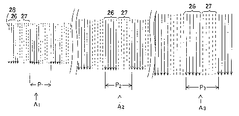
Fig. 1 is a top view illustrative of the writing process
where the pitch of grooves 26 or strips 27 is linearly or
nonlinearly increased or decreased depending on the position
CA 02580820 2007-03-20
-11-
of grooves 26 in the direction perpendicular to groove 26. A
region A1 sampled out of the left end of the phase mask 21 has
a groove pitch P1 with respect to groove 26 or strip 27, a
region A2 sampled out of the center of the phase mask 21 has a
pitch P2 with respect to groove 26 or strip 27, and a region
A3 sampled out of the right end of the phase mask 21 has a
pitch P3 with respect to groove 26 or strip 27. Here assume
P1 < P2 < P3. The substrate of the phase mask 21 is scanned
out sequentially by electron beam scanning lines 28 in the
raster scan mode, from top to bottom and from left end to
right end, thereby writing each groove 26 thereon. In this
case, one groove 26 is written by the same number of scanning
lines at all regions A1r A2 and A3 (5 scanning lines in the
illustrated embodiment). At the position where strip 27 is
to be written, as many as scanning lines are blanked. For
this reason, the inter-central distance of the scanning lines
28 changes with regions A1, A2 and A3 depending on pitches P1,
P2 and P3.
When such a writing process is used, there is a
possibility that unexposed portions may remain after
development of an electron beam resist (see Fig. 6), because
the areas of the portions between the scanning lines 28 and
unexposed to electron beams to write grooves 26 vary with
regions A1r A2 and A3. However, this offers no problem at
all, because the unexposed resist is actually removed upon
development of the regions corresponding to the scanning
lines 28.
CA 02580820 2007-03-20
-12-
As explained above, the pitch of grooves 26 or strips 27
on the phase mask 21 is linearly or nonlinearly increased or
decreased depending on their position in the direction
perpendicular to the grooves 26, so that the width of grooves
26 or strips 27 can be increased or decreased depending on
such a change. By use of the writing process where one
groove 26 is written in the raster scan mode using the same
number of scanning lines at any position, it is possible to
write the desired pattern all over the surface of the
substrate of the phase mask 21 with electron beams. The
writing data needed for this are only two, i.e., fundamental
pattern data concerning one pitch of the mask 21, and a
reduced scale variation function for the fundamental pattern
data, which corresponds to a pitch variation function
depending on the position of groove 26 in the direction
perpendicular to the groove 26.
Fig. 3 is a top view of the writing process wherein the
pitch of grooves 26 or strips 27 are linearly or nonlinearly
increased or decreased depending on their position in a
direction of each groove 26. An region B1 of a phase mask
(21) substrate at its lowermost end along the direction of
groove 26 has a pitch P1 with respect to groove 26 or strip
27, a region B2 positioned just above B1 along the direction
of groove 26 has a pitch P2 with respect to groove 26 or strip
27, a region B3 positioned just above B2 along the direction
of groove 26 has a pitch P3 with respect to groove 26 or strip
27, ===, a region B7 of the phase mask (21) substrate
positioned just below its uppermost end along the direction
CA 02580820 2007-03-20
-13-
of groove 26 has a pitch P7 with respect to groove 26 or strip
27, and a region B8 at the uppermost end along the direction
of groove 26 has a pitch P8 with respect to groove 26 or strip
27. Here assume P1 > P2 > P3 >... > P7 > P8. One region Bn
(n = 1 to 7) is scanned with electron beams in the raster
scan mode, from top to bottom, to write groove 26 thereon.
Then, the next region Bn+l is scanned in the same manner as
mentioned. In this way, all regions B1 to B8 are scanned to
write grooves 26 thereon. It is here to be understood that
at all regions B1 to B8, one groove 26 is written with the
same number of scanning lines (5 scanning lines in the
illustrated embodiment). At a position where strip 27 is to
be written, the same number of scanning lines are blanked
during scanning. For this reason, the inter-central distance
of the scanning lines 28 varies with regions B1 to Bg
depending on pitches P1 to P8.
When such a writing process is used, there is a
possibility that unexposed portions may remain after
development of an electron beam resist (see Fig. 6), because
the areas of the portions between the scanning lines 28 and
unexposed to electron beams to write grooves 26 vary with
regions B1 to Bg. However, this offers no problem at all,
because the unexposed resist is actually removed upon
development of the regions corresponding to the scanning
lines 28.
As explained above, the pitch of grooves 26 or strips 27
on the phase mask 21 is linearly or nonlinearly increased or
decreased depending on their position in the direction
CA 02580820 2007-03-20
-14-
perpendicular to grooves 26, so that the width of grooves 26
or strips 27 can be increased or decreased depending on such
a change. By use of the writing process where one groove 26
is written in the raster scan mode using the same number of
scanning lines at any position, it is possible to write the
desired pattern all over the surface of the substrate of the
phase mask 21 with electron beams. The writing data needed
for this are only two, i.e., fundamental pattern data
concerning one pitch of the mask 21, and a reduced scale
variation function for the fundamental pattern data, which
corresponds to a pitch variation function depending on the
position of groove 26 in the direction perpendicular to the
groove 26.
The phase mask 21 where the pitch of grooves 26 or
strips 27 is linearly or nonlinearly increased or decreased
depending on their position in the direction of grooves 26,
as shown in Fig. 3, is suitable for the fabrication of a
grating used to make a Bragg diffraction grating in an
optical fiber, wherein the pitch thereof is linearly or
nonlinearly increased or decreased depending on the groove
position in the groove direction. Such a grating, for
instance, is preferably used to allow the reflection
wavelength of an optical fiber to vary in a position-
dependent manner. The grooves 26 and strips 27 on such a
phase mask 21 extend in a direction perpendicular to the
sheet surface on which Fig. 7(a) is drawn, so that the pitch
of the grating to be fabricated in an optical fiber 22 can be
selectively controlled by control of the position of the
CA 02580820 2007-03-20
-15-
grooves and strips in the direction perpendicular to the
sheet surface.
In the writing process shown in Fig. 3, the above
reduced scale variation function should be set such that the
amount of displacement between groove 26 on one region Bn and
groove 26 on the next region Bn+1 in the direction
perpendicular to groove 26 is within the width of one groove
26 even at the horizontal outermost ends, as shown in Fig. 4.
Although it is acceptable that writing is carried out while
one region Bn is in contact with the adjacent region Bn+1, it
is preferable that both the regions overlap to some extent
because the grooves 26 or straps 27 are smoothly joined to
each other.
Fig. 5 is a schematic illustrating the writing process
of the invention as compared with a prior art writing
process. Fig. 5 corresponds to the writing process in Fig.
1, and corresponds nearly to the writing process in Fig. 3 as
well. When the pitch of grooves 26 or strips 27 on the phase
mask 21 are linearly or nonlinearly increased or decreased in
a position-dependent manner, the prior art writing process
requires an enormous amount of writing data, and so a number
of writing pattern data A, B, C, D, E, ===, V, W, X, Y and Z,
as shown in Fig. 5(b), must be kept on hand. This is
contrast to the writing process of the invention, for which
only fundamental pattern data A is needed together with a
reduced scale variation function P(x) corresponding to a
position x (the position of groove 26 in the direction
perpendicular to groove 26 in Fig. 1, and the position of
CA 02580820 2007-03-20
-16-
groove 26 in the direction of groove 26 in Fig. 3). For
writing, only the use of A x R(x) = An and the fundamental
pattern data A scaled down depending on the position is
needed, as shown in Fig. 5(a). Thus, the amount of writing
data can be reduced so that writing can be facilitated. In
Fig. 1 and Fig. 5(a), the writing range in the vertical
direction varies with position because the reduced scale is
varied not only in the horizontal direction but in the
vertical direction as well. When the reduced scale is varied
in the horizontal direction alone depending on the position
(as required in Fig. 3 in particular), the writing range in
the vertical direction can be kept constant at every
position.
For instance, when one-pitch writing data comprising a
0.125-pm address unit and 10 scanning lines are provided as
the fundamental pattern data, the reduced scale is given by
(desired grating pitch)/(0.125 x 10). Using this reduced
scale and the fundamental pattern data with an electron beam
writing system, grooves are written on an electron beam
resist coated on the transparent substrate. One specific
embodiment of the phase mask fabrication method of the
invention using such a writing process will now be explained.
Figs. 6(a) to 6(h) are sectional views of steps of
fabricating a phase mask according to the invention. Here,
reference numeral 10 stand for a phase mask blank, 11 a
quartz substrate, 12 a chromium thin film, 12A a chromium
thin film pattern, 12B a chromium thin film opening, 13 an
electron beam resist, 13A a resist pattern, 13B a resist
CA 02580820 2007-03-20
-17-
opening, 14 an electron beam, 21 a phase mask, 26 a groove,
and 27 a strip.
As shown in Fig. 6(a), the chromium thin film 12 of 150
A in thickness was first formed on quartz substrate 11 to
prepare the blank 10. The chromium thin film 12 is useful to
prevent charging-up during irradiation of electron beam
resist 13 with electron beams 14 at the later step, and acts
as a mask in making grooves 26 in the quartz substrate. The
thickness of chromium thin film 12 is also important in view
of resolution upon chromium thin film etching, and so is
preferably in the range of 100 to 200 A.
Then, the electron resist 13, e.g., an electron resist
RE5100P (made by Hitachi Kasei K.K.) was coated on chromium
thin film 12 to a thickness of 400 nm and dried, as shown in
Fig. 6(b).
Following this, an electron beam writing system MEBESIII
(made by ETEC) was used to expose electron beam resist 13 to
electron beams 14 at an exposure of 1.2 pC/cm2, as shown in
Fig. 6(c), while, as explained with reference to Figs. 1 and
3, the pitch of grooves 26 was linearly increased, from left
to right or in a direction perpendicular to the drawing
sheet, depending on their position in the direction
perpendicular to grooves 26 or their position in the
direction of grooves 26, and the widths of grooves 26 and
strips 27 were increased with such a change. In this step,
the width between the electron beams 14 was sequentially
controlled in such a way that one groove was always written
CA 02580820 2007-03-20
-18-
with five scanning lines at every position in the raster scan
mode.
After exposure to the electron beams, baking (post
exposure baking or PEB) was carried out at 90 C for 5
minutes. Thereafter, the electron beam resist 13 was
developed with TMAH (tetramethylammonium hydroxide) at a
concentration of 2.38% to form such a desired resist pattern
13A as shown in Fig. 6(d). It is here to be noted that the
post exposure baking (PEB) was performed to selectively
enhance the sensitivity of the portions irradiated with
electron beams 14.
Subsequently, dry etching was carried out using a CH2C12
gas while the resist pattern 13A was used as a mask to form
such a chromium thin film pattern 12A as shown in Fig. 6(e).
As shown in Fig. 6(f), the quartz substrate 11 was then
etched to a depth of exactly 240 nm using a CF4 gas while the
chromium thin film pattern 12A was used as a mask. Depth
control was carried out by control of etching time, and
etching could be performed while the thickness was controlled
to the range of 200 to 400 nm.
After this, the resist pattern 13A was stripped out with
sulfuric acid of 700C, as shown in Fig. 6(g). Then, the
chromium thin film pattern 12A was etched out with an
ammonium solution of cerium (IV) nitrate, as shown in Fig.
6(h). Finally, the product was washed to obtain a finished
line-and-space (or strip 27-and-groove 26) phase mask 21
having a depth of 240 nm and a pitch changing linearly from
CA 02580820 2007-03-20
-19-
0.85 pm to 1.25 pm in the direction perpendicular to grooves
26 or in the direction of grooves 26.
While the optical fiber-processing phase mask and its
fabrication method have been explained with reference to some
preferred embodiments, it is to be understood that the
invention is in no sense limited thereto and so many
modification may be made thereto. While the invention has
been explained with reference to the raster scan type
electron beam writing system, it is also to be understood
that the invention may be carried out using a vector scan or
other type electron beam writing system.
POSSIBILITY OF UTILIZATION IN INDUSTRY
As can be obvious from the foregoing explanation, the
optical fiber-processing phase mask of the invention and its
fabrication method enable a diffraction grating with a
varying pitch to be made in an optical fiber. This is
because the phase mask of the invention comprises a plurality
of juxtaposed patterns, each having a linearly or.nonlinearly
increasing or decreasing pitch, with a constant width ratio
of grooves and strips. If writing data concerning a
fundamental pattern comprising one groove and one strip are
multiplied by a reduced scale ratio, it is then possible to
obtain writing data concerning the entire repetitive pattern
of grooves and strips located in a grating from with a pitch
varying depending on their position in the direction
perpendicular to grooves or in the direction of grooves.
Thus, some considerable reductions in the amount of writing
data are achieved to make pattern formation easy. This
CA 02580820 2007-03-20
-20-
process also enables a phase mask to be fabricated at any
desired pitch.