Language selection

Search

Patent 2581260 Summary

Third-party information liability

Some of the information on this Web page has been provided by external sources. The Government of Canada is not responsible for the accuracy, reliability or currency of the information supplied by external sources. Users wishing to rely upon this information should consult directly with the source of the information. Content provided by external sources is not subject to official languages, privacy and accessibility requirements.

Claims and Abstract availability

Any discrepancies in the text and image of the Claims and Abstract are due to differing posting times. Text of the Claims and Abstract are posted:

  • At the time the application is open to public inspection;
  • At the time of issue of the patent (grant).
(12) Patent Application: (11) CA 2581260
(54) English Title: SURFACE ACOUSTIC WAVE GAS SENSOR WITH SENSITIVE GETTER LAYER AND PROCESS FOR ITS MANUFACTURE
(54) French Title: CAPTEUR DE GAZ A ONDE ACOUSTIQUE DE SURFACE COMPRENANT UNE COUCHE DE GETTER SENSIBLE ET PROCEDE PERMETTANT DE FABRIQUER CE CAPTEUR
Status: Dead
Bibliographic Data
(51) International Patent Classification (IPC):
  • G01N 29/02 (2006.01)
  • C22C 16/00 (2006.01)
  • G01N 29/22 (2006.01)
  • G01N 29/24 (2006.01)
  • G01N 29/30 (2006.01)
  • G01N 33/00 (2006.01)
(72) Inventors :
  • AMIOTTI, MARCO (Italy)
(73) Owners :
  • SAES GETTERS S.P.A. (Italy)
(71) Applicants :
  • SAES GETTERS S.P.A. (Italy)
(74) Agent: GOWLING LAFLEUR HENDERSON LLP
(74) Associate agent:
(45) Issued:
(86) PCT Filing Date: 2005-10-17
(87) Open to Public Inspection: 2006-04-27
Availability of licence: N/A
(25) Language of filing: English

Patent Cooperation Treaty (PCT): Yes
(86) PCT Filing Number: PCT/IT2005/000605
(87) International Publication Number: WO2006/043299
(85) National Entry: 2007-03-21

(30) Application Priority Data:
Application No. Country/Territory Date
MI2004A 002017 Italy 2004-10-22

Abstracts

English Abstract


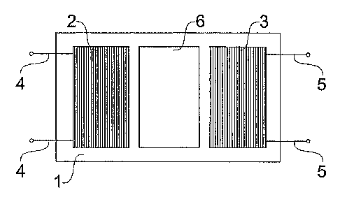
Surface acoustic wave gas sensor, in particular a vacuum or hydrogen sensor,
comprising a piezoelectric substrate (1) on which at least one layer of a gas-
sensitive material (6) is arranged between two inter-digital transducers (2,
3) and comprises a getter material, so that the molecules sorbed by this
getter material can vary the frequency of a signal transmitted between the two
transducers (2, 3). The present invention also relates to a process for
manufacturing this sensor.


French Abstract

L'invention concerne un capteur de gaz à onde acoustique de surface, en particulier un capteur d'hydrogène ou un capteur de dépression, comprenant un substrat (1) piézoélectrique sur lequel est appliquée au moins une couche de matériau (6) sensible aux gaz intercalée entre deux transducteurs (2, 3) interdigités, et comprenant un getter, de telle manière que les molécules sorbées par le getter produisent une modification de la fréquence d'un signal transmis entre les deux transducteurs (2, 3). La présente invention se rapporte également à un procédé permettant de fabriquer ce capteur.

Claims

Note: Claims are shown in the official language in which they were submitted.


-5-

CLAIMS


1. A sensor comprising a piezoelectric substrate (1) on which is present at
least
one first layer (6) of a gas-sensitive material comprising a getter material
arranged
between two inter-digital transducers (2, 3), characterized by further
comprising, over
said first layer, a second layer (7) of a material permeable to one or more
determined
gases, being also arranged between said two inter-digital transducers, so that
the
molecules sorbed by the getter material can vary the frequency of a signal
transmitted
between the two transducers (2, 3).

2. A sensor according to claim 1, wherein said sensitive layer (6) is a getter
film.

3. A sensor according to claim 2, wherein said getter material comprises a
metal
chosen among zirconium, titanium, niobium, tantalum, vanadium or alloys of
these
metals or of these and one or more other elements, chosen among chromium,
manganese, iron, cobalt, nickel, aluminum, yttrium, lanthanum and rare earths.

4. A sensor according to claim 3, wherein said getter material comprises Ti-V,

Zr-V, Zr-Fe, Zr-Al and Zr-Ni binary alloys, and Zr-Mn-Fe, Zr-V-Fe and Zr-Co-MM

ternary alloys, where MM is a mixture of yttrium, lanthanum and rare earths.

5. A sensor according to claim 2, wherein said getter film has a thickness
comprised between 0,5 and 5 µm.

6. A sensor according to claim 1, wherein said permeable layer (7) comprises a

noble metal or an alloy thereof.


7. A sensor according to claim 6, wherein said permeable layer (7) comprises
palladium or platinum.

8. A sensor according to claim 1, wherein said permeable layer (7) has a
thickness comprised between 50 and 500 nm.

9. A sensor according to claim 1, further comprising a resistive device (8)
suitable for being heated at an activation temperature for getter materials,
arranged
between the piezoelectric substrate (1) and the gas-sensitive layer (6).


10. A sensor according to claim 1, further comprising a second pair of inter-
digital
transducers (2', 3') arranged on the piezoelectric substrate (1), said first
layer (6) and
second layer (7) being arranged only between the first pair of inter-digital
transducers


-6-

(2, 3).

11. A sensor according to claim 1, further comprising at least one antenna (9)
for
receiving and/or transmitting radio signals connected to at least one inter-
digital
transducer (2).

12. A sensor according to claim 1, wherein said sensor is a vacuum sensor.

13. A sensor according to claim 1, wherein said sensor is a hydrogen sensor.


14. A process for manufacturing gas sensors, comprising the following
operating
steps:
- applying a plurality of pairs of inter-digital transducers (2, 3; 2', 3')
onto a wafer
(1) of a piezoelectric substrate;
- arranging onto said wafer a mask provided with calibrated openings, so that
these openings are comprised between a pair of inter-digital transducers (2,
3);
- depositing onto the wafer by means of sputtering through said mask a layer
(6)
of a gas-sensitive material comprising a getter material;
- arranging onto the wafer a mask provided with calibrated openings, so that
these
openings are comprised between a pair of inter-digital transducers;
- depositing onto the wafer through said mask by means of sputtering a layer
(7)
of a material permeable to one or more determined gases.

15. A process according to claim 14, wherein only one mask is used and the
steps
of depositing said layer of a gas-sensitive material and of depositing said
layer of a
material permeable to gases are carried out using the same mask.

16. A process according to claim 14, wherein a plurality of resistive devices
are
arranged on the wafer between the pairs of inter-digital transducers before
depositing
onto the wafer the layer of gas-sensitive material.

17. A process according to claim 14 or 15, wherein said deposition steps are
carried out by means of sputtering.


Description

Note: Descriptions are shown in the official language in which they were submitted.


14-12-2006 CA 02581260 2007-03-21 IT20050006C
SURFACE ACOUSTIC WAVE GAS SENSOR WITH SENSITIVE GETTER LAYER
AND PROCESS FOR ITS MANUFACTURE

The present invention relates to a gas sensor embodying the surface acoustic
wave
or SAW technology, in particular a vacuum or hydrogen sensor. The present
invention
also relates to a process for manufacturing this sensor.
Known gas sensors comprise a SAW device wherein a layer of a material
sensitive to a determined gas is arranged on the piezoelectric substrate of
the SAW
device between its inter-digital transducers.
Document "Development of a SAW gas sensor for monitoring SO2 gas", Sensors
and Actuators A 64 (1998) of Y. J. Lee discloses a sensitive layer of cadmium
sulphide
for measuring concentrations of SOz.
US 5583282 discloses a sensor comprising a piezoelectric substrate on which at
least one layer of a gas-sensitive material is arranged between two inter-
digital
transducers, the gas-sensitive material comprising a getter material.
US 5592215 discloses a sensitive layer of gold, silver or copper for measuring
concentrations of mercury.
US 2004/0107765 discloses a sensitive layer of cellulose nitrate for measuring
concentrations of acetone, benzene, dichloroethane, ethanol or toluene.
However, said sensors cannot measure concentrations of simple molecules, or
even measure the vacuum level in an evacuated environment, due to the
relatively low
sensitivity of their sensitive layer.
It is therefore an object of the present invention to provide a SAW sensor
free
from said disadvantages. Said object is achieved with a sensor and a
manufacturing
process, the main features of which are disclosed in claims I and 19,
respectively, while
other features are disclosed in the remaining claims.
Thanks to the getter material included in the gas-sensitive layer, the sensor
according to the present invention can be employed as a vacuum sensor or as a
sensor
for simple molecules, for example hydrogen, if the sensitive layer is covered
by a
particular layer of a material permeable to these molecules. In particular,
the sensor can
be arranged in an evacuated system already provided with a getter, so as to
detect when
AMENDED SHEET


CA 02581260 2007-03-21

14-12-2006 IT20050006C
-2-
the latter must be regenerated.
A resistive device can be arranged between the piezoelectric substrate and the
gas-
sensitive layer for activating and/or regenerating the getter material at a
high
temperature without damaging the transducers with the heat.
The sensitive layer is preferably made of a thin getter film applied by means
of
Physical Vapor Deposition or "PVD", commonly indicated also as "sputtering",
so as to
simplify the sensor manufacturing and keep its sensitivity as much constant as
possible,
thus improving its measurement precision.
For further improving the measurement precision of the sensor, a second pair
of
inter-digital transducers can be arranged on the piezoelectric substrate with
the sensitive
layer arranged only between the first pair of transducers.
For manufacturing the sensor, masks provided with calibrated openings can be
employed for depositing layers having precise dimensions onto a wafer already
provided with more pairs of transducers, so as to reduce the manufacturing
times and
costs and to reproducibly keep a high sensor quality.
This technique is known e.g. from EP-A-0936734, which discloses a process for
manufacturing a SAW device comprising the steps of sputtering tantalum-
aluminum
layers and using masks to obtain the sensor pattern.
Further advantages and features of the sensor and the manufacturing process
according to the present invention will become clear to those skilled in the
art from the
following detailed and non-limiting description of some embodiments thereof
with
reference to the attached drawings, wherein:
- figure 1 shows a top view of a first embodiment of the sensor,
- figure 2 shows a partial cross-section view of a second embodiment of the
sensor;
- figure 3 shows a partial cross-section view of a third embodiment of the
sensor;
- figure 4 shows a top view of a fourth embodiment of the sensor; and
- figure 5 shows a top view of a fifth embodiment of the sensor.
Referring to figure 1, it is seen that the gas sensor according to the ,Ãr4A,
of thq invention comprises in a known way a piezoelectric substrate 1 on
which are arranged two inter-digital transducers 2, 3 provided with one or
more input or
output conductive lines 4, 5 for the wired or wireless connection to electric
and/or


CA 02581260 2007-03-21

14-1 2-2006 --I120050006C
Sll)p, Q ~{P~ l_r~O~fet~'~ >
.~
z
electronic control devices. At least one layer 6 of a gas-sensitive
materialtiis arranged on
the surface of substrate 1 comprised between transducers 2, 3,0

,
_m~ so that the molecules sorbed by this getter material can vary the
frequency of
an electric signal transmitted between transducers 2, 3. The vacuum level in
an
evacuated environment can thus be measured through a suitable calibration
curve by


CA 02581260 2007-03-21
14 12 2006 IT20050006i
-3-
arranging the sensor in this environment and by measuring said frequency
variation.

In particular, the sensitive layer 6 is a getter film which has a thickness
comprised
between 0,5 and 5 m (micrometers) and is applied onto substrate 1 by
sputtering. The
getter material can comprise metals such as zirconium, titanium, niobium,
tantalum,
vanadium or alloys of these metals or of these and one or more other elements,
chosen
among chromium, manganese, iron, cobalt, nickel, aluminum, yttrium, lanthanum
and
rare earths. Ti-V, Zr-V, Zr-Fe, Zr-Al and Zr-Ni binary alloys, and Zr-Mn-Fe,
Zr-V-Fe and
Zr-Co-MM ternary alloys (where MM represents mischmetal, a commercial mixture
of
yttrium, lanthanum and rare earths) proved to be particularly suitable,
especially in the
following compositions by weight: Zr 70% - V 24,6 % - Fe 5,4% or Zr 84% - Al
16%.
Referring to figure 2, it is seen that ~~'~ ~~~e~the invention a layer
7 of a material selectively permeable only to one or some determined gasses is
arranged over sensitive layer 6, so that the sensor can measure concentrations
of the gas permeating

through the permeable layer 7, also in a non-evacuated environment. In
particular, the
permeable layer 7 has a thickness comprised between 50 and 500 nm (nanometers)
and
comprises a noble metal, preferably palladium or platinum or an alloy thereof,
so as to let
only hydrogen molecules permeate, which are thus sorbed by the getter material
of the
sensitive layer 6.
gecoN+d
Referring to figure 3, it is seen that in a444 embodiment of the invention a
resistive device 8 suitable for being heated at an activation temperature for
getter
materials, in particular comprised between 300 and 450 C, is arranged between
substrate 1 and the sensitive layer 6. The resistive device 8 can be heated by
means of a
current flow, for example by powering the same through suitable electric
feedthroughs
(not shown in the figure), so as to carry out the first activation or the
regeneration of the
getter material of the sensitive layer 6_ In fact, in the case of the hydrogen
sensor, the
heating of the sensitive layer 6 serves for releasing the hydrogen previously
sorbed by
the same.
e,ird
Referring to figure 4, it is seen that in a embodiment of the invention two
pairs of inter-digital transducers 2, 2', 3, 3', each provided with one or
more input or
output lines 4, 4', 5, 5', are arranged side by side on the piezoelectric
substrate 1. The
sensitive layer 6 is arranged only between two inter-digital transducers 2, 3,
so that


CA 02581260 2007-03-21

14-12-2006 IT20050006(
-4-
differential measurements of the frequency variation of the electric signals
transmitted
between transducers 2, 2' and 3, 3' can be carried out.
jau r7Ec
Referring to figure 5, it is seen that in a frfth embodiment of the invention
the first
inter-digital transducer 2 is connected to one or more antennas 9 for
receiving and/or
transmitting radio signals from external devices. The second inter-digital
transducer 3 is

not connected to any device, neither by cable nor by radio, and simply
reflects toward
the first transducer 2 the' signal received through the piezoelectric
substrate 1 and
modified by the sensitive layer 6 arranged between transducers 2, 3.
For manufacturing the sensors according to the present invention, a mask is
mechanically aligned and then arranged in contact with a wafer of a
piezoelectric
substrate, on which a plurality of pairs of inter-digital transducers and, if
required, a
plurality of resistive devices are already applied. Said mask is provided with
calibrated
openings having dimensions corresponding to those desired for the sensitive
layers,
which are then deposited onto the wafer by means of sputtering. For
manufacturing
hydrogen sensors, it is sufficient to apply permeable layers onto the
sensitive layers
deposited on the wafer, again by means of sputtering through a mask. After the
deposition of the sensitive layers and, if any, of the permeable layers, the
wafer is cut by
means of mechanic or laser cut for obtaining a plurality of sensors ready for.
use.
Further variations and/or additions may be made by those skilled in the art to
the
hereinabove described and illustrated embodiments of the invention while
remaining
within the scope of the same invention.

Representative Drawing
A single figure which represents the drawing illustrating the invention.
Administrative Status

For a clearer understanding of the status of the application/patent presented on this page, the site Disclaimer , as well as the definitions for Patent , Administrative Status , Maintenance Fee  and Payment History  should be consulted.

Administrative Status

Title Date
Forecasted Issue Date Unavailable
(86) PCT Filing Date 2005-10-17
(87) PCT Publication Date 2006-04-27
(85) National Entry 2007-03-21
Dead Application 2010-10-18

Abandonment History

Abandonment Date Reason Reinstatement Date
2009-10-19 FAILURE TO PAY APPLICATION MAINTENANCE FEE

Payment History

Fee Type Anniversary Year Due Date Amount Paid Paid Date
Registration of a document - section 124 $100.00 2007-03-21
Application Fee $400.00 2007-03-21
Maintenance Fee - Application - New Act 2 2007-10-17 $100.00 2007-09-24
Maintenance Fee - Application - New Act 3 2008-10-17 $100.00 2008-09-23
Owners on Record

Note: Records showing the ownership history in alphabetical order.

Current Owners on Record
SAES GETTERS S.P.A.
Past Owners on Record
AMIOTTI, MARCO
Past Owners that do not appear in the "Owners on Record" listing will appear in other documentation within the application.
Documents

To view selected files, please enter reCAPTCHA code :


To view images, click a link in the Document Description column. To download the documents, select one or more checkboxes in the first column and then click the "Download Selected in PDF format (Zip Archive)" or the "Download Selected as Single PDF" button.

List of published and non-published patent-specific documents on the CPD .

If you have any difficulty accessing content, you can call the Client Service Centre at 1-866-997-1936 or send them an e-mail at CIPO Client Service Centre.


Document
Description 
Date
(yyyy-mm-dd) 
Number of pages   Size of Image (KB) 
Claims 2007-03-21 2 88
Abstract 2007-03-21 1 63
Description 2007-03-21 5 216
Drawings 2007-03-21 2 52
Representative Drawing 2007-05-30 1 13
Cover Page 2007-05-31 1 46
Prosecution-Amendment 2007-03-21 3 89
PCT 2007-03-21 14 619
Assignment 2007-03-21 5 138