Note: Descriptions are shown in the official language in which they were submitted.
CA 02581553 2007-03-14
=
AUTO-TUNED RFID READER ANTENNA
TECHNICAL FIELD
The present invention relates generally to readers for radio frequency
identification systems, more particularly, to an auto-tuning circuit for use
with an
antenna of a reader.
BACKGROUND OF THE INVENTION
Radio frequency identification (RFID) systems typically include at least one
reader and a plurality of transponders, which are commonly termed credentials,
cards, tags, or the like. The transponder may be an active or passive radio
frequency communication device which is directly attached to or embedded in an
article to be identified or otherwise characterized by the reader.
Alternatively, the
transponder may be embedded in a portable substrate, such as a card or tag,
carried by a person or an article to be identified or otherwise characterized
by the
reader. An active transponder is powered up by its own internal power supply,
such
as a battery, which provides the operating power for the transponder
circuitry. In
contrast, a passive transponder is characterized as being dependent on the
reader
for its power. The reader "excites" or powers up the passive transponder by
transmitting excitation signals of a given frequency into the space
surrounding the
reader, which are received by the transponder and provide the operating power
for
the circuitry of the recipient transponder.
Communication between the reader and transponder is enabled by
cooperative resonant circuits which are provided in each reader and
transponder.
The resonant circuit of a reader includes an inductor, typically in the form
of an
antenna, which magnetically couples to the inductor in the resonant circuit of
a
compatible transponder through mutual inductance. The resonant circuit of the
transponder correspondingly includes an inductor which magnetically couples to
the
inductor in the resonant circuit of the reader through mutual inductance.
Communication is initiated when a transponder is proximally positioned
1
CA 02581553 2007-03-14
relative to the reader. The reader has a power supply which conveys a current
to
the reader resonant circuit causing the reader antenna to produce an
excitation
signal in the form of an electromagnetic field. The excitation signal couples
to the
antenna of the proximally-positioned transponder through mutual inductance and
the
excitation signal powers and clocks the transponder circuitry initiating
operation of
the transponder.
Transponder operation comprises generation of a response signal at a
specified frequency and transmission of the transponder response signal back
to the
reader. In particular, the transponder resonant circuit receives a current in
response
to the excitation signal which causes the transponder antenna to produce a
response signal in the form of an electromagnetic field. The response signal
couples to the reader antenna through mutual inductance in substantially the
same
manner as described above with respect to coupling of the excitation signal to
the
transponder antenna.
The transponder typically employs frequency or amplitude modulation of the
response signal to encode data stored in the memory of the transponder
circuitry
into the response signal. When the response signal couples to the reader
antenna,
a corresponding current is induced in the reader antenna at the specified
frequency.
The reader processes the induced current to read the data encoded in the
response
signal. The resulting data may be communicated to an output device, such as a
display, printer, or storage device, and simultaneously, or alternatively,
communicated to a host computer, if a host computer is networked into the RFID
system.
An important operating parameter of the reader is the range of the reader
when communicating with a transponder. The range of the reader is inter alia
strongly affected by the strength of the electromagnetic field generated by
the reader
resonant circuit. In order to generate a field strength which provides the
reader with
adequate range, the designer of the reader must properly specify a resonant
circuit
which is appropriately tuned to a predetermined frequency for the desired
application
of the RFID system.
2
CA 02581553 2007-03-14
Another important operating parameter of the reader is antenna impedance.
It is desirable that the impedance of the antenna in the reader of an RFID
system be
specified to match the impedance of the antenna driver. However, the impedance
of
the reader antenna is often altered by the characteristics of the operating
environment in which the reader resides. In a typical case where the reader is
mounted in a fixed location on a support structure, the impedance of the
reader
antenna is susceptible to the materials of the mounting location and other
objects
within the operating environment. For example, if the mounting location of the
reader is in an operating environment which includes nearby metal, the metal
can
alter the effective impedance of the resonant circuit, thereby detuning the
resonant
circuit from the predetermined frequency and dramatically reducing the range
of the
reader. Additionally, the impedance of the reader antenna can be disturbed
during
the antenna or reader fabrication process resulting in a detuned resonant
circuit.
One means of overcoming the above-mentioned problems is to specifically
tune each individual reader antenna for its intended operating environment.
For
example, the reader antenna may be individually tuned using component
selection
procedures during the reader fabrication process so that the impedance of the
reader antenna matches the impedance of the antenna driver when installed in
the
intended operating environment. However, specific component selection during
production is labor intensive and requires a high level of training and
supervision,
which are oftentimes cost prohibitive.
Alternatively, reader antennas may be tuned to a frequency between
specified extremes to achieve consistent performance within a number of
different
operating environments. For example, the mounting location of the reader may
reasonably be expected to consist of either drywall or a steel junction box.
Rather
than optimize the reader for one or the other of these two mounting locations,
the
antenna tuning is compromised so that antenna performance is consistent
(although
sub-optimal) in either operating environment. Although this alternative
appears
attractive, in practice the range of potential operating environments is
typically so
varied that it is not practical to optimize tuning for one environment over
others. The
3
: _ ._ ...... _. ... . _,.2.. _ ..:w....,_ .v F.~...- . ._ ..,_., . ,
.,w.::..... _ ..... .. .. .. _ ..1 r ,,., _ .., .3 ., ...e. -. 1. .... -, a, ,
. - .. .. . .. .. .. . ._.. .
CA 02581553 2007-03-14
full range of possible operating environments can have a drastic impact on
antenna
performance, especially when a reader is required to support multiple radio
frequency (RF) protocols and transponder types. Compromising the antenna
tuning
between extremes results in reduced performance and can void the performance
of
some protocols and transponder types altogether.
The present invention recognizes a need for a reader of an RFID system
which is adaptable to variations in its antenna performance caused by
different
operating environments and/or variations in values of the antenna fabrication
parameters. Accordingly, it is generally an object of the present invention to
provide
an RFID system having a reader which exhibits satisfactory performance
characteristics while adjusting to variations in a given system operating
environment.
More particularly, it is an object of the present invention to provide a
reader
achieving a uniformly satisfactory level of performance when the reader is
employed
in different operating environments. It is another object of the present
invention to
provide a reader which automatically retunes itself to maintain a desired
performance level in response to variations in the operating environment of
the
reader. These objects and others are accomplished in accordance with the
invention described hereafter.
SUMMARY OF THE INVENTION
The present invention is a reader for an RFID system. The reader comprises
an antenna assembly, a signal driver and a controller. The antenna assembly
includes an antenna tuning circuit and an antenna coupled to the antenna
tuning
circuit. The antenna has an antenna impedance and the signal driver has a
signal
driver impedance. The antenna tuning circuit includes a variable capacitance
circuit
having a variable capacitance. The signal driver is coupled to the antenna
assembly
to apply a drive signal to the antenna. The controller is coupled to the
antenna
assembly to determine a difference between the antenna impedance and the
signal
driver impedance and to set the variable capacitance to a set capacitance
value
which reduces the difference between the impedances.
4
........ ... .. . . . . . .. . . ...... . ...,......,... ......_..._: .,. .._.
.__ :....:sw r. ...,....-... ... , ., . ... .... . ..I i...:,.....-..,.
..,...,..., . ...,.,,.......I....... ., ...:., ,..... ...._ ..,..... . . ..
_.... .. .....
CA 02581553 2007-03-14
In accordance with one embodiment, the reader further comprises a variable
voltage source coupled between the controller and the variable capacitance
circuit to
apply a tuning bias signal to the variable capacitance circuit. The tuning
bias signal
has a biasing voltage value selected to reduce the difference between the
impedances. In accordance with another embodiment, the antenna tuning circuit
further includes a fixed value capacitance circuit having one or more fixed
value
capacitors coupled in parallel to the antenna and/or a fixed value capacitance
circuit
having one or more fixed value capacitors coupled in series to the antenna. In
accordance with yet another embodiment, the variable capacitance circuit
comprises
one or a plurality of paraliely connected variable capacitance elements. The
variable
capacitance circuit alternately comprises a fixed value capacitor connected in
series
to one or a plurality of parallely connected variable capacitance elements.
The reader preferably further comprises a radio frequency transmissive
housing at least partially enclosing the antenna assembly and a radio
frequency
reflective baseplate coupled to the housing to reduce susceptibility of the
antenna to
variations caused by objects in an operating environment of a reader. The
housing
is preferably fabricated from a plastic and the baseplate is preferably
fabricated from
a metal.
In an alternate characterization, the present invention is a method comprising
conveying a drive signal from a signal driver to an antenna assembly. The
antenna
assembly includes an antenna tuning circuit coupled to an antenna. The antenna
has an antenna impedance, the signal driver has a signal driver impedance, and
the
antenna tuning circuit has a variable capacitance. A difference between the
antenna
impedance and the signal driver impedance is determined and the variable
capacitance is set at a set capacitance value to reduce the difference. In one
embodiment, the method further comprises generating a tuning bias signal
having a
biasing voltage value. The tuning bias signal is applied to the antenna tuning
circuit
to set the variable capacitance at the set capacitance value.
In an another characterization, the present invention is a method comprising
selecting a set capacitance value of an antenna tuning circuit having variable
5
,.. ,..
_ . _., . ,.~. . a
CA 02581553 2007-03-14
capacitance. The set capacitance value is selected by ranging an antenna
operating
parameter correlated to the variable capacitance through a progression of
antenna
operating parameter values. The set capacitance value of the antenna tuning
circuit
is set to reduce an imbalance between an impedance of an antenna coupled to
the
antenna tuning circuit and an impedance of a signal driver a applying drive
signal to
the antenna. The imbalance is preferably due to variations in an operating
environment of the antenna or variations in values of an antenna fabrication
parameter of the antenna.
In accordance with one embodiment, the method further comprises
determining values of a circuit operating parameter of a circuit coupled to
the
antenna while ranging the values of the antenna operating parameter. The
values of
the antenna operating parameter are preferably correlated to the values of the
circuit
operating parameter.
In accordance with another embodiment, the method further comprises
setting the antenna operating parameter to an antenna value correlated to the
set
capacitance value using a correlation between the antenna operating parameter
values and the circuit operating parameter values.
A preferred antenna operating parameter is a biasing voltage of a tuning bias
signal applied to the antenna tuning circuit. A preferred circuit operating
parameter
is a magnitude of a drive signal applied to the antenna, a phase across an
inductor
in the circuit, or a voltage magnitude on a terminal of an inductor in the
circuit.
The present invention will be further understood from the drawings and the
following detailed description. Although this description sets forth specific
details, it
is understood that certain embodiments of the invention may be practiced
without
these specific details. It is also understood that in some instances, well-
known
circuits, components and techniques have not been shown in detail in order to
avoid
obscuring the understanding of the invention.
6
CA 02581553 2007-03-14
BRIEF DESCRIPTION OF THE DRAWINGS
Figure 1 is a block diagram of an RFID system including a transponder and a
reader.
Figure 2 is an exploded perspective view of the reader of Figure 1 having
internal circuitry enclosed within a reader housing and baseplate.
Figure 3 is a schematic view of an antenna turning circuit of the reader
antenna assembly of Figure 1.
Embodiments of the invention are illustrated by way of example and not by
way of limitation in the above-recited figures of the drawings in which like
reference
characters indicate the same or similar elements. It should be noted that
common
references to "an embodiment", "one embodiment", "an alternate embodiment", "a
preferred embodiment", or the like herein are not necessarily references to
the same
embodiment.
DESCRIPTION OF PREFERRED EMBODIMENTS
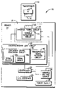
An RFID system is shown in Figure 1 and generally designated 10. The RFID
system 10 comprises a transponder 12 and a reader 14. The transponder 12 is
preferably a passive transponder which does not require an internal power
supply.
The electrical power required to operate the passive transponder 12 is
supplied to
the transponder 12 by electromagnetic energy transmitted from the reader 14,
which
is of a specific frequency and a sufficient strength to power up the
transponder 12.
The transponder 12 comprises a number of functional elements including a
transponder integrated circuit (IC) 16 and a transponder antenna 18. The
transponder IC 16 embodies the processing and memory capabilities of the
transponder 12. The transponder antenna 18 is coupled to the transponder IC 16
and is preferably a conventional coil termed a "dual-function antenna" which
performs both the receiving and transmitting functions of the transponder 12.
Alternatively, two separate receiving and transmitting antennas can be
substituted
for the single "dual function antenna" in the transponder 12. The transponder
12
also preferably includes a transponder capacitor (not shown) coupled to the
7
CA 02581553 2007-03-14
transponder IC 16 and transponder antenna 18. The transponder antenna 18, in
cooperation with the transponder capacitor, defines a transponder LC circuit
having
a tuned resonant frequency which corresponds to the carrier frequency of the
transponder 12.
The transponder 12 shown and described herein is but an example of a type
of transponder having utility in the RFID system 10. It is understood that
practice of
the present invention is not limited to any specific type of transponder, but
is
generally applicable to most conventional types of transponders having utility
in
RFID systems. Thus, for example, the transponder 12 can be selected from
proximity cards, proximity tags, smart cards, or the like.
The reader 14 comprises a number of functional elements including a reader
antenna assembly 20, an exciter/reader (ER) circuit 22, a controller 24, an
input/output (I/O) interface 26, and a power supply 28. The power supply 28
provides electrical operating power to the reader components in a controlled
manner. In accordance with one embodiment, the power supply 28 is coupled to a
finite electrical power source which is self-contained (i.e., internal) within
the reader
14, such as a relatively small portable battery consisting of one or more
disposable
or rechargeable wet or dry cells. Alternatively, the power supply 28 is hard
wired to
an essentially infinite remote electrical power source, such as an electric
utility.
The reader antenna assembly 20 preferably includes an antenna tuning
circuit 30 and a reader antenna 32. The reader antenna 32 is a "dual-function
antenna" which performs both the receiving and transmitting functions of the
reader
14. In particular, the reader antenna 32 receives transponder data signals
from the
external environment and transmits excitation signals into the external
environment.
Although not shown, the present invention alternately encompasses an antenna
assembly having two separate receiving and transmitting antennas,
respectively,
which separately perform the receiving and transmitting functions of the
reader 14.
The antenna tuning circuit 30 includes a variable capacitance circuit 34
coupled to the reader antenna 32. The variable capacitance circuit 34 and
reader
antenna 32 in combination define a reader LC circuit. The reader 14 further
8
CA 02581553 2007-03-14
comprises a variable voltage source 36 coupled between the antenna tunning
circuit
30 and the controller 24. The variable voltage source 36 functions to generate
a
plurality of tuning bias signals in a manner described below. The variable
voltage
source 36 preferably comprises a digital potentiometer or any other suitable
variable
voltage device, such as a microprocessor reference voltage module, a digital
to
analog converter or a variable voltage regulator.
The ER circuit 22 comprises an excitation signal generator circuit 38 and a
transponder signal receiver circuit 40. The excitation signal generator
circuit 38
includes a signal source 38a and a signal driver 38b. The excitation signal
generator circuit 38 generally functions to generate an excitation signal
which the
reader antenna assembly 20 transmits in the form of electromagnetic waves into
the
open space of the operating environment surrounding the reader 14. ' In
particular,
the reader 14 draws electric power from the power source 28 to the signal
source
38a when the transponder 12 is proximally positioned relative to the reader
14. The
signal source 38a produces an signal, which is amplified by the signal driver
38b to
supply an AC drive signal having a high voltage and high current to the reader
antenna assembly 20. The reader antenna assembly 20 resonates at its resonant
frequency in response to the high voltage/high current AC drive signal,
thereby
generating excitation signals which are transmitted by the reader antenna
assembly
20.
The excitation signals are received by a transponder 12 in the proximal space
of the reader 14 (i.e., within a read range of the reader) to power up the
transponder
12. Upon activation, the transponder IC 16 generates a transponder data
signal,
which contains readable information, i.e., transponder data, copied or
otherwise
derived from the memory of the transponder IC 16. The transponder data signal
is
transmitted into the open space of the external environment surrounding the
transponder 12 via the transponder antenna 18. When a transponder data signal
is
received at the reader antenna assembly 20, the transponder signal receiver
circuit
40 performs various operations on the transponder data signal to condition the
signal, thereby producing a conditioned signal which is suitable for reading
by the
9
CA 02581553 2007-03-14
reader 14.
The conditioned signal containing the data from the transponder data signal is
conveyed to the controller 24, which processes the conditioned signal to
extract the
readable transponder data contained therein. In particular, the controller 24
demodulates the conditioned signal in accordance with a respective modulation
type
according to firmware and/or software executed by the controller 24. The
extracted
transponder data may be sent to an external device such as a central host
computer
(not shown) via the I/O interface 26.
As noted above, the excitation signal generator circuit 38 and the transponder
signal receiver circuit 40 in combination are termed the ER circuit 22.
Skilled
artisans can appreciate that the reader 14 can be adapted in accordance with
the
present invention to include a writer circuit (not shown) which is capable of
writing
programming instructions or other information to a transponder by either
contact or
contactless means. The ER circuit and writer circuit in combination are termed
an
exciter/reader/writer (ERW) circuit.
Referring to Figure 2, the above-described internal circuitry 42 of the reader
14 is preferably enclosed by a reader housing 44 and a baseplate 46 which is
coupled to the housing 44. The housing 44 defines the front face and sides of
the
reader 14 while the baseplate 46 defines the back face of the reader 14. When
the
reader 14 is affixed to a support structure 48 at a mounting location, the
baseplate
46 is preferably positioned between the support structure 48 and the internal
circuitry
42 of the reader 14. The support structure 48 typically includes any one or
more of
the following materials: drywall, brick, wood, metal junction boxes, metal
mullions, or
the like. The internal circuitry 42 of the reader 14 is preferably attached to
the inside
face of the baseplate 46. The outside face of the baseplate 46 preferably
fixably
engages the support structure 48 by means of an adhesive and/or screws or
other
fasteners which securely mount the reader 14 to the support structure 48. When
the
reader 14 is mounted to the support structure 48, the baseplate 46 is
generally
substantially concealed from view while the reader housing 44 is fully
exposed.
The housing 44 is preferably fabricated from a material which is relatively
CA 02581553 2007-03-14
transparent to RF signals (i.e., relatively RF transmissive) such as a rigid
high-
strength plastic. The housing 44 may be provided with a window (not shown)
which
is open or formed from a more RF transparent material than the remainder of
the
housing 44 to further enhance the RF transparency of the housing 44. The
baseplate 46 is preferably formed from a rigid metallic material which is
relatively
reflective of RF signals. An exemplary preferred metal is sheet aluminum. As
such,
the baseplate 46 functions to reduce the susceptibility of the reader 14 to
variations
in the reader mounting location and, more generally, to variations in the
reader
operating environment. Antenna fabrication variances as well as remaining
effects
of the operating environment not compensated for by the baseplate 46 are
managed
by the variable capacitance circuit 34 (shown in Figure 1) in a manner
described
below. An ancillary function of the baseplate 44 is to provide the reader 14
with
mechanical rigidity while resisting tampering.
Referring to Figure 3, an embodiment of the reader antenna assembly
included within the reader 14 of Figure 1 is shown and generally designated
20. As
noted above, the reader antenna assembly 20 includes the antenna tuning
circuit 30
and reader antenna 32. The antenna tuning circuit 30 generally comprises the
variable capacitance circuit 34, a first fixed value capacitance circuit 50,
and a
second fixed value capacitance circuit 52. The first and second fixed value
capacitance circuits 50, 52 are coupled in series to the variable capacitance
circuit
34 and the variable capacitance circuit 34 is coupled to a bias voltage
receiving
circuit 54.
The reader antenna 32 is an inductor 32a and a resistor 32b in combination.
The reader antenna 32 further includes first and second antenna terminals 56,
58.
The first antenna terminal 56 is an antenna input/output terminal and is
connected to
a drive signal input terminal 60 via the variable capacitance circuit 34 and
first and
second fixed value capacitance circuits 50, 52. The drive signal input
terminal 60 is
further connected to the controller 24 and the excitation signal generator and
transponder signal receiver circuits 38, 40 of the ER circuit 22 shown in
Figure 1.
The second antenna terminal 58 is an antenna ground terminal connected to a
11
CA 02581553 2007-03-14
system common ground 62 which is connected to a system ground terminal 64.
In accordance with the present exemplary embodiment, the first fixed value
capacitance circuit 50 includes fixed value capacitors 66, 68, 70 coupled in
parallel
to the antenna 32 between the first and second antenna terminals 56, 58. The
second fixed value capacitance circuit 52 includes fixed value capacitors 71,
72, 74
coupled in series to the antenna 32. As such, the drive signal input terminal
60,
second fixed value capacitance circuit 52, first fixed value capacitance
circuit 50,
and variable value capacitance circuit 34 define a drive signal pathway
between the
signal driver 38b and the antenna 32.
In accordance with alternate embodiments not shown, the first fixed value
capacitance circuit 50 has any number of one or more fixed value capacitors
coupled in parallel to the antenna 32 to achieve a desired fixed value
parallel
capacitance, while the second fixed value capacitance circuit 52 has any
number of
one or more fixed value capacitors connected in series to the antenna 32 to
achieve
a desired fixed value series capacitance. In accordance with yet another
alternate
embodiment not shown, the first fixed value capacitance circuit 50 is omitted
in its
entirety from the antenna tuning circuit 30, while the second fixed value
capacitance
circuit 52 is retained having at least one fixed value capacitor coupled in
series to
the antenna 32 via the variable capacitance circuit 34.
The variable capacitance circuit 34 includes at least one variable capacitance
circuit element coupled to the reader antenna 32. In accordance with the
present
embodiment, the variable capacitance circuit 34 includes a fixed value
capacitor 76
connected in series to a plurality of variable capacitance elements 78, 80,
82, 84
which are preferably varactors, alternately termed variable capacitance
diodes. The
variable capacitance circuit 34 is connected in parallel to the reader antenna
32
between the first and second antenna terminals 56, 58.
The bias voltage receiving circuit 54 is coupled in series between the
variable
voltage source 36 and the variable capacitance circuit 34. The variable
voltage
source 36 is coupled to the bias voltage receiving circuit 54 via a bias
signal input
terminal 86. As such, the bias signal input terminal 86 and bias voltage
receiving
12
CA 02581553 2007-03-14
circuit 54 define a tuning bias signal pathway from the variable voltage
source 36 to
the variable capacitance circuit 34. Each tuning bias signal is preferably a
DC
voltage signal which applies a reverse bias within a range of biasing voltages
to the
variable capacitance circuit 34. The bias voltage receiving circuit 54 of the
present
embodiment includes resistors 88, 90 which are serially connected between the
bias
signal input terminal 86 and a junction A. The junction A is formed between
the fixed
value capacitor 76 and the parallely connected variable capacitance elements
78,
80, 82, 84. The bias voltage receiving circuit 54 optionally includes a
capacitor 92
coupled between a junction B and ground.
The fixed value capacitor 76 combines with the variable capacitance
elements 78, 80, 82, 84 to provide an overall capacitance that can be added to
the
parallel fixed value capacitors 66, 68, 70 and series fixed value capacitors
71, 72,
74. The capacitance values of the first fixed value capacitance circuit 50 and
the
second fixed value capacitance circuit 52 are selected upon fabrication of the
reader
antenna assembly 20 in accordance with a number of alternate embodiments. In
one embodiment, the capacitance values of the first fixed value capacitance
circuit
50 and second fixed value capacitance circuit 52 are selected such that the
impedance of the reader antenna 32 matches the impedance of the circuit
driving
the antenna 32 (i.e., the signal driver 38b) when a DC tuning bias signal
having a
middle voltage is applied to the variable capacitance circuit 34. An exemplary
middle value of the DC tuning bias signal is 2.5 volts, which is defined by a
range of
biasing voltage values (e.g., a range between 0 and 5 volts). An alternate
middle
value of the DC tuning bias signal is 4 volts, which is defined by an
exemplary range
of voltage values between 0 and 8 volts.
In another embodiment, the capacitance values of the first fixed value
capacitance circuit 50 and second fixed value capacitance circuit 52 are
selected
such that the reader antenna 32 is tuned to about 4 volts when the variable
capacitance circuit 34 has a nominal capacitance value and no metal is within
the
operating environment of the reader 14. When metal is introduced into the
operating
environment, it is preferable to increase the capacitance of the variable
capacitance
13
CA 02581553 2007-03-14
circuit 34 by decreasing the voltage of the tuning biasing signal applied to
the circuit
34, thereby maintaining the tuned voltage of the reader antenna 32 constant.
The
available range of tuning bias signals generated by the variable voltage
source 36
and, correspondingly, the available capacitance range of the variable
capacitance
circuit 34 is determined by the fabrication particulars of the reader antenna
32 and/or
the particulars of the reader operating environment. As noted above exemplary
voltage value ranges for the tuning bias signals are 0 to 5 volts arid 0 to 8
volts.
However, substantially any range of voltage values for the tuning bias signals
within
the practical limits of the variable capacitance circuit 34 may have utility
within the
scope of the present invention.
The capacitance value of the fixed value capacitor 76 is preferably selected
to
prevent substantial forward biasing (i.e., to maintain reverse biasing) of the
variable
capacitance elements 78, 80, 82, 84. When an AC drive signal is applied to the
first
antenna terminal 56, the AC drive signal swings equally on either side of the
second
antenna terminal 58 creating the potential of forward biasing the variable
capacitance elements 78, 80, 82, 84, particularly if the capacitance of the
fixed value
capacitor 76 is too large and the AC drive signal swings too far below ground.
Forward biasing can cause the variable capacitance circuit 34 to discharge its
DC
biasing voltage and undesirably alters the capacitance of the variable
capacitance
circuit 34.
Selecting a fixed value capacitor 76 having a reduced capacitance value
effectively creates a voltage divider which reduces the magnitude of the AC
drive
signal that is input to the cathode (the junction A) of the variable
capacitance
elements 78, 80, 82, 84. Therefore, it is generally desirable to select a
fixed value
capacitor 76 having a capacitance value which sufficiently decreases the
magnitude
of the AC drive signal at the junction A to prevent the AC drive signal from
swinging
so far below ground that it significantly forward biases the variable
capacitance
elements 78, 80, 82, 84. It is noted that a relatively small degree of forward
bias can
typically be tolerated before affecting capacitance (e.g., approximately
500mV).
Thus, it is preferable not to exceed the forward bias tolerances of the
variable
14
CA 02581553 2007-03-14
capacitance elements 78, 80, 82, 84.
Appropriate selection of the fixed value capacitor 76 maintains the variable
capacitance elements 78, 80, 82, 84 biased at a desired level and ensures a
constant capacitance. However, selecting a fixed value capacitor 76 having too
low
a capacitance value can severely limit the capacitive range of the variable
capacitance circuit 34. Therefore, the capacitance value of the fixed value
capacitor
76 is selected in correspondence with the desired capacitance range of the
variable
capacitance elements 78, 80, 82, 84 to achieve a desired range of tuning
capacitance seen by the reader antenna 32, while maintaining the variable
capacitance elements 78, 80, 82, 84 reverse biased.
A method for automatically tuning the antenna assembly 20 in response to
variations in the operating environment of the reader 14 and/or variations in
values
of the antenna fabrication parameters (e.g., variations in antenna design
tolerances)
is described hereafter with reference to Figures 1 and 3. The method is
performed
in either a continuous or an intermittent mode and utilizes the controller 24,
antenna
tuning circuit 30 and variable voltage source 36. In general terms, the
controller 24
automatically performs the tuning method by adjusting the capacitance of the
antenna tuning circuit 30 to a preferred capacitance value, which effectively
compensates for imbalances between the impedances of the reader antenna 32 and
signal driver 38b due to variations in the operating environment of the reader
14
and/or variations in values of the antenna fabrication parameters.
The controller 24 selects the preferred capacitance value by ranging an
operating parameter of the reader antenna assembly 20, which is correlated to
the
capacitance of the antenna tuning circuit 30, through a progression of values.
The
controller 24 correlates the values of the antenna assembly operating
parameter to
values of an operating parameter of the reader 14, which are determined by the
controller 24 while ranging the values of the antenna assembly operating
parameter.
The controller 24 sets the value of the antenna assembly operating parameter
which
achieves the preferred capacitance value using the correlation between the
antenna
assembly operating parameter and reader operating parameter.
CA 02581553 2007-03-14
In specific terms, the above-recited method is initiated by generating an
initial
bias instruction signal in the controller 24. The controller 24 outputs the
initial bias
instruction signal to the variable voltage source 36 which sets an initial
tuning bias
signal at an initial (preferably nominal) voltage value in response to the
initial bias
instruction signal. The variable voltage source 36 outputs the initial tuning
bias
signal to the variable capacitance circuit 34 via the bias signal input
terminal 86 and
bias voltage receiving circuit 54. The signal driver 38b of the excitation
signal
generator circuit 38 also outputs an AC drive signal to the reader antenna 32
via the
drive signal input terminal 60 and antenna tuning circuit 30, while the
controller 24
measures the magnitude of the AC drive signal at the drive signal input
terminal 60.
It is noted that if the impedances of the reader antenna 32 and signal driver
circuit
38b do not match, which is a frequent occurrence, the AC drive signal is
undesirably
subjected to additive and subtractive reflections.
In the event of an impedance imbalance between the reader antenna 32 and
the signal driver circuit 38b, the controller 24 sends additional bias
instruction signals
to the variable voltage source 36, which direct the variable voltage source 36
to
output a series of tuning bias signals in a sequential progression of
different voltage
values. A preferred progression of voltage values is stepwise between opposite
sides of the range of available biasing voltage values. At each different
voltage
value of the tuning bias signal in the progression, the controller 24 measures
or
otherwise determines the magnitude of the AC drive signal. The controller 24
plots
the resulting values of the magnitude of the AC drive signal versus the
voltage
values of the tuning bias signals. The controller 24 uses this plot in
cooperation with
a decision algorithm to select a desired value of the tuning bias signal which
corresponds to a point on the plot known to produce a desired impedance match
for
the reader antenna 32 and signal driver 38b. The controller 24 then sets the
voltage
value of the tuning bias signal output by the variable voltage source 36 to
the
desired value.
It is noted that the term "desired impedance match" as used herein
encompasses the case where impedance values of the reader antenna 32 and
16
CA 02581553 2007-03-14
signal driver 38b are essentially identical to one another as well as cases
where the
impedance values of the reader antenna 32 and signal driver 38b are
substantially
closer to one another than before the sequential progression of tuning bias
signals is
performed, thereby enhancing reader performance.
In accordance with alternate embodiments of the above-recited method, one
of any number of alternate reader operating parameters can be substituted for
the
AC drive signal magnitude. Exemplary alternate reader operating parameters
include the phase across an inductor in the excitation signal generator
circuit 38 or
the voltage magnitude on either terminal of the inductor. In any case, the
controller
24 determines values of the selected alternate reader operating parameter,
plots the
resulting values of the alternate parameter versus the voltage values of the
tuning
bias signals, and proceeds in substantially the same manner as recited above
to
select a desired value of the tuning bias signal which corresponds to a point
on the
plot known to produce a desired impedance match for the reader antenna 32 and
signal driver 38b.
While the forgoing preferred embodiments of the invention have been
described and shown, it is understood that alternatives and modifications,
such as
those suggested and others, may be made thereto and fall within the scope of
the
invention.
17