Note: Descriptions are shown in the official language in which they were submitted.
CA 02582361 2007-03-29
WO 2006/041751 PCT/US2005/035395
METHOD AND DEVICE FOR MONITORING BATTERY CELLS OF A BATTERY
PACK AND METHOD AND ARRANGEMENT FOR BALANCING BATTERY CELL
VOLTAGES DURING CHARGE
BACKGROUND OF THE INVENTION
Field of the Invention
[0001] The present invention generally relates to a method and device for
monitoring battery cells of a battery pack configured for powering a cordless
power
tool, and to a method and arrangement for balancing cell voltages during a
charge.
Description of Related Art
[0002] Cordless products or devices which use rechargeable batteries are
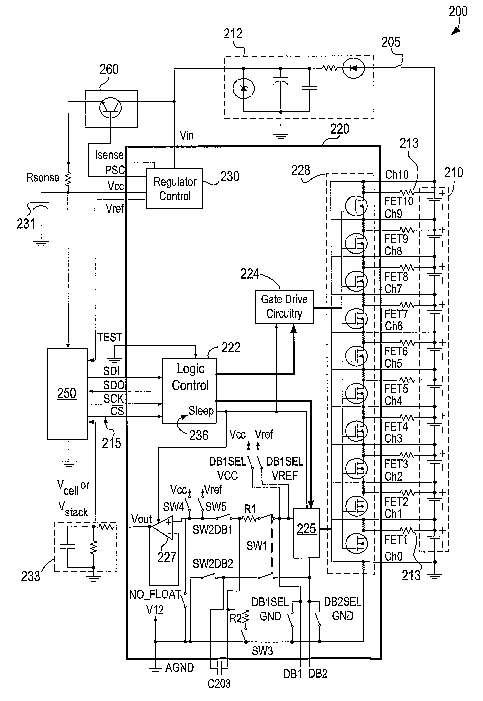
prevalent throughout the workplace and home. Rechargeable batteries may be
used
in numerous devices, from computer products and/or housewares to power tools.
Nickel-cadmium, nickel-metal-hydride battery and/or lithium-ion cells may be
used in
these devices. Since the devices use a plurality of battery cells, the battery
cells may
be ordinarily packaged as battery packs. These battery packs may be coupled
with
the cordless devices so as to secure the pack to the device. The battery pack
may
be removed from the cordless device and charged in a battery charger or
charged in
the cordless device itself, for example.
SUMMARY OF THE INVENTION
[0003] An example embodiment of the present invention is directed to a battery
monitoring device of a battery pack configured for powering a cordless power
tool.
The device may include an integrated circuit connected to a microprocessor of
the
pack that is external to the integrated circuit, and connected to each of N
battery
cells of the pack. The integrated circuit may be configured to take, singly or
sequentially, a sampled reading comprising one of an individual cell voltage
or a total
pack voltage for all cells in the pack. The sampled reading is filtered in the
integrated circuit prior to being read by the microprocessor.
[0004] Another example embodiment of the present invention is directed to a
method of monitoring battery cells of a battery pack that is configured for
powering a
1
CA 02582361 2007-03-29
WO 2006/041751 PCT/US2005/035395
cordless power tool. In the method, a first serial data command may be
received
from a microprocessor of the pack to take a voltage measurement from channels
connected to one or more of the cells. The voltage measurement may be embodied
as a differential voltage value measured across an individual cell or a
differential
voltage value measured across all cells to reflect a total pack voltage. The
voltage
measurement may be stored in a capacitor and filtered so that the capacitor
charges
up to an average of the differential voltage value for a given cell or across
all cells of
the pack. A second serial data command may be received to connect the
capacitor
to a buffer amplifier so that the microprocessor can read the average voltage
value
off the capacitor.
[0005] Another example embodiment of the present invention is directed to an
arrangement in a battery pack for balancing cell voltages during charging of a
plurality of cells of the pack. The arrangement may include a microprocessor
and an
integrated circuit in operative communication with the microprocessor and
connected
to each of the cells. The microprocessor may direct the integrated circuit to
periodically measure, throughout the duration of charging, the cell voltage
across
each cell of the pack and the total pack voltage in a sequential manner. The
integrated circuit communicates the measured individual cell voltage and a
current
average cell voltage for all cells to the microprocessor. The measured total
pack
voltage is automatically divided by the number of cells within the integrated
circuit to
determine the current average cell voltage. The microprocessor controls
balancing
of each of the cell voltages during the charge based on each measured
individual
cell voltage and the determined current average cell voltage.
[0006] Another example embodiment of the present invention is directed to a
method of adaptively balancing cell voltages of a plurality of cells in a
battery pack
during charging of the battery pack. The method includes continuously
monitoring
cell voltages for each cell in the pack in a sequential manner, and detecting
a voltage
differential for one or more cells. The voltage differential may be
represented as the
difference a given measure cell voltage exceeds a current average cell voltage
value
calculated from the continuously monitoring step. Cell voltages may be
balanced
during the charge by discharging those cells having a detected voltage
differential,
2
CA 02582361 2007-03-29
WO 2006/041751 PCT/US2005/035395
until a measured cell voltage for the discharging cell has dropped to equal
the
average cell voltage.
[0007] Another example embodiment of the present invention is directed to a
battery pack configured to monitor voltages of cells therein, the battery pack
operatively attachable to a cordless power tool. The battery pack includes a
microprocessor and an integrated circuit in operative communication with the
microprocessor for monitoring cell voltages of at least N individual cells and
total
pack voltage during discharge of the pack, based on commands received from the
microprocessor. The battery pack includes a motor control semiconductor device
operatively controlled by the microprocessor. As the battery pack is engaged
to a
cordless power tool, and upon an initial actuation of a trigger of the power
tool, the
microprocessor directs the integrated circuit to sequentially measure the
individual
cell voltages of all the cells. The microprocessor may energize the motor
control
semiconductor device to enabie battery current to flow to a motor of the power
tool, if
the determined individual cell voltages are acceptable as compared to a given
voltage threshold.
BRIEF DESCRIPTION OF THE DRAWINGS
[0008] The example embodiments of the present invention will become more fully
understood from the detailed description given herein below and the
accompanying
drawings, wherein like elements are represented by like reference numerals,
which
are given by way of illustration only and thus are not limitative of the
example
embodiments of the present invention.
[0009] FIG. 1 illustrates a block diagram of a arrangement for monitory
battery
parameters in accordance with an example embodiment of the present invention.
[0010] FIG. 2 is a flow diagram illustrating data flow between the
microcontroller
and ASIC of FIG. 1, in accordance with an example embodiment of the present
invention.
[0011] FIG. 3 is a block diagram illustrating components and terminals of an
example battery pack in accordance with an example embodiment of the present
invention.
3
CA 02582361 2007-03-29
WO 2006/041751 PCT/US2005/035395
[0012] FIG. 4 is a block diagram illustrating components and connection
between
an example battery pack and an example battery charger in accordance with an
example embodiment of the present invention.
[0013] FIG. 5 is a block diagram illustrating components and connections
between
an example battery pack and an example power tool in accordance with an
example
embodiment of the present invention.
[0014] FIGS. 6-8 illustrate example cordless power tools configured to be
powered
from the example battery pack in accordance with the present invention.
DETAILED DESCRIPTION OF THE EXAMPLE EMBODIMENTS
[0015] FIG. 1 illustrates a block diagram of an arrangement for monitoring
battery
parameters in accordance with an example embodiment of the present invention.
The battery monitoring arrangement 200 in FIG. 1 may be configured for sensing
certain battery parameters of a battery pack, such as individual cell voltages
and/or
total stack voltage of the pack.
[0016] The battery monitoring arrangement 200 may be part of a removable power
source adapted to power a system of cordless power tools. Example cordless
power
tools may include a circular power saw 10 (FIG. 6), a reciprocating saw 20
(FIG. 7)
and a drill 30 (FIG. 8). The tools 10, 20 and 30 each may include a
conventional DC
motor (not shown) adapted to be powered by a power source having a given
nominal
voltage rating. In the example embodiments, the tools 10, 20 and 30 may be
driven
by a removable power source having a nominal voltage rating of at least 18
volts. It
will become evident to those skilled that the present invention is not limited
to the
particular types of tools shown in the drawings nor to specific voltages
recited as
examples below. In this regard, the teachings of the present invention may be
applicable to virtually any type of cordless power tool and any supply
voltage.
[0017] The removable power source may be embodied as a battery pack 40 having
a housing which includes battery monitoring arrangement 200 therein for
monitoring
baftery parameters. The battery pack may be a rechargeable battery pack 40.
Battery pack 40 may include a plurality of battery cells within its housing
that are
4
CA 02582361 2007-03-29
WO 2006/041751 PCT/US2005/035395
connected in series, and/or a plurality of serially-connected strings of
cells, in which
the strings are in parallel with one another.
[0018] For purposes of describing the example embodiments, battery pack 40 may
be composed of a plurality of cells having a lithium-ion cell chemistry. As
the
example embodiments are directed to a battery monitoring arrangement 200 for
use
in a cordless power tool environment, which requires power sources with much
higher voltage ratings than conventional low voltage devices using Li-ion
battery
technology, (such as laptop computers and cellular phones) the nominal voltage
rating of the battery pack 40 may be at least 18V.
[0019] However, battery pack 40 may be composed of cells of another lithium-
based chemistry, such as lithium metal or lithium polymer, or other chemistry
such
as nickel cadmium (NiCd), nickel metal hydride (NiMH) and lead-acid, for
example,
in terms of the chemistry makeup of individual cells, electrodes and
electrolyte of the
pack 40.
[0020] Referring now to FIG. 1, the arrangement 200 may be part of battery
pack
40 and includes a battery monitoring device 220. Device 220, which in FIG. 1
is
shown as a single integrated circuit (IC) 220, interfaces and/or is in
operative
communication with a pack controller 250 within the housing of battery pack
40, and
a stack 210 of up to N battery cells. The pack controller may be referred to
hereafter
as a digital microprocessor 250. In an example, N may be at least 5 cells,
with
stack 210 being comprised of a number of cells in a range of about 5 to 20
battery
cells. In other examples, the stack 210 may be embodied by a seven (7) cell
configuration, a fourteen (14) cell configuration and/or the illustrative ten
(10) cell
configuration shown in FIG. 1. In each of the previous examples, the battery
pack
40 may be capable of providing an output voltage to its attached cordless
power tool
in a range of about 18-40 volts. In an additional example, the battery pack 40
may
be configured within a range of 7-14 cells to realize a pack voltage between
about 25
to 36 volts. These voltages and cell counts for pack 40 are merely exemplary,
the
present invention is not so limited to the above cell configuration and/or
voltage
ratings.
CA 02582361 2007-03-29
WO 2006/041751 PCT/US2005/035395
[0021] As will be explained hereafter, by using digital communications, such
as
three-wire serial communication, for example, the microprocessor 250 may send
and
receive commands to and from IC 220. As will be explained in further detail
below,
IC 220 may be directed, via one or more serial data commands sent over serial
data
lines 215 by microprocessor 250, to sequentially sample channels corresponding
to
the battery cells of stack 210 and to level shift each of the sampled readings
to a
buffered output at buffer amp 227 to the microprocessor 250 via an A/D pin so
as to
measure the sampled reading. As will be seen below, IC 220 is also capable of
discharging individual or multiple cells through internal balancing
semiconductor
devices, as commanded by the microprocessor 250.
[0022] In FIG. 1, the block diagram of arrangement 200 may represent only a
portion of the internal circuit makeup of the battery pack 40 shown in any of
FIGS. 6-
8. The battery pack 40 may include additional functionality or components such
as
other microprocessors or controllers, a current sensor, a pack temperature
sensor,
pack identification component(s), current limiting device(s), other protection
circuits
such as fuses and/or other internal components for example, which are not
shown
herein for reasons of clarity.
[0023] Although in FIG. 1, IC 220 is shown as a single application specific
integrated circuit (ASIC), the battery monitoring device may be further
embodied in
hardware or software as a digital microcontroller, a microprocessor, an analog
circuit, a digital signal processor or by one or more digital ICs such as
multiple
application specific integrated circuits (ASICs), for exampie.
[0024] The pack controller in FIG. 1 hereafter is described as a digital
microprocessor 250, and may be embodied as a Pentium processor by Intel .
Alternatively, this controller may be configured as an analog circuit, a
digital signal
processor, and/or embodied as one or more digital ICs such as application
specific
integrated circuits (ASICs), etc., for example. In the example embodiments and
as
described hereafter, the microprocessor 250 is external to and not part of IC
220, as
microprocessor 250 resides separately within the housing of the battery pack
40, in
communication with IC 220 via a series of serial data lines 215.
6
CA 02582361 2007-03-29
WO 2006/041751 PCT/US2005/035395
[0025] Each of the example battery cells in stack 210 has a corresponding
selectable channel, Ch1 to Ch10. The channels represent pins of the IC 220.
For
example, ChO is an ASIC pin connected to the negative side of its cell (cell
1) on the
low side or bottom of battery stack 210, CH1 is the pin connected to the
positive side
of cell 1 and the negative side of cell 2, etc. The pins labeled FET1 through
FET 10
represent pins of corresponding semiconductor devices (field effect
transistors FET1
through FET 10) and are connected to the positive sides of cells 1-10. The
function
of FETs 1-10 will be explained in further detail below. IC 220 is operatively
connected to corresponding channels of each cell in the stack 210. Each
channel
thus may be configured to provide a channel input from its corresponding cell
to the
IC 220.
[0026] Arrangement 200 may include a voltage regulator 230 that supplies an
internal control voltage (low voltage Vcc) to the IC 220 and microprocessor
250. For
example, when the trigger switch 205 of an attached power tool is closed, the
stack
210 of battery cells (or a charger) may supply a given input voltage Vin to
the
regulator 230, which, in turn, supplies a stepped down internal control
voltage Vcc to
the IC 220 and microprocessor 250. The Vcc supplied to the IC 220 may be
filtered,
such as by including filtering circuitry 231. A regulator bypass transistor
260 may be
provided to dissipate power, so that power is not dissipated in the regulator
230.
The PSC signal from the voltage regulator 230 controls the base current in
transistor
260 so that VCC remains in a desired stable range, as is known. The voltage
reference (Vref) provided by regulator 230 to microprocessor 250 is a constant
Vref
for the A/D converter (not shown) in the microprocessor 250.
[0027] Accordingly, IC 220 is intended to interface microprocessor 250 and a
stack
210 of up to N battery cells. Using three-wire serial communication, for
example, the
microprocessor 250 may send and receive commands to and from the IC 220. The
IC 220 device is connected to the stack 210 of battery cells and has access to
each
cell voltage. Power for the IC 220 may be supplied from a low voltage Vcc pin
and a
high voltage Vin pin or Vin power terminal. The Vin power terminal may be
separate
from the Ch10 terminal. The Vin power terminal may be filtered, such as by
including filtering circuitry 212 and thus, may be subject to less intense
voltage
7
CA 02582361 2007-03-29
WO 2006/041751 PCT/US2005/035395
fluctuations. IC 220 may also receive external Vcc power on the Vcc pin if the
PSC
pin is left open. By reading the voltage across Rsense, IC 220 can limit the
current
through the bypass transistor 260. Once Vcc is established, the IC 220 creates
a
temperature-stabilized Vref for the A/D converter in the microprocessor 250.
[0028] Data communication may be embodied via serial transmission using a
suitable interface. IC 220 may thus include a logic controller 222 for data
communications between the microprocessor 250 and IC 220. As an example,
logic controller 222 may be embodied as a Serial Peripheral Interface (SPI)
logic
controller.
[0029] In general, a SPI may be used for a synchronous serial communication
between a host processor, such as the microprocessor 250 and peripherals such
as
the logic controller 222 in the IC 220. The SPI typically is configured with
two control
lines, chip select (CS) and clock (SCK) and two data lines, serial data in
(SDI) and
serial data out (SDO). Although only one direction is shown for SDI and SDO
pins,
both the microprocessor 250 and IC 220 have respective SDI and SDO pins. Data
flow thus may be transmitted from the SDO pin of the controller 250 to the SDI
pin of
the IC 220, and/or from SDO pin of the IC 220 to the SDI pin of the controller
250, as
is known. With the CS pin, the corresponding peripheral device is selected.
This pin
is primarily active-low. In an unselected state, the SDO lines are in a high-
impedance state (hi-Z) and therefore inactive. The SCK line is brought to the
device
(IC 220) whether it is selected or not. The SCK signal serves as
synchronization of
the data communication.
[0030] In general SPI operation, a master device (microprocessor 250) decides
with which peripheral device (i.e., IC 220) it wants to communicate. The
master
device provides the clock signal SCK and determines the state of the chip
select
(CS) lines, i.e. it activates the slave (IC 220) it wants to communicate with.
CS and
SCK are therefore outputs. The slave device (such as the IC 220) receives the
SCK
and CS select from as inputs. This means there is one master, while the number
of
slaves is only limited by the number of chip selects. If a SPI device is not
selected,
its data output (SDO) goes into a high-impedance state (hi-Z), so that it does
not
interfere with currently selected devices.
8
CA 02582361 2007-03-29
WO 2006/041751 PCT/US2005/035395
[0031] An SPI device can be a simple shift register up to an independent
subsystem. The length of the shift registers may differ from device to device.
Normally the shift registers may be 8-Bit or integral multiples of it. There
also exist
shift registers with an odd number of bits. For example, two cascaded 9-Bit
EEPROMs can store 18-Bit data.
[0032] Although serial communication between the microprocessor 250 and IC 220
described herein is based on the example SPI logic controller 222, it is
evident to
those of skill in the art that the arrangement could achieve desirable serial
communication between devices using Inter IC (12C) and/or Universal
Asynchronous
Receiver/Transmitter (USART) interfaces and/or chip components in place of the
SPI
logic controller of FIG. 1.
[0033] SPI logic controller 222, in addition to being the interface for
communications between microprocessor 250 and IC 220, is in operative
communication with various additional components of IC 220. For example, SPI
logic controller 222 may output control signals (based on commands received
from
microprocessor 250) to drive gate drive circuitry 224 and/or a switch matrix
225.
The component arrangement that comprises gate drive circuitry 224 is known in
the
art and thus is not described herein for reasons of brevity. In an example,
switch
matrix 225 may be embodied as an analog multiplexer. The function of the
switch
matrix 225 is to select given channel(s) for sampling and acquisition of
battery pack
parameters based on the control signal(s) received from SPI logic controller
222
(which in turn correspond to the given data command received from
microprocessor
250).
[0034] Based on a received command from microprocessor 250, SPI logic
controller 222 may also output control signals to drive the gate drive
circuitry 224, so
as to switch a given semiconductor device (FET) in semiconductor device stack
228
to either ON or OFF. These FETs may be controlled, via SPI logic controller
222
and gate drive circuitry 224, so as to selectively permit discharge of a given
cell (or
not), hence FETs 1 to 10 may be occasionally referred to as "balance FETs".
Each
channel may be connected with a corresponding balance FET in stack 228. The
9
CA 02582361 2007-03-29
WO 2006/041751 PCT/US2005/035395
control and operation of the balance FETs in stack 228 will be explained in
further
detail below.
[0035] As another example, based on a received command from microprocessor
250, SPI logic controller 222 may output control signals directing the switch
matrix
225 to monitor a battery parameter of a given channel, and/or to sequentially
and/or
switch from channel to channel over a given duration (or continuously) to
monitor
certain battery parameters of each the N cells, including total battery stack
voltage
(e.g., total battery pack voltage). Accordingly, and based on the digital data
command received from microprocessor 250, switch matrix 225 may be directed
(via
control signals from SPI logic controller 222) to select channels for
monitoring
various battery parameters, including, but not limited to: cell voltage of a
selected
individual cell, total pack voltage (i.e. total battery stack voltage),
internal or external
voltage references, pack temperatures, and/or monitoring a ground to ground
connection for error correction, etc.
[0036] In general, and based on the command received, the switch matrix 225
selects designated channels to sample the battery parameter of interest.
Although
sample and acquisition processes will be explained in more detail below, in
general,
the sampled reading or parameter of the cell being sampled (in this example a
cell
voltage value) is first stored as an average voltage value onto an external
capacitor,
shown as C203 in FIG. 1. The capacitor 203 is external to IC 220 to allow the
circuit
designer flexibility in sizing the filter frequency. The output of switch
matrix 225
(which is a differential voltage value measured from two channels, one on
either side
of the given cell of interest as shown in FIG.1 or Table 1) is digitally
filtered through
an RC filtering circuit formed by capacitor C203 and internal resistor R1 in
FIG. 1, as
capacitor C203 is being charged.
[0037] The filtering desirably removes high frequency noise (which may be due
to
the discharge of the battery pack, or from the switch matrix 225). Due to
filtering, the
signal being stored as C203 charges up is an average voltage value across the
cell
of interest (e.g., the average of the differential cell voltage taken from the
two
channels bracketing the cell). This may provide a more accurate measurement to
the microprocessor 250's A/D converter, for example.
CA 02582361 2007-03-29
WO 2006/041751 PCT/US2005/035395
[0038] Thus, with filtering provided by the RC filtering circuit (R1 and
C203), C203
charges up to the average voltage across the cell. After a software controlled
delay
to allow C203 to charge, and based on another data command received from
microprocessor 250, the capacitor C203 is disconnected from switch matrix 225
and
connected to buffer amp 227. Buffer amp 227 receives the stored average
voltage
value from C203, an analog voltage signal. Buffer amp 227 is provided so that
capacitor C203 does not bleed off while the microprocessor 250 is taking the
measurement. The Vout sent (via buffer amp 227) to the A/D converter in the
microprocessor 250 is a much cleaner analog signal representation of the
measured
cell voltage, as compared to what would be present without filtering.
[0039] As shown in FIG. 1, the output of the buffer-amp 227, Vout, may be fed
through an optional external filter or conditioning circuit 233 to the A/D
converter
within microprocessor 250 for analog to digital conversion into a digital
voltage value.
No offset correction to the digital voltage value of Vout is required to be
performed in
microprocessor 250 in order to detect (measure) an accurate cell voltage.
Because
C203 is tied to ground via switch SW2DB2, as shown in FIG. 1, the copy of the
average voltage of the selected cell on C203 is now ground referenced and
ready for
reading, as Vout from buffer-amp 227, by the A/D converter in microprocessor
250.
[0040] Thus, various 8-bit commands sent by the microprocessor 250 through the
SDI line may direct the IC 220 to take a measurement and output the analog
measurement value through the Vout pin via a conditioning circuit 233 to the
microprocessor 250 digital conversion and detection (measurement). This
enables
the microprocessor 250 to read any individual cell voltage within the stack
210
without having to perform two or more single-ended measurements and/or a
digital
subtraction or offset correction to determine (measure) the cell voltage.
[0041] Accordingly, to sample a battery pack parameter such as an individual
cell
voltage, and referring to FIG. 1, a command is sent from the microprocessor
250 to
the SPI logic controller 222. SPI logic controller 222 in turn sends control
signals to
close switch matrix 225 and select the given channel to DB1 and DB2 pins of
IC220,
and to align switch positions (SHUNT of OPEN) for sampling, e.g., switches
SW2DB1, SW2DB2, DB1 SELGND and DB1 SELGND all have logic low states (= 0)
11
CA 02582361 2007-03-29
WO 2006/041751 PCT/US2005/035395
or OPEN, and switch SW1 =1 (SHUNT) to take the sampled reading as capacitor
C203 is charged through resistor R1.
[0042] After a software controlled delay (which may be a few milliseconds),
the SPI
logic controller 222 may receive another command from microprocessor 250 to
open
switch matrix 225, open switch SW1 and shut each of switches SW2DB1, SW2DB2,
DB1 SELGND and DB1 SELGND (logic high = 1). This connects C203 to buffer amp
227 for output as Vout, e.g., an analog average voltage value of the cell, to
the
microprocessor 250
[0043] Other commands may enable and/or disable a given balance FET on a
given channel where the intent is to drain a specific current which is set by
external
resistors 213. As will be shown below in further detail, a command may be sent
by
microprocessor 250 to direct the IC 220 to read the total stack voltage with
an
automatic divide by ten on the output of switch matrix 225.
[0044] Table 1 provides an example list of 8-bit commands that may be
transmitted
by microprocessor 250 over the SDI line to the IC 220. Across the top row of
Table
1, there is shown the 8-bit command (Data Line), what is selected to the DB1
and
DB2 pins of the IC 220, the switch positions for switches SW1, SW2 (DB1 and
DB2),
SW3, SW4 and SW5, and the action of a given FET in FET stack 228.
Table 1 - Example Command Structure
Data Line DB1 DB2 Sl S2 S3 S4 S5 FET Action
0000 0000 Gnd Gnd Open Shunt Open Open Open No Change
0000 0001 Chl ChO Shunt Open Open Open Open No Change
0000 0010 Ch2 Chl Shunt Open Open Open Open No Change
0000 0011 Ch3 Ch2 Shunt Open Open Open Open No Change
0000 0100 Ch4 Ch3 Shunt Open Open Open Open No Change
0000 0101 Ch5 Ch4 Shunt Open Open Open Open No Change
0000 0110 Ch6 Ch5 Shunt Open Open Open Open No Change
0000 0111 Ch7 Ch6 Shunt Open Open Open Open No Change
0000 1000 Ch8 Ch7 Shunt Open Open Open Open No Change
0000 1001 Ch9 Ch8 Shunt Open Open Open Open No Change
0000 1010 Ch10 Ch9 Shunt Open Open Open Open No Change
0000 1011 Vcc Gnd Open Open Open Open Open No Change
0000 1100 Vref Gnd Open Open Open Open Open No Change
0000 1101 Gnd Gnd Open Open Open Shunt Open No Change
0000 1110 Gnd Gnd Open Open Open Open Shunt No Change
0000 1111 ChlO ChO Shunt Shunt Shunt Open Open No Change
0010 0001 Chl ChO Shunt Open Open Open Open FET 1 On
0010 0010 Ch2 Chl Shunt Open Open Open Open FET 2 On
12
CA 02582361 2007-03-29
WO 2006/041751 PCT/US2005/035395
0010 0011 Ch3 Ch2 Shunt Open Open Open Open FET 3 On
0010 0100 Ch4 Ch3 Shunt Open Open Open Open FET 4 On
0010 0101 Ch5 Ch4 Shunt Open Open Open Open FET 5 On
0010 0110 Ch6 Ch5 Shunt Open Open Open Open FET 6 On
0010 0111 Ch7 Ch6 Shunt Open Open Open Open FET 7 On
0010 1000 Ch8 Ch7 Shunt Open Open Open Open FET 8 On
0010 1001 Ch9 Ch8 Shunt Open Open Open Open FET 9 On
0010 1010 Ch10 Ch9 Shunt Open Open Open Open FET 10 On
0010 1111 Ch10 ChO Shunt Shunt Shunt Open Open All FETs On
0011 0001 Chl ChO Shunt Open Open Open Open FET 1 Off
0011 0010 Ch2 Chl Shunt Open Open Open Open FET 2 Off
0011 0011 Ch3 Ch2 Shunt Open Open Open Open FET 3 Off
0011 0100 Ch4 Ch3 Shunt Open Open Open Open FET 4 Off
0011 0101 Ch5 Ch4 Shunt Open Open Open Open FET 5 Off
0011 0110 Ch6 Ch5 Shunt Open Open Open Open FET 6 Off
0011 0111 Ch7 Ch6 Shunt Open Open Open Open FET 7 Off
0011 1000 Ch8 Ch7 Shunt Open Open Open Open FET 8 Off
0011 1001 Ch9 Ch8 Shunt Open Open Open Open FET 9 Off
0011 1010 Ch10 Ch9 Shunt Open Open Open Open FET 10 Off
0011 1011 "Wake up" Shunt Shunt Open Open Open All FETs Off
0011 1110 Sleep Mode Open Open Open Open Open All FETs Off
0011 1111 Ch10 ChO Shunt Shunt Shunt Open Open All FETs Off
[0045] As shown in FIG. 1, there is provided an auxiliary circuit (consisting
of
switches DB1 SELVcc, DB1 SELVref, DB1 SELGND and DB2SELGND) for an
external device that is connectable to pins DB1 and DB2. In an example, the
external device may be a high voltage differential amplifier, which could be
added to
replace the switch-capacitor arrangement of switches SW 1-SW5 and C203 (e.g.,
switch-capacitor arrangement) in IC 220, or to provide a back-up battery
monitoring
means if the switch-capacitor arrangement fails. Accordingly, the external
differential
amplifier would be connected to the output of the switch matrix 225 to provide
differential voltage measurements from the directly to the A/D converter of
the micro
250?, clarify].
[0046] By using command "0000 1101" and reading the voltage on Vout, the
microprocessor 250 can determine whether or not the external amplifier is
connected
to DB1 and DB2. In an example, if an external device is used, the voltage
reading
will be ground potential (GND). If the IC220 is used, then the voltage reading
will be
volts. If the external amplifier is used, the command "0000 0000" is not used
for
acquisition.
Individual cell voltage measurements
13
CA 02582361 2007-03-29
WO 2006/041751 PCT/US2005/035395
[0047] Referring to Table 1, and in an example, assume a command "0000 0111
is sent from the microprocessor 250 to the IC 220, which is a command for
measuring the cell voltage of cell 6 between channels Ch6 and Ch7. As can be
seen from Table 1, this command made no changes to the status of any of the
balance FETs in stack 228. The command is processed by SPI logic controller
222
and returned back to the microprocessor 250 during the next byte transfer on
the
SDO line for verification. This is because immediately following the original
command, the microprocessor 250 continues to toggle the SCK line, while the
logic
controller 222 sends the original command back for verification.
[0048] Once read, the SPI logic controller 222 controls the switch matrix 225
to
select Ch7 to the DB1 pin and to select Ch6 to the DB2 pin, so as to sample a
differential voltage representative of the cell voltage at cell 6. At the same
time, SW1
closes to start charging capacitor C203 across pins DB1 and DB2, via the RC
network formed by R1 and C203. Accordingly, due to the filtering of the RC
network,
capacitor C203 stores an average of the differential voltage for cell 6,
rather than the
immediate differential voltage for cell 6 which could fluctuate wildly as
charge/discharge currents change.
[0049] After a software controlled delay, the microprocessor sends a second
command 0000 0000. As shown in Table 1, this command opens switch matrix 225
and switch SW1 and shuts each of switches SW2DB1, SW2DB2, DBISELGND and
DB1 SELGND (logic high = 1). This connects C203 to buffer amp 227 to feed Vout
to
the microprocessor 250's A/D converter. The remaining cells of stack 210 can
be
read the same way.
Total stack voltage measurement
[0050] A command may be used by microprocessor to read total stack voltage. To
measure total stack voltage, microprocessor 250 sends the command "0000 1111"
to
the IC 220, which is a command for measuring the total stack voltage between
CHO
and Ch10. The command is processed by SPI logic controller 222 and returned
back to the microprocessor 250 during the next byte transfer on the SDO line
for
verification. As shown in Table 1 and with reference to FIG. 1, the SPI logic
controller 222 controls the switch matrix 225 to select Ch10 to the DB1 pin
and to
14
CA 02582361 2007-03-29
WO 2006/041751 PCT/US2005/035395
select ChO to the DB2 pin, so as to sample a differential voltage representing
the
total stack voltage of the battery pack. At the same time, switches SW1, SW2
and
SW3 close to start charging capacitor C203 across pins DB1 and DB2, through a
voltage divider circuit formed by R1 and R2 that charges capacitor to the
average
voltage of the stack at a 10:1 ratio. The 10:1 ratio is thus set by the values
of R1
and R2.
[0051] The voltage value being stored on capacitor C203 is filtered through
the RC
network formed by R1 and C203 to obtain an average voltage value of the total
stack
voltage. After a software controlled delay, the microprocessor 250 may send
command 0000 0000 to connect C203 to buffer amp 227 to feed Vout to the
microprocessor 250's A/D converter. However, since switch SW2 is shut during
sample and acquisition of total stack voltage, the microprocessor 250's A/D
can
continuously measure total stack voltage.
[0052] The switch matrix 225 can change to any channel from any other channel
without shorting the cell voltages, which ordinarily may cause a shoot-through
condition. Shoot-through is a condition that normally occurs during a
transition of a
switch from one connection to another. If a switch were to make contact with
one
branch of a circuit before breaking contact with a second branch, current
could flow
from the first branch to the second branch. This is an undesirable condition
and thus
most switches are designed with a "break before make" contact system. The
output
of the switch matrix 225 is thus filtered by the RC circuit before entering
the buffer-
amp 227.
[0053] In FIG. 1, the CS pin is the Chip Select. When pulled low, the SPI
logic
controller 222 will function normally. When pulled high, the SPI logic
controller 222
send and receive logic is reset. This function is useful for packet/byte
synchronization to keep the IC 220 bit counter synchronous with the master
clock.
The SDO pin may be set to tri-state during this reset, as is known.
[0054] IC 220 may include a SLEEP pin, shown generally at 236. Referring to
FIG.
1 and Table 1, a SLEEP command 0011 1110, when given, will cause IC 220 to be
switched into a low-power sleep mode. Thus, as the SLEEP pin 236 is pulled
low,
the IC 220 is switched into a low-power sleep mode. All FET's in stack 228 are
CA 02582361 2007-03-29
WO 2006/041751 PCT/US2005/035395
disabled and the Vout is disabled and switched to a high Z state. SPI logic of
logic
controller 222 is also disabled during sleep mode and the SDO pin is set to
tri-state.
[0055] Also in table 1, a specific "wakeup" command 0011 1011 is provided to
bring
IC220 out of the sleep mode. When coming out of sleep mode, the SPI logic is
reset regardless of the status of the CS pin. The balance FETs in stack 228
are also
reset to the "OFF" state upon awakening.
[0056] FIG. 2 is a flow diagram illustrating general data flow between the
microprocessor 250 and IC 220 of FIG. 1, in accordance with an example
embodiment of the present invention. In general, microprocessor 250 sends a
command (S21 0) to IC 220 by clocking the SCK pin and sending the 8-bit data
command on its SDO pin, to be received by the SDI pin of the IC 220. The IC
220
receives the command (S220) and processes the analog output. The
microprocessor 250 then clocks the SCK pin (S230) to receive the original
command
back from the IC 220 over the microprocessor 250' s SDI pin, for verification
to the
microprocessor 250 that the IC 220 understood and implemented the correct
command.
[0057] If the responding command is different from the original command, the
microprocessor 250's A/D reading (detected or measured value received from IC
220) is discarded and the original command can be resent. This two byte
transfer
may be considered excessive for use in electrically quiet, noise-free
environments.
In that case, a standard SPI protocol may be used where hand-shaking is done
bit-
by-bit instead of byte-by-byte. Hand-shaking may be defined as the act of
receiving
a signal and transmitting it back to the originator for verification.
[0058] FIG. 3 is a block diagram illustrating components and terminals of an
example battery pack in accordance with an example embodiment of the present
invention; and FIG. 4 is a block diagram illustrating components and
connection
between an example battery pack and an example battery charger in accordance
with an example embodiment of the present invention.
[0059] As an implementation example, the arrangement 200 of FIG. 1 is
described
in the context of a battery pack 300 as shown in FIGS. 3 and 4. The block
diagram
of battery pack 300 only shows the salient features of arrangement 200 for
purposes
16
CA 02582361 2007-03-29
WO 2006/041751 PCT/US2005/035395
of clarity. It may be understood that the battery pack 300 could have
additional
sense components in operative communication with microprocessor 250, for
example, such as a current sensor, temperature sensor, pack ID device, current
limiting device, etc. Hereafter, example features and functions of the IC 220
during
an example charge and discharge cycle are described.
[0060] Referring to FIG. 3, battery pack 300 is shown in an inactive state,
not
connected to any electrical device. In FIG. 3, four terminals (terminals 1-4)
are
shown. However, the example embodiments should not be limited to this terminal
configuration, as greater or fewer terminals could be included, depending on
the
desired information to be passed between the battery pack 300 and another
connectable electrical device such as a power tool or charger.
[0061] The cells of battery stack 210 may be completely dead (0 Volts) in this
example, with the battery pack 300 sitting idle on a shelf. As shown in FIG.
3, the
regulator 230 is not powered, so IC 220 and microprocessor 250 are idle and
nothing
is live. By placing the battery pack 300 into the charger 400 (FIG. 4), the
following
events occur:
(i) The charger 400 supplies a source voltage (here shown as an example
15 Volts) to the bypass transistor 260 and the Vin pin, which in turn
coLitrols the regulator 230 through the PSC pin.
(ii) The regulator 230, in turn, supplies an example 5 Volts (Vcc) to the
microprocessor 250 and IC 220 (low voltage Vce pins).
(iii) The microprocessor 250 resets and begins initializing its own program
parameters. The resets and initialization routines may be similar to that
done by a microprocessor of a PC or laptop upon start-up, for example,
and are not explained in detail as these procedures are not a focus of
the invention.
(iv) After initialization, the microprocessor 250 communicates with the
charger 400 (such as with the charge control 420) via serial
communications (not shown for clarity).
17
CA 02582361 2007-03-29
WO 2006/041751 PCT/US2005/035395
(v) Microprocessor 250 maintains motor control FET 240 OFF, since
microprocessor 250 has determined that battery pack 300 is connected
to a charger 400 and not a power tool.
Charge Cycle
[0062] Referring to FIG. 4, before charging can commence, the A/D readings
(values of cell voltages) should be known. The first cell (cell between
channels ChO
and Ch1 in FIG. 1) may be chosen by microprocessor 250 sending command 0000
0001 to IC 220. The data may be clocked out to IC 220, and after a brief
waiting
period, a return byte may be clocked back in by the microprocessor 250. The
returned byte should match the original command if communication was
effective.
[0063] While the microprocessor 250 is verifying the returned command, IC220
is
putting the first cell's voltage on its DB1 and DB2 pins. The external
capacitor C203
is charged through the internal resistor R1. After a software controlled
delay, the
microprocessor 250 sends a second command 0000 0000 to connect capacitor
C203 to buffer amplifier 227 to feed Vout to the microprocessor 250's A/D
converter.
The remaining cells in stack 210 can be read the same way. With the cell
voltages
known, the microprocessor 250 in the battery pack 300 may command the charger
400 to begin charging.
Dynamic Cell Balancing durinqCharge
[0064] The cells of stack 210 increase in voltage as they are charged. Not all
of the
cells have the same capacity, so some of the cell voltages are higher than
others.
To head off potential overcharge events, the cells may be monitored
sequentially
and continuously as often as needed by microprocessor 250, in an effort to
detect a
voltage differential For example, IC 220 may be directed by microprocessor 250
to
scan the entire cell stack 210 in about 10 milliseconds, but due to the slow
nature of
charge, longer cycling times could be employed. In any event, the measuring,
evaluating of cell voltages against a threshold and balancing of cells
voltages may
be repeated throughout the charge as necessary so as to maintain all cell
voltages
substantially balanced during the charge.
[0065] Each cell may thus be sampled by microprocessor 250 via data commands
sent to IC 220, with the detected or measured value stored in an associated
internal
18
CA 02582361 2007-03-29
WO 2006/041751 PCT/US2005/035395
or external memory of microprocessor 250. When a complete scan is taken, for
example, the total stack voltage may be taken as an eleventh measurement. This
value is scaled or automatically divided by 10 in IC 220 via the voltage
divider circuit
(R1 and R2), such that capacitor C203 charges to an average cell voltage for
all the
cells. If all the individual cell voltage measurements are added, the
measurements
should add up to the average cell voltage times ten. This procedure may be
used as
an error check on system integrity, for example.
[0066] Moreover, the average cell voltage may also be used as a running,
relative
reference value, or threshold. This threshold may be to determine which
individual
cells have smaller capacity during the charge and thus are charging faster
than the
rest. Such smaller capacity cells could pose a problem if left unattended
during
charge. As an example, and for lithium-ion cells, an overcharge condition is
highly
undesirable for the cell. In the example of FIG. 1, if nine of the cells are
at 4 volts,
and the tenth cell is at 4.2 volts (max voltage), the total stack 210 voltage
reading is
only 40.2 volts. This does not mean it is permissible to continue charging,
since the
cell at 4.2 volts would be damaged if charging were continued. Accordingly, it
is
desirable to provide active cell balancing during the charge, so that the
voltage of the
tenth cell (or sixth cell, fourth cell, etc., for example) never gets any
higher in voltage
than the average cell voltage value for all cells. This way, all cells in
stack 210 reach
the peak voitage together.
[0067] The microprocessor 250 may thus direct IC 220 to continuously monitor
each of the cells in a sequential manner, taking individual and total stack
voltage
measurements so as to detect any voltage differential between the detected
individual cell voltage and the average cell voltage for all cells, which is
determined
from the automatic division of the total stack voltage by 10. In a particular
example,
and referring to FIG. 1, the detected voltage of cell number 4 (between Ch3
and
Ch4) is slightly higher than the reference value, e.g., the determined average
cell
voltage for all the cells in stack 210. To speed the balancing of the cells,
the
microprocessor 250 is able to dynamically detect this voltage differential
based on a
digital comparison between the stored A/D value for the cell (e.g., the
detected cell
voltage value for cell 4) from command 0010 0100 in Table 1, and the stored
19
CA 02582361 2007-03-29
WO 2006/041751 PCT/US2005/035395
average cell voltage A/D value measured by IC 220 when sampling the total
stack
voltage, as directed by command 0000 1111).
[0068] Arrangement 200 may thus be configured to cycle through all cell
voltage
measurements in about 10 milliseconds, and then may compare the measured
individual cell A/D values to the measured average cell voltage A/D value to
dynamically determine "unbalanced" cells. If the microprocessor 250 determines
that cell 4 is slightly higher in voltage than the average cell voltage of the
cells in
stack 210, microprocessor 250 issues a data command 0010 0100 to the IC 220.
This command tells the IC 220 to turn the balance FET 4 in semiconductor
device
stack 228 to the ON-state. The cells are all being charged at the same rate
except
for cell 4, whose charge rate is lowered by the discharge rate with FET 4 ON.
This
allows the other cells to "catch up" to cell 4, as the individual cell voltage
of cell 4
drops so as to meet the average cell voltage of the stack 210.
[0069] So far, determining whether to discharge particular cells during charge
in an
effort to obtain balanced cell voltages across the pack 300 has be described
using
the average cell voltage of all cells is stack 210 as a baseline or reference
value,
(e.g., as a threshold). However, discharging the cell having a maximum
differential
voltage from the average cell voltage of the stack 210 is only one example
threshold.
In an alternative, after IC 200 performs each cycle of individual cell voltage
measurements under the direction of the data commands from microprocessor 250,
microprocessor 250 can issue a command to IC 220 to discharge the highest
voltage
cell as evident from the individual cell voltage measurements. In another
alternative, based on the voltage measurements received in a given (or each)
cycle
of measurements, microprocessor 250 can issue a command to IC 220 to discharge
multiple cells, such as the X highest voltage cell(s), as evident from the
individual cell
voltage measurements. In a further alternative, microprocessor 250 may issue a
special command to IC 220 to discharge those cell(s) whose cell voltage
measurement exceeds a given voltage threshold, such as Y muitiplied by a
minimum
voltage for the cell that may be set in advance (Y being an integer ? 1).
These
methodologies represent other example types of threshold criteria for
discharging
CA 02582361 2007-03-29
WO 2006/041751 PCT/US2005/035395
one or more cells in the pack 300 during a charge, in an effort to balance
cell
voltages evenly during and upon completion of the charge.
Determining total stack voltage of Cell Stack durinc1Charqe
[0070] As discussed above, and in addition to monitoring the individual cell
voltages, the IC 220 may be commanded to measure the total stack voltage of
stack
210 with command 0000 1111. As described earlier, the total stack 210 voltage
may
be automatically divided by 10 inside IC 220, which provides an average cell
voltage
value for cells of the stack 210. The individual A/D readings received by the
microprocessor 250 should add up to ten times the stack A/D measurement (i.e.,
the
average cell voltage used by the microprocessor 250 to determine voltage
differential for each of the cells in stack 210 in a continuous manner) sent
as V ut to
the A/D pin of the microprocessor 250. This function may be done as a back up
to
the cell checking to prevent overcharge.
Additional Example-Cell Balancing
[0071] As time during the charge elapses, one or more additional cells could
begin
to have a slightly higher voltage than the average cell voltage for the cells.
These
additional cell(s) may be discharged by the IC 220 concurrently with cell 4,
after
being commanded to do so by the microprocessor 250. This may be performed as
was described for cell 4 above. When scanning the cells that are being
discharged,
(cell 4 for example), the most accurate measurement for cell 4 can be made
with
data command 0011 0100. This directs the IC 220 to output the cell 4 voltage,
but it
also turns off (unlatches) the balance FET for that cell (FET4). With no
current being
discharged, the voltage of cell 4 is a reasonably sound indicator of its state-
of-
charge. When finished reading the channel, the balance FET could be turned
back
on (if deemed necessary) with command 0010 0100.
[0072] Later in the charge, cell 4 voltage has dropped back to the average
cell
voltage of the stack 210. The microprocessor 250 determines this as a trigger
to
stop discharging cell 4. The same command 0011 0100 may be sent to IC 220 to
measure the cell voltage of cell 4 and un-latch the balance FET 4. Now cell 4
can
receive the full charge current that is being received by the remaining cells.
Terminating Charge
21
CA 02582361 2007-03-29
WO 2006/041751 PCT/US2005/035395
[0073] Eventually, the cells in stack 210 all reach a voltage where it is
desirable to
terminate the charge current. The microprocessor 250 can make this decision in
various ways, which are not discussed here, as such termination strategies are
outside the scope of the invention. Microprocessor 250 may communicate with
the
charger 400 (i.e., by serial data communications) so that the charge current
is
suspended. In this example, each cell, when fully charged, may have roughly
4.2
volts of charge; thus the voltage at Ch10 is about 42 volts with respect to
ground.
The Vin pin and regulator 230 are still supplied with the charger 400's 15
volts.
[0074] The pack 300 is removed from the charger 400, and may be placed back in
a tool-box (or other storage area) to sit for a while. The battery cells in
stack 210 still
exert their voltage on the IC 220 pins, but because the Vcc pin is not powered
and
Vin is at zero volts, the IC 220 is shut-down and there is only minimal
leakage
current drain on the cells.
Discharge Cycle - Battery pack operation with power tool
[0075] FIG. 5 is a block diagram illustrating components and connections
between
an example battery pack and an example power tool in accordance with an
example
embodiment of the present invention.
[0076] In an example, such as when a work day begins, the battery pack 300 may
be placed in a tool 500 as shown in FIG. 5. As soon as the tool trigger switch
510 is
actuated, the cell stack 210 voltage of the pack 300 may be applied to the
regulator
230 and Vin pin of the IC 220. After an initialization period, the
microprocessor 250
realizes that it is in a tool (instead of a charger) and checks the cell
voltages. If all
measurements are acceptable, motor control FET 240 is turned on to permit
current
to tool motor 520. For example, measurements may be acceptable if all cell
voltages
are above a given voltage level or voltage threshold, such as a given cut-off
voltage
below which the cell is in an under-voltage condition.
[0077] As during charging, the microprocessor 250 monitors cell voltages
during
discharge of the stack 210. If the trigger switch 510 is released, the voltage
at Vin
and the regulated voltage (5V) supplied to the microprocessor 250 and IC 220
fade
away to ground. With no power supply, the microprocessor 250 shuts down and
the
Motor Control FET 240 is turned off.
22
CA 02582361 2007-03-29
WO 2006/041751 PCT/US2005/035395
[0078] When the trigger switch 510 is pulled again, the IC 220 is powered up
and
the tool motor 520 operation continues. The tool motor 520 will be enabled as
long
as the trigger switch 510 is pulled and the cell voltages are greater than a
given
voltage level or voltage threshold. Once a cell in stack 210 reaches a low
voltage
threshold such as a cut-off voltage, for example, the microprocessor 250 can
command the Motor Control FET 240 to turn off. This action saves the cells of
stack
210 from being over-discharged and prolongs cell life.
[0079] If the trigger switch 510 is left on (in certain cases some users may
tape the
trigger on), the microprocessor 250 will continue to direct commands to IC 220
so as
to continuously monitor cell voltages, but maintains the Motor Control FET 240
in the
off state. Once the total stack voltage has dropped below an example
threshold, in
this example, this may be 25 voits (because of a small discharge current
needed to
power the battery circuit), the microprocessor 250 can tell the IC 220 to go
into sleep
mode via the SLEEP pin 236. This action may substantially reduce power
consumption inside the battery pack 300. The IC 220 will stay in this mode
until the
microprocessor 250 is reset. The battery pack 300 may be eventually removed
from
the tool 500 and placed back on the shelf in a discharged state.
[0080] The above example charge/discharge cycle illustrates how the IC 220 may
operate with the microprocessor 250 to prolong cell life. Over-charge
protection,
over-discharge protection and the ability to perform adaptive cell-balancing
within a
battery pack during a charge may all be accomplished in a battery pack having
an
arrangement 200 that includes the IC 220 and microprocessor 250, for example.
[0081] The example embodiments of the present invention being thus described,
it
will be obvious that the same may be varied in many ways. Such variations are
not
to be regarded as departure from the spirit and scope of the example
embodiments
of the present invention, and all such modifications as would be obvious to
one
skilled in the art are intended to be included within the scope of the
following claims.
23