Note: Descriptions are shown in the official language in which they were submitted.
CA 02583357 2007-04-05
WO 2006/039790
PCT/CA2005/001547
CONTROL APPARATUS AND METHOD FOR USE WITH
DIGITALLY CONTROLLED LIGHT SOURCES
FIELD OF TEE INVENTION
The present invention pertains to the field of lighting and in particular to a
method and
µ.
apparatus for controlling the amount of light emitted by one or more digitally
controlled
light sources.
BACKGROUND
Advances in the development and improvements of the luminous flux of light-
emitting
diodes (LEDs) such as solid state and organic light-emitting diodes have made
these
devices suitable for use. in general illumination applications, including
architectural,
entertainment, and roadway lighting, for example. As such, light-emitting
diodes are
becoming increasingly competitive with light sources such as incandescent,
fluorescent,
and high-intensity discharge lamps.
Light-emitting diodes offer a number of advantages and are generally chosen
for their
ruggedness, long lifetime, high efficiency, low voltage requirements, and the
possibility
to control the colour and intensity of the emitted light independently. They
provide
improvement over delicate gas discharge lamp, incandescent, and fluorescent
lighting
systems. Solid state and improvingly organic light-emitting diodes have the
capability
to create the same lighting impressions of other lighting technologies and can
greatly
outweigh the drawbacks associated therewith.
Unlike for classical incandescent light sources, the intensity and colour of
light emitted
by LEDs can be independently controlled. Provided that parameters, for example
die
temperature, which can affect the spectral distribution of light emitted by
the device
remain constant, the total emitted light can be controlled without
substantially changing
the colour impression. Light emission in an LED only occurs when the current
through
the device exceeds a certain threshold and from there on the current can be
safely
increased up to a specific maximum value. Controlling a stable constant light
output
therefore requires precisely controlling the direct current through an LED.
However,
certain applications only require controlling the average light output over
time.
1
CA 02583357 2007-04-05
WO 2006/039790
PCT/CA2005/001547
Consequently, rapid repetitive switching between no light emission and full
light .
emission such as for example by the use of pulse width modulation (PWM) or
pulse
code modulation_may -be-sufficientto achieve a desired lighting effect.
While PWM is a useful technique for dimming LEDs, it has to meet a number of
special
requirements in order to create apparent lighting effects that will be
pleasantly perceived
by humans. The need for perceptually smooth dimming, particularly with square
law
equalization to compensate for the non-linear brightness response of the human
visual
system, generally requires controlling the light output with 12 to 14 bit
resolution
whereas standard mainstream hardware PWM circuits only support ten bit
resolution.
Moreover, due to the intensity undergoing 100% modulation, the PWM frequency
typically must be higher than about 300 Hz in order to avoid perceptible
flickering of the
light produced. In addition, because the components of LEDs can transport and
store
heat at different rates, higher PWM frequencies can reduce the effects of
stress caused
by thermal cycling of the device and in typical LED packages detrimental
effects of
temperature fluctuations can become negligible for PWM frequencies beyond
about 103
to 10411z,
Brightness control of LEDs has been addressed in a number of United States
patents, for
example U.S. Patent No. 3,787,752 which describes intensity control for a
light emitting
diode display. The invention describes how a series of power pulses can be
used to
effectively control LEDs that are unmatched in their lighting characteristics
for low
electric currents but matched for electric currents near their optimal
operating
conditions. This document however, does not describe how the duty factors of
the
power pulses can be reproducibly and discretely set and is also only defined
as it would
be applied to displays.
U.S. Patent No. 4,090,189 discloses another brightness control circuit for LED
displays.
The invention describes a PWM method for controlling LEDs over a relatively
wide =
range of brightness levels also extending stable operation into the lower
brightness
region. This disclosure also does not describe how the duty factors of the
power pulses
can be reproducibly and discretely set to control brightness of the LEDs at a
desired
resolution.
2
CA 02583357 2007-04-05
WO 2006/039790
PCT/CA2005/001547
United States Patent No. 6,833,691 discloses a system and method for providing
digital
pulse width modulation. The invention describes a pulse width modulation
system for
use in a switching power supply circuit that provides high-resolution pulse
width
modulated signals. The system is configured to receive a control signal
comprising a
(m+n)-bit binary word and to provide a pulse width modulated signal with a
predetermined average duty cycle having a resolution of substantially 2(').
The pulse
width modulation system includes a timing circuit for providing 2" timing
signals, a
dithering circuit, and a signal generator. Upon receiving the control signal,
the dithering
circuit is configured to provide a modified control signal, which comprises a
series of up
to 2" m-bit binary words. The signal generator is configured to receive the
timing
signals and the modified control signal and to provide the pulse width
modulated signal
having a duty cycle, which, when averaged over 2" timing cycles, is
approximately equal
to the predetermined average duty cycle. The pulse width modulated signal is
used by a
switching power supply circuit to control at least one power switching device.
In
particular, this invention uses a complicated signal generating circuit with
adders,
delays, multiplexers, memory, and latch modules. In addition, in its preferred
embodiment, (m+n)-bit control words are mapped into a sequence of m-bit PWM
duty
. factors in a way that creates artefacts when the (m+n)-bit word assumes its
maximum
value of 2m+"-1.
Therefore, there is a need for an improved and simplified control apparatus
and method
for use with digitally controlled light sources that is both robust against
noisy signals
and can effectively enhance the resolution level of control of digitally
controlled light
sources.
This background information is provided to reveal information believed by the
applicant
to be of possible relevance to the present invention. No admission is
necessarily
intended, nor should be construed, that any of the preceding information
constitutes
prior art against the present invention.
SUMMARY OF THE INVENTION
An object of the present invention is to provide a control apparatus and
method for use
with digitally controlled light sources. In accordance with an aspect of the
present
invention, there is provided an apparatus for control of a huninaire including
one or
3
CA 02583357 2007-04-05
WO 2006/039790
PCT/CA2005/001547
more light-emitting elements in one or more colours, each of the one or more
light-
emitting elements supplied with electrical current to produce light, said
apparatus
comprising: means to adjust the electrical current to the one or more light-
emitting
elements using pulse width modulation or pulse code modulation, each of said
pulse
width modulation and pulse code modulation having a pulse cycle; and means to
modulate a pulse width for each pulse cycle, thereby increasing control
resolution of the
one or more light-emitting elements.
In accordance with another aspect of the present invention there is provided
an extended
pulse width modulation method for transforming a (N+M)-bit signal into a
stream of 2m
words of N-bit width for a total of 2m pulse cycles, the method comprising the
steps of:
receiving the (N+M)-bit signal; splitting the (N-FM)-bit signal into an N-bit
portion and
an M-bit portion; interpreting the N-bit portion as a binary coded number n;
interpreting
the M-bit portion as a binary coded number m; encoding (n+1) in a form of a
binary N-
bit word and feeding the word for m pulse cycles into the stream; and encoding
n in a
form of a binary N-bit word for (2m¨ m) pulse cycles and feed the word into
the stream;
. thereby forming the stream of 2m words of N-bit width for a total 012M
pulse cycles.
In accordance with another aspect of the invention, there is provided an
extended pulse
width modulation apparatus for transforming a (N+M)-bit signal into a stream
of 2m
words of N-bit width for a total of 2m pulse cycles, the apparatus comprising:
means for
receiving the (N+M)-bit signal; means for splitting the (N+M)-bit signal into
an N-bit
portion and an M-bit portion; means for interpreting the N-bit portion as a
binary coded
number n; means for interpreting the M-bit portion as a binary coded number m;
means
for encoding (n+1) in a form of a binary N-bit word and feeding the word for m
pulse
cycles into the stream; and means for encoding n in a form of a binary N-bit
word for
(2m ¨ m) pulse cycles and feed the word into the stream; thereby forming the
stream of
2m words of N-bit width for a total of 2m pulse cycles.
BRIEF DESCRIPTION OF THE FIGURES
Figure 1 illustrates the relationship between temporal frequency and contrast
sensitivity
of the human visual system.
4
CA 02583357 2007-04-05
WO 2006/039790
PCT/CA2005/001547
Figure 2 illustrates a block diagram of the control apparatus for a single or
multi-channel
lighting apparatus according to one embodiment of the present invention.
Figure 3 illustrates a block diagram of a luminaire that can be controlled
using the
control apparatus according to the present invention.
Figure 4 illustrates a block diagram of another luminaire that can be
controlled using the
control apparatus according to the present invention.
Figure 5 illustrates a schematic circuit diagram of an embodiment of the
present
invention.
Figure 6 illustrates a schematic circuit diagram of another embodiment of the
present
invention.
=
Figure 7 illustrates a schematic circuit diagram of another embodiment of the
present
invention.
Figure 8 illustrates a flow diagram for a micro controller main program for
controlling
the light sources using PWM, according to one embodiment of the present
invention.
Figure 9 illustrates a flow diagram for a subroutine for the main program as
illustrated in
Figure 8.
Figure 10 illustrates a flow diagram for another subroutine for the main
program as
illustrated in Figure 8.
Figure 11 illustrates a flow diagram for another micro controller main program
for
controlling the light sources using PCM, according to one embodiment of the
present
invention.
Figure 12 illustrates a flow diagram for a subroutine for the main program as
illustrated
in Figure 11.
Figure 13 illustrates a flow diagram for another subroutine for the main
program as
illustrated in Figure 11.
5
CA 02583357 2007-04-05
WO 2006/039790
PCT/CA2005/001547
DETAILED DESCRIPTION OF THE INVENTION
Definitions
The term "light source" is used to define one or more devices capable of
emitting
radiation in any region or combination of region of the electromagnetic
spectrum,
wherein the activation and deactivation of the light source can be digitally
controlled. A
light source can include one or more light emitting elements, for example. A
light
source may also be configured as a plurality of light-emitting elements which
emit one
or more different colours of light, for example a light source can be a
collection of red,
green and blue light-emitting elements.
The term "light-emitting element" is used to define any device that emits
radiation in
any region or combination of regions of the electromagnetic spectrum for
example
visible, infrared and/or ultraviolet light, when activated by applying a
potential
difference across it or passing an electrical current through it. Examples of
light-
emitting elements include semiconducting inorganic, organic materials based,
polymer,
phosphor coated or high-flux light-emitting diodes (LEDs) or other similar
devices as
would be readily understood.
As used herein, the term "about" refers to a 14-10% variation from the nominal
value. It
is to be understood that such a variation is always included in any given
value provided
herein, whether or not it is specifically referred to.
Unless defined otherwise, all technical and scientific terms used herein have
the same
meaning as commonly understood by a person of ordinary skill in the art to
which this
invention belongs.
The present invention provides a method and apparatus that can modulate the
pulse
widths over a period of 2m pulse cycles in which each pulse cycle can have its
own pulse
width or respective duty cycle. The resulting time averaged or effective pulse
width
therefore can be controlled with a resolution of 2141-14 states, rather than a
resolution of 2N
states as is common with standard methods. Through the provision of additional
resolution, a luminaire comprising light-emitting elements controlled by the
control
apparatus of the present invention can generate perceived smooth dimming of
the light
emitted thereby.
6
CA 02583357 2007-04-05
WO 2006/039790
PCT/CA2005/001547
For example, an N-bit pulse width controller requires an N-bit control word
which
provides a measure for a desired pulse width or a respective duty cycle. The
pulse width
is typically linearly encoded in the control word such that when the number
encoded in
the control word is incremented by one the pulse width is extended by a
substantially
constant amount of time irrespective of the absolute value of the control
word. The
pulse width per pulse cycle of an N-bit pulse width controller can therefore
be controlled
with N-bit resolution. A control signal provided by an (N+M)-bit control word,
for
example, can be used to control how pulse widths in a sequence of pulse cycles
can be
modulated. In one embodiment, the modulation can be achieved by using, for
example
an N-bit binary word n and an M-bit binary word m to create m pulse cycles of
pulse
width n+1 and (2m - m) pulse cycles of pulse width n. In this example however,
processing n = 2N-1 may require an exception from this procedure, as
incrementing n =
2N-1 by one can no longer be represented as an N-bit binary number with
standard
=
binary encoding schemes. For example, the exception for n = 2N-1 can be to
create a
stream of 2m binary N-bit words of constant n. This may be required, as,
otherwise,
modulating the pulse widths during a sequence of pulse cycles without an
exception for
n = 2N-I can create m pulse cycles of minimum duty factor followed by (2m - m)
pulse
cycles each having maximum duty factor, with the effect that the effective
time averaged
pulse width could vary greatly between its maximum and minimum values
depending on
the number m. The average pulse width per period of 2m pulse cycles therefore
amounts
to an effective time averaged pulse width that corresponds to n+m/2m, thereby
resulting
in the ability to control an effective pulse width with a resolution of (N+M)
bits.
A particular advantage of the present invention is that the difference in
pulse width
modulation duty factor between m pulse cycles and the (2m ¨ m) pulse cycles is
1 / N.
As noted in for example the IESNA Lighting Handbook, Ninth Edition, pp. 3-21 ¨
3-22,
the perception of visual flicker of a light source or a surface illuminated
thereby is
dependent on both temporal frequency and contrast. Whereas a pulse-width
modulated
light source with 100 percent modulation has a contrast value of 0.01, an
extended
pulse-width modulated light source has (100 / 2N) percent modulation and a
contrast
value of (2N / 100). Thus, while a light source with a PWM frequency of for
example 50
Hertz will exhibit visual flicker in accordance with Figure 1 (adapted from
IESNA
Lighting Handbook, Ninth Edition, Figure 3-34), the same light source with an
extended
7
CA 02583357 2013-06-28
PWM frequency of 800 Hertz and N = 4 will exhibit no visual flicker, as it has
a
contrast value of 0.16.
In an alternate embodiment, controlling the effective pulse width can include,
for
example, first providing n for (2m - m) pulses and subsequently n+1 for m
pulses or
optionally modulating the pulse widths per pulse cycle in decrements of one.
In these
scenarios however, n0 may require an exception from the normal procedure.
Furthermore, controlling the effective pulse width may include varying the
pulse widths
per pulse cycle by more than one or controlling the effective pulse width may
include
=
randomly varying the pulse widths in the stream of pulse cycles.
The method and apparatus according to the present invention permits choosing
the pulse
cycle frequency as an independent parameter while modulating the pulse widths.
The
pulse cycle frequency can be chosen such that attached light-emitting
elements, for
example LEDs, can be effectively operated under negligible thermal stress
conditions
and/or the modulation frequency can be chosen sufficiently high to help reduce
perceivable light flicker. In one embodiment of the present invention the
pulse cycle
frequency is selected to be greater than or equal to about 20 kHz. In another
embodiment, the pulse cycle frequency is selected to be about 30 kHz.
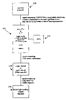
Figure 2 illustrates a block diagram of one embodiment of the present
invention for use
with a single or multi-channel lighting apparatus. An interface controller 370
provides
functionality to forward a signal comprising an (N+M)-bit binary signal
comprising a
number n, represented by the most significant N bits, and a number in,
represented by
the least significant M bits of this (N+M)-bit binary signal. The interface
controller 370
controls the extended pulse width modulator 372,, wherein the extended pulse
width
modulator generates a signal comprising an N-bit pulse width modulation signal
and
forwards it to an N-bit single or multi-channel pulse width modulation
controller 374. A
clock 373 provides the extended pulse width modulator 372 with a
synchronisation
signal having a predetermined frequency, wherein the clock 373 can be a
separate or an
integral part of the extended pulse width modulator 372. In this manner the
pulse width
modulator can process or generate dependent or multiple independent signals
for a
single or multi-channel pulse width modulation controller 374 which can
control
multiple channels of light-emitting elements such as LEDs with an effective
resolution
of 2N+m.
8
CA 02583357 2007-04-05
WO 2006/039790
PCT/CA2005/001547
The single or multi-channel pulse width modulation controller 374 can be
attached to a
single or multi-colour light-emitting element luminaire 376, wherein a multi-
colour
luminaire can comprise light-emitting elements that emit one or more light
ranges
selected from red, green, blue, amber and white, for example. Light-emitting
elements
associated with a luminaire can be categorized according to their intended
colour
impression into multiple colour channels, wherein each colour channel can have
its own
single-channel pulse width modulation controller or can be operatively
connected to one
predetermined channel of a multi-channel pulse width modulation controller.
The
single- or multi-channel pulse width modulation controller can be connected to
a single
or multi-coIour channel luminaire that can have a combination of red, green,
blue, amber
or any other coloured or otherwise categorized light-emitting elements, for
example.
A luminaire that can be controlled using the method and apparatus according to
the
present invention is illustrated as a block diagram in Figure 3. The luminaire
100
comprises a number of components including a power supply 110, a power
converter
120, a controller 140, and a light source 130. Each component comprises an
input for
receiving an input signal, and an output for providing an output signal,
however only
selected inputs and outputs of these components are illustrated in Figure 3.
Under
operating conditions the power supply 110 requires a certain form of
electrical power at
its input and provides a form P of electrical power at its output. The output
of the power
supply 110 is connected to the input of the power converter 120, wherein the
power
converter 120 transforms the electrical power P provided at its input into an
electrical
drive current I which the power converter 120 provides at its output. This
electrical
drive current 1 is provided to the light source 130 for operation thereof. The
controller
140 is operatively coupled to the power converter 120, wherein the controller
140
provides a drive current control signal Is to the power converter 120. The
controller 140
comprises or is adapted for connection to the control apparatus according to
the present
invention, thereby enabling the controller 140 to control the power converter
120 with a
resolution level of 2N '1'1 states. Furthermore, the controller 140 can be
responsive to
signal Id provided at an (optional) interface input or other input means for
example. For
example, Id can be a user desired dimming sequence.
It would be readily understood that a light source 130 can comprise one or
more arrays
of a plurality of light-emitting elements. For example the arrays can be red
LEDs, green
9
CA 02583357 2013-06-28
LEDs and blue LEDs or any other colour as would be readily understood, for
example
white LEDs or amber LEDs. A power Converter 120 can comprise one or more
current
drivers wherein for example a current driver can be configured to provide
electrical
drive current to a selected array of light-emitting elements.
In another embodiment a luminaire that can be controlled using the method and
apparatus according to the present invention can further comprise a feedback
system as
illustrated in Figure 4. The luminaire 200 comprises a power supply 110, a
power
converter 120, a controller 140, and a light source 130. The luminaire 200
additionally
comprises any combination of a sensor system 250 and a drive current sensor
system
260.
The sensor system 250 can sense any combination of one or more input
parameters. The
parameters can represent one or more of a portion of the heat Q resulting from
the
operation of the luminaire or a portion of the spectral density e(2,.) of the
light emitted by
light source 130. The sensor system can process the input parameters .which
can be
indicative of the temperature of a number of components of the light source or
the
amount and spectral composition of the light emitted by the light source,
wherein the
amount and spectral composition of the light emitted by the light source can
be provided
in chromaticity and brightness coordinates, for example. The sensor system 250
can
provide any combination of g(Q) or h(e(k)) at one or more outputs which are
operatively
connected to corresponding feedback inputs of the controller 140.
The drive current sensor system 260 may additionally be a portion of the
feedback
system of the luminaire 200. The drive current sensor system 260 can sense the
drive
current I, and provide a measure of its magnitude at its output and this
signal can be
transmitted to the controller 140. The controller 140 can provide 16 to the
power
converter 120 accounting for one or more of the sensed input signals,
including heat,
chromaticity, brightness and drive current in addition to any input signal
called Id.
The signal called
Id can represent any combination of measures of the desired drive current, the
desired
brightness or the desired chromaticity of the emitted light, for example. The
controller
comprises or is adapted for connection to the control apparatus according to
the present
invention, thereby enabling the controller to control the power converter 120
and thus
the light source 130 with a resolution level 0f 2M states.
CA 02583357 2013-06-28
Figure 5 illustrates a schematic of an electronic circuit 301 enabling the
extended pulse
width modulation method according to one embodiment of the present invention.
The
circuit comprises an eleven-line input bus 310 for receiving an eleven-bit
parallel input
control signal, a sync signal input line 313, an init signal input line 315,
and an eight-bit
output bus 319 for providing the parallel output control signal to a
compatible eight-bit
PWM controller, which is not shown. The circuit includes an exception handling
sub-
circuit comprising an eight-input NAND gate 320 and a two-input AND gate 322.
Eight
lines of the eleven-line input bus for carrying the eight most significant
bits of the input
control siorl are accordingly connected to the first port 331 of an eight-bit
adder 330.
The input line 333 of the second port of the eight-bit adder carrying the
least significant
bit is connected to the output 325 of the two-input AND gate 322 which also
constitutes
the output of the exception handling sub-circuit. The remaining seven lines of
the
second port are not shown and are set to arithmetic zero. Depending on the
adder device
this can be done by either connecting these lines to arithmetic high or
arittunetic low
voltage. Three lines of the eleven-line input bus for carrying the three least
significant
bits of the input control signal are connected to the three control signal
input lines 341 of
a three-bit programmable counter 340. The three-bit programmable counter
further has
a clock signal input 343 and a reset signal input 345 connected to the
respective lines of
the circuit as illustrated in Figure 5 for receiving the respective signals
under operating
conditions. A divide-by-eight counter 350 increments its counter upon
receiving a
predetermined change in the sync signal at its elk input 351. The counter
resets to zero
upon receiving an init or upon incrementing the counter beyond seven. The out
signal
output 353 of the divide-by-eight counter is connected to the reset signal
input 345 of
the three-bit programmable counter. When the divide-by-eight counter 350
resets to
zero, an out signal output on its out signal line resets the three-bit
programmable counter
340 via its reset signal input. The three-bit programmable counter 340
increments its
counter upon detection of a predetermined state change in the sync signal and
compares
the counter value with the number encoded in the three-bit input control
signal. When
the counter value exceeds the encoded number, its output 347 changes from
logical one
to logical zero and the output of the attached two-input AND gate 322 will be
zero.
, For the embodiment illustrated in Figure 5, under operational conditions the
exception
handling sub-circuit prevents the extended pulse width modulation circuit from
incrementing an already maximal binsry number encoded in the eight most
significant
11
CA 02583357 2007-04-05
WO 2006/039790 PCT/CA2005/001547
bits of the input control signal. This is achieved by setting the least
significant bit of the
second port of the adder input signal to zero, i.e. by AND combining the
output of the
eight-input NAND gate and the output of the three-bit programmable counter
when the
eight most significant bits represent the number 28¨ 1 (generally 211 -1).
It would be readily understood by a worker skilled in the art that the total
number of bits,
the number of most significant bits and the number of least significant bits
of the input
control signal can be different from the ones specified above. For example,
the above
circuit can be adapted for attaching a ten-bit P'WM controller using an input
control
signal having ten most significant bits and a predetermined number of least
significant
bits necessary to achieve a desired effective PWM resolution,
Furthermore, as would be obvious to a person skilled in the art, the circuit
for extended
pulse width modulation can also include input or output signal buffer elements
such as
latches, registers, and multiplexers. The circuit can be modified for example
for
receiving input signals or providing output signals on systems other than
parallel bus
systems.
In one embodiment, an incrementer can be used in place of the eight-bit adder
identified
in the above circuit. The incrementer can have one control signal input port,
for
example a single eight bit input port, and increments the number represented
by a signal
applied to the control signal input port by one, upon detection of a
predetermined state
change in a trigger signal applied to a trigger signal port which would occur
under
operating conditions.
Figure 6 illustrates a schematic of electronic circuit 300 enabling the
extended pulse
width modulation method according to another embodiment of the present
invention,
wherein the divide-by-eight counter as seen in Figure 5, has been removed.
This
embodiment uses fewer components and can be used if a sudden state change in
the
input control signal always happens synchronously when the three-bit counter
resets to
zero, for example or if a state change in the input control signal happens
asynchronously
and the action of instantaneously resetting the three-bit programmable counter
390 is not
required. Taking into account the pulse cycle duration or frequencies for
general
lighting purposes the asynchronous state change generally does not need any
exception
handling, since state changes in the input control signal typically occur on a
timescale of
12
CA 02583357 2007-04-05
WO 2006/039790
PCT/CA2005/001547
multiples rather than fractions of eight pulse cycles (generally 2m pulse
cycles). The
circuit 300 may produce, due to state changes in the input control signal
other than at the
beginning of an eight pulse cycle period (generally 2m pulse cycle period),
averaged
pulse width duty factors which deviate from the specified duty factor encoded
in the
eleven bit (generally (N+M)-bit) input control signal by no more than an
equivalent of a
single least significant bit change in the input control signal.
Figure 7 illustrates a schematic of another embodiment of an electronic
circuit 400
enabling the extended pulse width modulation method, wherein the exception
handling
sub-circuit as illustrated in Figure 5, has been eliminated. In this
embodiment, when all
eight most significant bits (generally N most significant bits) are set to
logical high, the
eight bit adder or incrementer "overflows" i.e. resets its output signals to
zero.
Depending on the number m encoded in the three least significant bits
(generally M least
significant bits) of the input control signal, this circuit sets all output
signals to logical
zero for a period of m predetermined changes in the sync signal (pulse cycles)
and sets
the output signals to logical one for a subsequent eight minus m pulse cycles
(generally
(2m ¨ m) pulse cycles) provided that the input control signals do not change
during the
total period of eight pulse cycles (generally 2m pulse cycles). The circuit
illustrated in
Figure 7 can be used for example, when it is not required to suppress such an
overflow
condition, or when the eight most significant bits (generally N most
significant bits) of
the input control signal never concurrently assume their logical high
(arithmetical one)
values.
In another embodiment, the extended PWM controller can be implemented in
firmware
as shown in Figures 8 to 10 for use with, for example, a Philips LPC2132
microcontroller.
Figure 8 illustrates a microcontroller main_PWM function 500 according to one
embodiment of the present invention. This function specifies the function
PWM_TimerISR as a PWM period timer internipt service routine, initializes
static
variable offset to zero, allocates two blocks of random access memory called
DataBank0 and DataBankl, wherein each block comprises N words of M bits, and
marks DataBank0 as active. The function then enters a continuous loop wherein
it
polls an external device, such as a remote interface, for available PWM data.
Alternatively, the data may also be generated within main_PWM program 500.
When
13
CA 02583357 2007-04-05
WO 2006/039790
PCT/CA2005/001547
PWM data which comprises an N+M-bit word is available, the main _PWM program
calls the UpdatePWMData function.
Figure 9 illustrates the UpdatePWMData function 600 according to one
embodiment
of the present invention, wherein this function first determines which data
bank is
active, then selects the inactive data bank to write any subsequent data to.
It then sets
loop counter i to zero and sets msb as the N most significant bits and lsb as
the M
least significant bits of the N+M signal before performing N loops, wherein
within each
loop it sets the ith memory location of the selected data bank to msb+1 if i
is less than
lsb, else it sets the ith memory location to msb. Upon completion, it marks
the active
data bank as inactive and the inactive data bank as active before returning to
the calling
function ma in_PWM.
Figure 10 illustrates the PWM period timer interrupt service routine
PWM_TimerISR
700 according to one embodiment of the present invention, wherein this routine
first
determines which data bank is active5-and-then selects-the active data bank to
read data
from. It then reads the off setth element of the active data bank, sets the
PWM period
timer hardware register to this value, and increments the static variable
offset. If
offset is then equal to N, it is reset to zero. The timer interrupt flag is
then cleared
and the interrupt function PWM_TimerISR exits.
In one embodiment, the present invention can be applied to pulse code
modulation
(PCM) rather than PWM. Having specific regard to Figure 2, the PWM controller
374
can be replaced with a PCM controller. A PCM based embodiment can be
implemented
with a firmware controlled general-purpose microcontroller, for example, a
Philips
LPC2132 microcontroller. This implementation is illustrated in Figures 1 ito
13.
Figure 11 illustrates a microcontroller main_PCM function 800 according to one
embodiment of the present invention. This function specifies the function
PCM_TimerISR as a periodic timer interrupt service routine, initializes static
variables
Count and Offset to zero, Mask to 1, and timer Delay to T (where T is
typically
one microsecond), allocates two blocks of random access memory called
DataBank0
and Dat aBan kl, wherein each block comprises N words of M bits, and marks
DataBank0 as-active. - The-function-then-enters a continuous loop wherein it
polls an
external device, such as a remote interface, for available PCM data.
Alternatively, the
14
CA 02583357 2013-06-28
data may also be generated within the main_PCM function (not illustrated).
When PCM
data comprising an N+M-bit word is available, the main_PCM function calls the
UpdatePCMData function.
Figure 12 illustrates the UpdatePCMData routing function 900 according to one
embodiment of the present invention, wherein this function first determines
which data
bank is active, then selects the inactive data bank to write any subsequent
data to. It
then sets loop counter i to zero and sets msb as the N most significant bits
and lab as
the M least significant bits of the N+M signal before performing N loops,
wherein
within each loop it sets the 1thmemory location of the selected data bank to
msb+1 if
i is less than 1 sb, else it sets the i memory location to rasb. Upon
completion, it
marks the active data bank as inactive and the inactive data bank as active
before
returning to the calling function ma in_ PCM
Figure 13 illustrates the periodic timer interrupt service routine
PCM_TimerISR 1000
according to one embodiment of the present invention, wherein this routine
first
determines which data bank is active, and then selects the active data bank to
read data
from. It then reads the of f se tth element of the active data bank and
performs a logical
AND with the static mask variable to determine the count& bit of the element.
If the
bit is zero, the LED channel is disabled; otherwise, it is enabled. If count
is less than
M, then the static variable count is incremented, the static variable mask is
multiplied
by two to effect a logical left shift of the binary bit, and the static
variable delay,
which represents the timer delay, is multiplied by two. Otherwise, count is
reset to
zero, mask is reset to one, delay is reset to T, and the static variable
offset is
incremented. When offset is then equal to N, it is reset to zero. Finally, the
timer
interrupt flag is cleared and the interrupt function PCM_TimerISR exits.
In one embodiment of the present invention, pulse widths can be defined in
control
coordinates (n,m,N,M). It would be obvious to a worker skilled in the art that
all such
pulse widths can be transformed into a time domain by merely applying a simple
coordinate transformation. For example, a pulse width pw whose duration is
specified
by a specific PWM control number n can have a time duration of, for example,
pw =
(2N-1).1 * n * PW in which PW is the period of the pulse cycle. Alternatively,
the
transformation can also be defined by 241 * (n * PW); the specific choice is a
mere
matter of choosing the zero origin for n.
CA 02583357 2007-04-05
WO 2006/039790
PCT/CA2005/001547
In one embodiment of the present invention, the control method can be
implemented in
an apparatus or system having one or more output channels to jointly or
separately
control each channel either simultaneously or in a time-multiplexed fashion,
wherein
each channel can be used to drive a certain color of light-emitting elements,
for example.
The invention will now be described with reference to specific examples. It
will be
understood that the following examples are intended to describe embodiments of
the
invention and are not intended to limit the invention in any way.
EXAMPLES
It is known that pulse width modulation of light-emitting elements for example
LEDs,
for solid-state luminaires must have a PWM frequency of at least about 300 Hz
to avoid
the perception of visual flicker and a PWM duty factor resolution of at least
12 bits, and
preferably a PWM frequency of at least about 10 kHz to alleviate the
detrimental effects
of thermal stress on the LED dies. The following examples illustrate the
application of
the present invention to the control and operation of solid-state luminaires.
As may be
readily understood, a multiplicity of phosphor-coated white light LEDs for
example may
be controlled by one controller, while a plurality of red, green, blue, and
optionally
amber LEDs or white, green, and blue LEDs for example may be controlled by a
multiplicity of controllers, with preferably one controller for each LED
color.
EXAMPLE 1: Solid-State Luminaire with Extended Pulse Code Modulation Control
According to one embodiment of the present invention a solid-state lighting
luminaire
can be configured as illustrated in Figure 4, wherein the extended pulse width
modulation as defined above is implemented in firmware on the controller 140,
for
example a commercial rnicrocontroller, by using the extended pulse code
modulation
method as illustrated Figures 11 to 13. One or more calibrations are
implemented on the
controller resulting from collected data reflecting one or more of
chromaticity, luminous
flux, temperature of the LEDs and drive current, thereby enabling feedback
control of
the solid-state luminaire.
16
=
CA 02583357 2013-06-28
EXAMPLE 2: Solid-State Luminaire with Extended Pulse Width Modulation Control
According to one embodiment of the present invention a solid-state lighting
luminaire
can be configured as illustrated in Figure = 4, wherein the extended pulse
width
modulation as defined above is implemented in firmware on the controller 140,
for
. example a commercial microcontroller, by using the extended pulse width
modulation
method as illustrated Figures 8 to 10. The controller can comprise one or a
plurality of
integrated 10-bit analog-to-digital converter modules, wherein other functions
may also
be implemented, such as for example sensor monitoring and feedback control.
EXAMPLE 3: Solid-State Luminaire with Extended Pulse Code Modulation Control
Referring to Figure 4, the extended pulse width modulation method disclosed
herein
may be implemented in the controller 140 using the extended pulse width
modulation as
disclosed in Figures 11 to 13 implemented in hardware using for example a
field-
programmable gate array (RIGA) with preferably a microcontroller core. Other
functions may be implemented within the luminaire including for example sensor
monitoring and feedback control.
It is obvious that the foregoing embodiments of the invention are exemplary
and can be
varied in many ways.
As such, the scope of the claims should not be limited by the particular
embodiments
or examples set forth herein, but should be given the broadest interpretation
consistent
with the description as a whole.
17