Language selection

Search

Patent 2583899 Summary

Third-party information liability

Some of the information on this Web page has been provided by external sources. The Government of Canada is not responsible for the accuracy, reliability or currency of the information supplied by external sources. Users wishing to rely upon this information should consult directly with the source of the information. Content provided by external sources is not subject to official languages, privacy and accessibility requirements.

Claims and Abstract availability

Any discrepancies in the text and image of the Claims and Abstract are due to differing posting times. Text of the Claims and Abstract are posted:

  • At the time the application is open to public inspection;
  • At the time of issue of the patent (grant).
(12) Patent: (11) CA 2583899
(54) English Title: SHIELDED MICROPHONE FOR MOBILE COMMUNICATIONS DEVICE
(54) French Title: MICRO BLINDE POUR DISPOSITIF DE COMMUNICATION MOBILE
Status: Granted and Issued
Bibliographic Data
(51) International Patent Classification (IPC):
  • H05K 09/00 (2006.01)
  • H04R 01/00 (2006.01)
  • H04R 01/02 (2006.01)
(72) Inventors :
  • PHILLIPS, ROBERT W. (Canada)
(73) Owners :
  • RESEARCH IN MOTION LIMITED
(71) Applicants :
  • RESEARCH IN MOTION LIMITED (Canada)
(74) Agent: NORTON ROSE FULBRIGHT CANADA LLP/S.E.N.C.R.L., S.R.L.
(74) Associate agent:
(45) Issued: 2011-03-08
(22) Filed Date: 2007-04-04
(41) Open to Public Inspection: 2007-10-07
Examination requested: 2007-04-04
Availability of licence: N/A
Dedicated to the Public: N/A
(25) Language of filing: English

Patent Cooperation Treaty (PCT): No

(30) Application Priority Data:
Application No. Country/Territory Date
06112357.6 (European Patent Office (EPO)) 2006-04-07

Abstracts

English Abstract


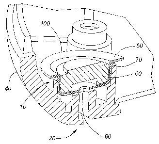
A shielded microphone, and method for shielding a microphone, are provided for
use in a communications device having a circuit board and a microphone,
especially where the device also has an antenna in close proximity to the
microphone. The microphone is provided in an electromagnetic shield (e.g.
formed as a shielding can) and a resilient separator (e.g. o-ring or disk) is
provided over the shield. The device housing is stacked over the separator and
shield, while the latter are stacked over the circuit board so that the
separator and
shield, with microphone there under, are sandwiched between the housing and
the circuit board. By this sandwiching the separator is loaded onto the shield
to
drive the shield directly against the circuit board to make an electrical
ground
connection therewith, the microphone also being electrically connected to the
printed circuit board. The microphone is thereby enclosed between the circuit
board and the shield, such that the shield shields the microphone against
electromagnetic energy radiated by the proximate antenna. The resilience of
the
separator accommodates the variation in the stacking of the components.


French Abstract

L'invention porte sur un micro blindé et sur le procédé de blindage connexe. Ce micro est destiné à servir dans un dispositif de communication mobile équipé d'une carte de circuits imprimés et d'un micro, notamment lorsque ledit dispositif est aussi muni d'une antenne montée tout près du micro. Le micro est logé dans un réceptacle offrant une protection électromagnétique (p. ex. une boîte de blindage) et muni d'un séparateur résilient (joint torique ou disque) monté sur le blindage. Le boîtier du dispositif est monté par dessus le séparateur et le blindage, alors que ce dernier est placé au dessus de la carte de circuits imprimés, le micro étant pris en sandwich entre le boîtier et la carte. En empilant ainsi les composants, le séparateur appuie sur le blindage de façon à pousser celui-ci contre la carte de circuits pour la mettre à la masse, le micro étant aussi branché à la carte de circuits. Ce dernier se trouve donc coincé entre la carte de circuits et le blindage qui l'isole de l'énergie électromagnétique diffusée par l'antenne avoisinante. La résilience du séparateur laisse un jeu suffisant pour l'empilage des composants.

Claims

Note: Claims are shown in the official language in which they were submitted.


8
Claims:
1. A shielded microphone assembly comprising a microphone and a
conductive, electromagnetic shield, for use in a communications device having
a
circuit board and a housing, and in use being proximate to an antenna,
characterized by a resilient separator over said electromagnetic shield,
wherein
said conductive, electromagnetic shield is over said microphone and said
assembly is configured to co-operate with said housing and said circuit board
to
electrically connect each of said microphone and said electromagnetic shield
to
said circuit board upon loading said housing onto said separator and said
electromagnetic shield onto said circuit board, thereby enclosing said
microphone between said circuit board and said electromagnetic shield and
grounding said electromagnetic shield.
2. A shielded microphone assembly according to claim 1, wherein said
electromagnetic shield is formed as a shielding can having a lip, said
shielding
can electrically connecting to said circuit board by means of said lip.
3. A shielded microphone assembly according to claim 2, wherein said
separator is a resilient o-ring surrounding an outside perimeter of said
shielding can over said lip.
4. A shielded microphone assembly according to claim 1, wherein said
electromagnetic shield is formed as a shielding can and said separator is a
resilient disk positioned over a ceiling of said shielding can, said ceiling
configured for positioning adjacent said housing upon said loading of said
housing.
5. A shielded microphone assembly according to claim 4, wherein said disk
is aligned over said shielding can, upon said loading of said housing, by
means
of a channel formed in said housing.

9
6. A shielded microphone assembly according to any one of claims 1-5,
wherein said separator comprises an electrically insulating material.
7. A shielded microphone assembly according to any one of claims 1-6,
wherein said circuit board is a printed circuit board.
8. A shielded microphone assembly according to any one of claims 1-7,
wherein said electromagnetic shield comprises an outlet for communication of
sound waves to said microphone.
9. A shielded microphone assembly according to claim 4 or claim 5, wherein
said disk comprises a central aperture for communication of sound waves to
said
microphone.
10. A mobile communications device comprising an antenna and a shielded
microphone assembly in accordance with any one of claims 1 to 9.
11. A method of shielding a microphone in a communications device
having a circuit board and a housing, said device being used with an antenna
either as part of said device or in proximity to said device, the method
comprising
shielding said microphone with a conductive, electromagnetic shield over said
microphone and characterized by the steps of:
providing a resilient separator over said electromagnetic shield; and
sandwiching said shielded microphone and separator between said
housing and said circuit board,
whereby said shielded microphone and separator are configured to co-
operate with said housing and said circuit board to electrically connect each
of
said microphone and said electromagnetic shield to said circuit board, said
electromagnetic shield being thereby grounded, said sandwiching producing a
loading of said housing onto said separator and said electromagnetic shield
onto
said circuit board, thereby enclosing said microphone between said circuit
board

and said electromagnetic shield.
12. A method according to claim 11, whereby said electromagnetic shield is
formed as a shielding can having a lip, said shielding can electrically
connecting
to said circuit board by means of said lip.
13. A method according to claim 12, whereby said separator is a resilient o-
ring provided to surround an outside perimeter of said shielding can.
14. A method according to claim 11, whereby said electromagnetic shield is
formed as a shielding can and said separator is a resilient disk provided over
a
ceiling of said shielding can, said ceiling being positioned adjacent said
housing
upon said loading of said housing.
15. A method according to any one of claims 11 to 14, whereby said separator
comprises an electrically insulating material.
16. A method according to any one of claims 11 to 15, whereby said
electromagnetic shield comprises an outlet for communication of sound waves to
said microphone.
17. A method according to any one of claims 11 to 16, whereby said
microphone is fixed to said circuit board and said circuit board is a printed
circuit
board.
18. A method according to any one of claims 11 to 17, whereby said
microphone is held against said circuit board by said electromagnetic shield.

Description

Note: Descriptions are shown in the official language in which they were submitted.


CA 02583899 2007-04-04
1
SHIELDED MICROPHONE FOR MOBILE COMMUNICATIONS DEVICE
Mobile, handheld communications devices typically contain a miniature
microphone such as an electret condenser microphone. In such devices, the
microphone is typically held against a printed circuit board and electrically
connects to the circuit board via a pair of small coil springs. Such devices
also
typically have an antenna in close proximity to the microphone with the
attendant
possibility that the microphone can undesirably pick up, as noise,
electromagnetic
energy radiated by the antenna. In the case of mobile telephones, this
undesirable noise is sometimes referred to in the industry as "GSM buzz". To
shield the microphone against such noise pick-up, a grounded shield
(hereinafter
alternatively referred to as an "electromagnetic shield") is typically used to
surround or enclose the microphone so as to isolate the microphone,
electromagnetically, from such radiation.
In the typical mass production of handheld, mobile communications devices, a
number of parts are stacked together and enclosed in a housing. The stack of
parts must, when fully assembled, occupy the space defined by the housing of
the
device. The variability in the size of the parts in the stack and their proper
placement during assembly requires that tolerances be factored into the design
of
the stack of parts. The pressure between the various parts in the stack
ultimately
depends upon the aggregate size of the parts made to occupy the well-defined
space. As excess pressure between the parts may cause undesirable strain and
damage thereto, resilient parts capable of absorbing the stack pressure are
typically included. Furthermore, in assembling such devices, it is important
that
the method of mounting the microphone and the electromagnetic shield onto the
circuit board be able to accommodate the tolerances of assembly while, at the
same time, ensure that an effective electrical connection is made, as
required,
between the circuit board and each of the microphone and electromagnetic
shield.
The problem of providing for both the tolerances of assembly and electrical
connection between the electromagnetic shield and circuit board have been
addressed by placing a conductive gasket between the shield and the circuit

CA 02583899 2007-04-04
2
board, with such gasket being sufficiently compliant to absorb the stack
pressure
and required assembly tolerances and the its conductivity providing an
electrical
connection between the shield and the circuit board. However, those gaskets
are
relatively expensive and their placement is critical and, thus, poses greater
difficult
during assembly of the device, since they function as an intermediary
component
between the shield and the circuit board to establish the electrical
connection
between them.
There is, therefore, a need, in a communications device having a microphone
and
an antenna in close proximity, for a shield assembly which both protects the
microphone against energy radiated by the antenna and is able to economically
achieve the necessary electrical connections that withstand manufacturing
tolerances.
BRIEF DESCRIPTION OF THE DRAWINGS
An understanding of exemplary embodiments of the invention will be obtained
from the following description, with reference to the following drawings in
which
like reference numerals refer to like components throughout:
FIG. 1 shows a cross-sectional, pictorial perspective view of an exemplary
shielded microphone assembly in accordance with one such embodiment (of
which the circuit board has been omitted to better show the remaining
components);
FIG. 2 shows a cross-sectional, pictorial plan view of the embodiment of FIG.
1 in
which an o-ring-type separator is used;
FIG. 3 shows a cross-sectional, pictorial, plan view of another exemplary
embodiment of the microphone assembly in which a gasket-type separator is
used; and,

CA 02583899 2007-04-04
3
FIG. 4 shows a flowchart illustrating steps of a method in accordance with
another
aspect of the invention for assembling a shielded microphone for mounting onto
a
circuit board.
DESCRIPTION OF PREFERRED EMBODIMENTS
In accordance with an aspect of the invention, a shielded microphone assembly
is
preferably provided for use in a communications device having a circuit board
and
a housing and having an antenna or used proximate to an antenna. The
microphone is placed inside a conductive, electromagnetic shield (e.g. a
shielding
can) and a separator (e.g. an o-ring-type) is placed over the shield, forming
an
assembly configured to co-operate with the housing and the circuit board to
electrically connect each of the microphone and the electromagnetic shield to
the
circuit board. The device housing can then be stacked over the assembly,
namely, over the shield to load the separator onto the shield and drive the
shield
directly against the circuit board, whereby the shield becomes grounded
through
an electrical connection with the circuit board. As a result, the microphone
is
enclosed between the circuit board and the electromagnetic shield, and is
shielded against electromagnetic energy radiated by the nearby antenna. Since
the separator is resilient it accommodates the variation in the stack of
parts. The
electromagnetic shield, when formed as a shielding can, may have a lip whereby
the shielding can electrically connects to the circuit board by means of the
lip.
The separator (preferably an electrical insulator), when formed as a resilient
o-
ring, preferably surrounds an outside perimeter of the shielding can over the
lip.
Or, the separator, when formed as a resilient disk, is preferably positioned
over a
ceiling of the shielding can, where the ceiling is configured to be positioned
adjacent the housing upon the loading of the housing. The electromagnetic
shield
may include an outlet for communication of sound waves to the microphone.
A further aspect of the invention preferably provides a mobile communications
device comprising an antenna and a shielded microphone assembly according to
the foregoing.

CA 02583899 2007-04-04
4
A still further aspect of the invention preferably provides a method of
shielding a
microphone in such a communications device whereby the microphone is
shielded with a conductive, electromagnetic shield; a resilient separator is
provided over the electromagnetic shield; and, the shielded microphone and
separator are sandwiched between the housing and the circuit board. The
shielded microphone and separator are configured to co-operate with the
housing
and the circuit board to electrically connect each of the microphone and the
electromagnetic shield to the circuit board, thereby grounding the
electromagnetic
shield. The sandwiching produces a loading of the housing onto the separator
and the electromagnetic shield onto the circuit board, thereby enclosing the
microphone between the circuit board and the electromagnetic shield.
The foregoing disadvantages of the known shielded microphone assemblies can
be overcome by using a shielded microphone as described herein and illustrated
by FIG.'s 1 - 4. As shown for the embodiment illustrated by Fig.'s 1 and 2,
the
shielded microphone assembly 10 can be used in any suitable communications
device 20 having a circuit board 30 (see Fig. 2), which may be a printed
circuit
board, a housing 40 and, in a mobile communications device, an antenna (not
shown). The shielded microphone assembly 10 has an electromagnetic shield in
the form of a shielding can 50, a microphone 60 and a separator 70. The
shielding can 50 is composed of a conductive material and is grounded through
an electrical connection with an electrical ground contact of the circuit
board 30.
The shielding can 50 and the circuit board 30, when in contact, define an
enclosure 80. The microphone 60 is contained within the enclosure 80 and when
installed in a communications device is electrically connected with the
circuit
board 30. The shielding can 50 and the microphone 60 may be any suitable
shape such that the microphone 60 fits within the enclosure; accordingly, the
cross-sectional shape of the shielding can 50 may be circular, square,
hexagonal
or any other suitable shape which co-operates with the shape of the microphone
and circuit board. The microphone 60 may be held against the circuit board 30
by
the shielding can 50; alternatively, the microphone 60 may be soldered or
otherwise affixed to the circuit board 30.

CA 02583899 2007-04-04
The shielding can 50 includes an outlet 90 or other means for communicating
sound waves into the shielding can 50 and, thence, to the microphone 60. The
separator 70, which is made of a resilient material and may also be insulating
(e.g. rubber), is positioned between the shielding can 50 and the housing 40.
In
5 this manner, the shielding can 50 shields the enclosed microphone 60 from
electromagnetic energy, including electromagnetic energy from a proximate
antenna, while the separator 70, being resilient, is springy and able to
rebound
from, and absorb, pressure between the housing 40 and the shielding can 50.
In the exemplary embodiment of FIG.'s 1 and 2, the separator 70 is an o-ring-
type
separator positioned over the shielding can 50 and apart from the circuit
board 30,
so as to surround the outside perimeter of the shielding can 50. The shielding
can
50 of this embodiment includes a lip 100 over which the separator 70 is
positioned
such that, when installed in a communications device by stacking these
components with the housing 40 positioned there over and the circuit board 30
positioned there under, the lip 100 of the shielding can 50 is pressed into
electrical
contact with the circuit board 30. By this stacking, the separator 70 is
sandwiched
between the housing 40 and the lip 100, and the lip 100 is sandwiched between
the separator 70 and the circuit board 30.
Alternatively, as shown in FIG. 3, the separator 70 may be a resilient disk
positioned over a shielding can 50 which does not include such a lip. In this
embodiment, the ceiling (top) 55 of the shielding can 50 parallel to the
housing 40
is sandwiched between the disk separator 70 and the circuit board 30. As shown
for this embodiment, the disk separator 70 is aligned over the shielding can
50 by
means of an appropriately sized channel 110 formed in the housing 40. Further,
the disk separator 70 may include a central aperture 57, as shown, aligned in
the
stack with the counterpart outlet 90 of the ceiling of the shielding can 50
for
communication of sound waves to the microphone 60.
The challenges associated with the known methods of assembling a shielded
microphone, as discussed above, are overcome by using the method described
herein and illustrated by the flowchart of FIG. 4. The method 120 can be used
for

CA 02583899 2007-04-04
6
the production of any suitable communications device having a circuit board,
which may be a printed circuit board, a housing and, for mobiles devices, an
antenna. The method 120 is used for assembling a shielded microphone 10 and
mounting it onto a circuit board 30, wherein the shielded microphone assembly
includes a shielding can 50 and a microphone 60. As described above, the
shielding can 50 includes means for communicating sound waves into the
shielding can 50 to the microphone 60.
The shielding can 50 and the microphone 60 are mounted together, the
microphone being placed within the shielding can, and positioned 130 on the
circuit board 30 so that both the microphone and shielding are in electrical
contact
with the circuit board 30. A resilient separator 70 is positioned 140 over the
shielding can 50. The housing 40 is stacked over and pressed onto 150 the
separator 70 so as to load the separator 70, sandwiching it between the
housing
40 and the shielding can 50. In turn, the shielding can 50 is pressed against
the
circuit board 30, whereby the shielded microphone assembly becomes mounted
on the circuit board 30. The resilience of the separator 70 enables it to
absorb
(tolerate) the load placed on it by this stacking of the housing 40 onto the
shielding can 50 and circuit board 30 there under.
Alternatively, as illustrated in Fig. 4 by step 170 shown in dotted outline to
indicate
that it replaces the foregoing step 130 for this alternative, the microphone
60 of
the shielded microphone assembly may first be mounted onto the circuit board
30
(e.g. by soldering), followed by mounting of the shielding can 50 onto the
circuit
board 30 so as to cover the microphone 60.
As compared to the solutions known heretofore, the solutions described herein
facilitate the manufacturing of such devices while at the same time reducing
the
overall cost of parts.
With the foregoing exemplary embodiments having been disclosed, it will be
apparent to those skilled in the art that various changes and modifications
can be
made to appropriately suit the needs and objectives of another application and
still

CA 02583899 2007-04-04
7
achieve the advantages of the invention; all such changes and modifications
are
intended to fall within the scope of the invention as defined by the claims
that
follow.
Note: This patent disclosure and document contains material which is subject
to
copyright protection. The copyright owner has no objection to the facsimile
reproduction of any one of the patent disclosure or patent document, as it
appears
in the Patent Office patent file or records, but otherwise reserves all
copyright
rights whatsoever.

Representative Drawing
A single figure which represents the drawing illustrating the invention.
Administrative Status

2024-08-01:As part of the Next Generation Patents (NGP) transition, the Canadian Patents Database (CPD) now contains a more detailed Event History, which replicates the Event Log of our new back-office solution.

Please note that "Inactive:" events refers to events no longer in use in our new back-office solution.

For a clearer understanding of the status of the application/patent presented on this page, the site Disclaimer , as well as the definitions for Patent , Event History , Maintenance Fee  and Payment History  should be consulted.

Event History

Description Date
Letter Sent 2024-04-04
Common Representative Appointed 2019-10-30
Grant by Issuance 2011-03-08
Inactive: Cover page published 2011-03-07
Inactive: Final fee received 2010-12-16
Pre-grant 2010-12-16
Notice of Allowance is Issued 2010-07-16
Inactive: Office letter 2010-07-16
Letter Sent 2010-07-16
Notice of Allowance is Issued 2010-07-16
Inactive: Approved for allowance (AFA) 2010-06-18
Letter Sent 2010-05-10
Revocation of Agent Requirements Determined Compliant 2010-04-26
Inactive: Office letter 2010-04-26
Appointment of Agent Requirements Determined Compliant 2010-04-26
Reinstatement Request Received 2010-04-09
Amendment Received - Voluntary Amendment 2010-04-09
Reinstatement Requirements Deemed Compliant for All Abandonment Reasons 2010-04-09
Appointment of Agent Request 2010-04-07
Revocation of Agent Request 2010-04-07
Inactive: Abandoned - No reply to s.30(2) Rules requisition 2009-09-18
Amendment Received - Voluntary Amendment 2009-09-18
Inactive: S.30(2) Rules - Examiner requisition 2009-03-18
Inactive: S.29 Rules - Examiner requisition 2009-03-18
Inactive: Cover page published 2007-10-07
Application Published (Open to Public Inspection) 2007-10-07
Inactive: First IPC assigned 2007-06-28
Inactive: IPC assigned 2007-06-28
Inactive: IPC assigned 2007-06-27
Application Received - Regular National 2007-05-03
Letter Sent 2007-05-03
Inactive: Filing certificate - RFE (English) 2007-05-03
Request for Examination Requirements Determined Compliant 2007-04-04
All Requirements for Examination Determined Compliant 2007-04-04

Abandonment History

Abandonment Date Reason Reinstatement Date
2010-04-09

Maintenance Fee

The last payment was received on 2010-04-06

Note : If the full payment has not been received on or before the date indicated, a further fee may be required which may be one of the following

  • the reinstatement fee;
  • the late payment fee; or
  • additional fee to reverse deemed expiry.

Patent fees are adjusted on the 1st of January every year. The amounts above are the current amounts if received by December 31 of the current year.
Please refer to the CIPO Patent Fees web page to see all current fee amounts.

Owners on Record

Note: Records showing the ownership history in alphabetical order.

Current Owners on Record
RESEARCH IN MOTION LIMITED
Past Owners on Record
ROBERT W. PHILLIPS
Past Owners that do not appear in the "Owners on Record" listing will appear in other documentation within the application.
Documents

To view selected files, please enter reCAPTCHA code :


To view images, click a link in the Document Description column (Temporarily unavailable). To download the documents, select one or more checkboxes in the first column and then click the "Download Selected in PDF format (Zip Archive)" or the "Download Selected as Single PDF" button.

List of published and non-published patent-specific documents on the CPD .

If you have any difficulty accessing content, you can call the Client Service Centre at 1-866-997-1936 or send them an e-mail at CIPO Client Service Centre.

({010=All Documents, 020=As Filed, 030=As Open to Public Inspection, 040=At Issuance, 050=Examination, 060=Incoming Correspondence, 070=Miscellaneous, 080=Outgoing Correspondence, 090=Payment})


Document
Description 
Date
(yyyy-mm-dd) 
Number of pages   Size of Image (KB) 
Description 2007-04-03 7 289
Claims 2007-04-03 3 104
Abstract 2007-04-03 1 26
Drawings 2007-04-03 4 62
Representative drawing 2007-09-16 1 14
Claims 2010-04-08 3 112
Abstract 2010-12-15 1 26
Commissioner's Notice - Maintenance Fee for a Patent Not Paid 2024-05-15 1 556
Acknowledgement of Request for Examination 2007-05-02 1 176
Courtesy - Certificate of registration (related document(s)) 2007-05-02 1 105
Filing Certificate (English) 2007-05-02 1 158
Notice of Reinstatement 2010-05-09 1 171
Courtesy - Abandonment Letter (R30(2)) 2010-04-25 1 164
Commissioner's Notice - Application Found Allowable 2010-07-15 1 164
Correspondence 2010-04-06 2 98
Correspondence 2010-04-25 1 18
Correspondence 2010-04-25 1 15
Correspondence 2010-12-15 2 69