Language selection

Search

Patent 2584274 Summary

Third-party information liability

Some of the information on this Web page has been provided by external sources. The Government of Canada is not responsible for the accuracy, reliability or currency of the information supplied by external sources. Users wishing to rely upon this information should consult directly with the source of the information. Content provided by external sources is not subject to official languages, privacy and accessibility requirements.

Claims and Abstract availability

Any discrepancies in the text and image of the Claims and Abstract are due to differing posting times. Text of the Claims and Abstract are posted:

  • At the time the application is open to public inspection;
  • At the time of issue of the patent (grant).
(12) Patent Application: (11) CA 2584274
(54) English Title: DICHROIC MIRROR
(54) French Title: MIROIR DICHROIQUE
Status: Deemed Abandoned and Beyond the Period of Reinstatement - Pending Response to Notice of Disregarded Communication
Bibliographic Data
(51) International Patent Classification (IPC):
  • C03C 17/34 (2006.01)
  • C03C 17/36 (2006.01)
(72) Inventors :
  • AUMERCIER, LAURENT (France)
  • DREIDEMY, PIERRE ANDRE (France)
(73) Owners :
  • FLABEG HOLDING GMBH
(71) Applicants :
  • FLABEG HOLDING GMBH (Germany)
(74) Agent: NORTON ROSE FULBRIGHT CANADA LLP/S.E.N.C.R.L., S.R.L.
(74) Associate agent:
(45) Issued:
(86) PCT Filing Date: 2005-10-27
(87) Open to Public Inspection: 2006-05-04
Availability of licence: N/A
Dedicated to the Public: N/A
(25) Language of filing: English

Patent Cooperation Treaty (PCT): Yes
(86) PCT Filing Number: PCT/EP2005/055605
(87) International Publication Number: WO 2006045835
(85) National Entry: 2007-04-16

(30) Application Priority Data:
Application No. Country/Territory Date
04105400.8 (European Patent Office (EPO)) 2004-10-29

Abstracts

English Abstract


The present invention concerns dichroïc mirrors also known as optical filters.
In particular, rear view mirrors comprising a vitreous substrate coated with a
stack of interferential layers and with a metallic reflector. The stack of
layers includes, successively from the substrate, i) one layer of a high
refractive index material in the range of 1.9 to 2.8, ii) one layer of a lower
refractive index material in the range of 1.2 to 2, iii) one layer of
semiconductor material having a refractive index of more than 3. The
refractive indexes of high refractive index materials and of the low
refractive index materials differ at least by 0.2, and the coated substrate
has a transmittance at 550 nm of at least 6%, preferably at least 8% and a
reflectance at 550 nm greater than 45%, preferably greater than 50 %.


French Abstract

L'invention concerne des miroirs dichroïques également connus sous le nom de filtres optiques, notamment des rétroviseurs comportant un substrat vitreux revêtu d'une pile de couches d'interférence et d'un réflecteur métallique. Ladite pile de couches comporte successivement, à partir du substrat, i) une couche de matériau à indice de réfraction élevé dont l'indice de réfraction est compris entre 1,9 et 2,8 ; ii) une couche de matériau à indice de réfraction faible dont l'indice de réfraction est compris entre 1,2 et 2 ; et iii) une couche de matériau semiconducteur dont l'indice de réfraction est supérieur à 3. Les indices de réfraction des couches de matériau à indice de réfraction élevé et de matériau à indice de réfraction faible différent de l'ordre d'au moins 0,2, et le substrat revêtu présente un facteur de transmission d'au moins 6 % à 550 nm, de préférence d'au moins 8 %, et un facteur de réflexion supérieur à 45 % à 550 nm, de préférence supérieur à 50 %.

Claims

Note: Claims are shown in the official language in which they were submitted.

6
CLAIMS
1.- A vitreous substrate, having a front surface and a rear surface, coated on
its rear
surface with a stack of layers including, successively from the substrate,
i) one layer of a high refractive index material in the range of 1.9 to 2.8,
ii) one layer of a lower refractive index material in the range of 1.2 to 2,
iii) one layer of semiconductor material having a refractive index of more
than 3,
- the refractive indexes of high refractive index materials and of the low
refractive index materials differing at least by 0.2,
- the optical thickness of layer i) being lower than 260 nm preferably lower
than 250 nm, and the optical thickness of layer ii) being lower than 240
nm, preferably lower than 220 and
- the coated substrate having a transmittance at 550 nm of at least 6%,
preferably at least 8% and a reflectance at 550 nm greater than 45%,
preferably greater than 50 %.
2.- coated substrate according to claim 1, characterised in that the optical
thickness of
layer i) is comprised between 85 and 240 nm, preferably comprised between 100
and 225 nm.
3.- Coated substrate according to any of the preceding claims, characterised
in that
the optical thickness of layer ii) is comprised between 50 and 180 nm,
preferably
between 60 and 170 nm.
4.- Coated substrate according to any of the preceding claims, characterised
in that it
has a transmittance at 700 nm of 38 % or less, preferably of 35% or less and a
reflectance at 700 nm of at least 43 %, preferably at least 45 %.
5.- Coated substrate according to any one of the preceding claims,
characterised in
that it has a transmittance at 800 nm of 62 % or less, preferably of 60 % or
less and
a reflectance at 800 nm of at least 22 %, preferably at least 25 %.
6.- Coated substrate according to any one of the preceding claims,
characterised in
that the semiconductor material is selected from at least one of the following
material
: silicon, chromium, germanium, titanium, aluminium, tungsten, nickel or alloy
of
these material.
7.- Coated substrate according to any one of the preceding claims,
characterised in
that the semiconductor material is silicon undoped or doped with 0 to 12% Al,
and is
at least partially cristallised.

7
8.- Coated substrate according to any one of the preceding claims,
characterised in
that the high refractive index material is selected amongst titanium oxide,
niobium
oxide, aluminium nitride and silicon nitride.
9.- Coated substrate according to any one of the preceding claims,
characterised in
that the low refractive index material is selected amongst silicon oxide,
magnesium
fluoride, tin oxide.
10.- Coated substrate according to any one of the preceding claims,
characterised in
that it has a neutral tint in reflection.
11.- Coated substrate according to any one of the preceding claims,
characterised in
that the colour in reflection present a purity lower than 13%, preferably
lower than
10%.
12.- Coated substrate according to any one of the preceding claims,
characterised in
that the layer of semiconductor material has a thickness comprises between 5
and
100 nm, preferably between 10 and 75 nm.
13.- Coated substrate according to any one of the preceding claims,
characterised in
that when layer iii) is a Cr layer, its geometrical thickness is comprised
between 5 to
50 nm, preferably between 10 and 40 nm.
14.- Coated substrate according to any one of claims 1 to 12, characterised in
that,
when layer iii) is a Si layer, its geometrical thickness is comprised between
5 and 75
nm, preferably between 10 and 60 nm.
15.- Coated substrate according to any of the preceding claims, characterised
in that
nature and thickness of layer iii) is chosen in way that if the substrate were
coated
with layer iii) alone it would have a LR measured on the non coated side of
less than
50 %, preferably less than 30%.
16.- Coated substrate according to any one of the preceding claims,
characterised in
that the layer of low refractive index material has a geometrical thickness
comprised
between 25 and 150 nm, preferably between 30 and 120 nm.
17.- Coated substrate according to any one of the preceding claims,
characterised in
that the layer of low refractive index material has a geometrical thickness
comprised
between 20 and 150 nm, preferably between 25 and 125 nm.

Description

Note: Descriptions are shown in the official language in which they were submitted.


CA 02584274 2007-04-16
WO 2006/045835 PCT/EP2005/055605
Dichroic mirror
The present invention concerns dichroic mirrors also known as optical filters.
In
particular, the invention relates to a rear view mirror comprising a vitreous
substrate
coated with a stack of interferential layers and with a metallic reflector.
Several constructions comprising a system combining a rear view mirror with a
display, an emitter and/or electromagnetic sensor hidden behind the mirror
surface
are known. In these systems, the display / emitter or sensor operates trough
the
mirror while the mirror itself reflects what is expected from its function
thanks to a
specific coating arrangement which has simultaneously (1) the ability to
reflect a
significant portion of the visible spectrum and (2) can transmit a sufficient
amount of
the electromagnetic radiations emitted by the display / emitter and / or
absorbed by
the sensor.
All these systems installed on road vehicles usually exhibit a reflectance
rate
comprised between 35 and 55% (typically measured according to SAE J964 or
equivalent procedure), and are often built with the reflecting layer(s) placed
on the
front surface of the mirror compared to the position of the observer. This
embodiment maximizes the reflectance and the transmittance simultaneously, a
quite
challenging task when they both have to cover more or less same portions of
the
electromagnetic spectrum.
In some cases, system constructions using a reflective layer on the front
surface is not
advantageous and there is therefore a need for a dichroic mirror comprising a
stack
of interferential layers on the rear surface. When using rear face
construction, the
transmittance rate is usually sacrificed on behalf of the reflectance rate.
For example,
when using a thin layer of chromium as reflector, it is known that the
following values
can be obtained :
Reflectance* % Transmittance* %
58.8 1.4
53.7 5.1
45.4 9.4
40.8 12.1
15.4
* reflectance and transmittance as measured here are according to SAE J964
procedure. They signify integrated values over the visible spectrum.
One can then understand that almost no light is transmitted once the
reflectance
35 exceeds 58-60%.

CA 02584274 2007-04-16
WO 2006/045835 PCT/EP2005/055605
2
It has been discovered that the use of a stack of interferential layers and a
suitable
metallic reflector according to the invention, on the rear surface of the
substrate, can
enhance both the transmittance and the reflectance rates.
The object of the present invention is a vitreous substrate, having a front
surface and
a rear surface, coated on its rear surface with a stack of layers including,
successively
from the substrate,
i) one layer of a high refractive index material in the range of 1.9 to 2.8,
ii) one layer of a lower refractive index material in the range of 1.2 to 2,
iii) one layer of semiconductor material having a refractive index of more
than 3,
- wherein the refractive indexes of high refractive index materials and of the
low
refractive index materials differ at least by 0.2, and
- the optical thickness (geometrical thickness X refractive index) of layer i)
being
lower than 260 nm preferably lower than 250 nm, and the optical thickness of
layer ii) being lower than 240 nm, preferably lower than 220, and
- the coated substrate having a transmittance at 550 nm of at least 6%,
preferably
at least 8% and a reflectance at 550 nm greater than 45%, preferably greater
than
50%.
Advantageously, the object of the invention is as disclosed in the dependant
claims.
The coated substrate can have a blue tint in reflection but it can also
presents a
neutral tint in reflection. In this case, the colorimetric Hunter values a*
and b* are
preferably comprises between -10 and + 10 and the purity is preferably lower
than
13 %, more preferably lower than 10%.
The system is particularly interesting in prismatic interior day/night rear
view mirrors.
The reflector has to be behind the glass to offer a high reflectance "day
position".
The front surface of the glass itself, with its own refractive index, gives
the low
reflectance level of the commonly called "night position". Simultaneously with
our
invention, the transmittance is kept at sufficient level to allow the use of
display /
emitter and/or sensor devices placed behind the mirror.
The invention can also be used in "self dimming", sometime called
"electrochromic"
automatic day/night rear view mirrors where the highest possible reflectance
of the
mirror is required to increase the device optical range.
Such system can be applied on any suitable transparent substrate (for example
glass
or plastic), by all known means from the state of the art for such
construction, for
example dipping, pyrolitic deposition process as Chemical Vapor Deposition
(CVD),
or Physical Vapor Deposition (PVD) or the combination of any of these
techniques.
Another interesting advantage of our constructions is to be durable so as to
permit
manufacturing handling without deterioration (mechanical - scratch resistance)
and
to have a substantial self protection against corrosion (climatic stability).

CA 02584274 2007-04-16
WO 2006/045835 PCT/EP2005/055605
3
Examples
In the following examples, rear view dichroic mirrors was formed by coating
the rear
face (the face opposite of the observer) of a sodo-lime glass substrate with
different
stack of layers. The layers are deposited by magnetically enhanced vacuum
sputtering deposition process. In a way commonly known by the skilled man, the
glass passed through successive deposition chambers where the appropriate
targets
materials are bombarded under vacuum.
Example 1 :
The coated substrate, viewed form the observer, consists in :
Glass 2 mm / Ti02 60nm / Si02 50nm / Cr 20nm
This structure gives the following optical characteristics :
reflectance at 550 nm 63%
transmittance at 550 nm 6%
transmittance at 400 nm 8%
transmittance at 700 nm 12 %
transmittance at 800 nm 15%
Other interesting combinations exist with the same materials when their
respective
thickness are in the range of
Glass (0.4 to 6 mm) / Ti02 (30 to100nm) / Si02 (30 to 100nm) / Cr (10 to 30nm)
Example 2:
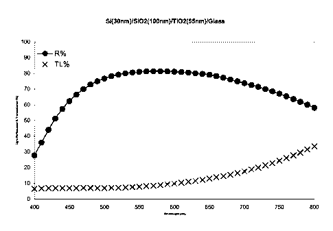
The structure is similar to that of example 1, but for the reflector, Silicium
is used
instead of Chromium.
Glass 2 mm / Ti02 55nm / Si02 100nm / Si 30nm
The following optical characteristics are obtained (see spectral data in fig.
1)
reflectance at 550 nm 81%
transmittance at 550 nm 8%
transmittance at 400 nm 7%
transmittance at 700 nm 18 %
transmittance at 800 nm 34%
The Silicium refraction and absorption indexes over the visible and near infra
red
spectrum are such that a thinner layer may be used.
Simultaneously other interesting combinations also exist with the same
materials
when their respective thickness are in the range of

CA 02584274 2007-04-16
WO 2006/045835 PCT/EP2005/055605
4
Glass (0.4 to 6 mm) / Ti02 (55 to100nm) / Si02 (30 to 100nm) / Si (15 to 50nm)
Example 3:
Glass / Ti02 (60 nm) / Si02 (60nm) / Si (30nm)
The following optical characteristics are obtained (see spectral data in fig.
2):
reflectance at 550 nm 70 %
transmittance at 550 nm 12 %
transmittance at 400 nm 10 %
transmittance at 700 nm 31 %
transmittance at 800 nm 56 %
The coated substrate shows a neutral tint in reflection (a*=-8, b*=+9, purity
is
8.5%)
Example 4
Glass 2 mm / Ti02 60nm / Si02 60nm / Si 15 nm
The following optical characteristics are obtained (see spectral data in fig.
3)
reflectance at 550 nm 60 %
transmittance at 550 nm 20 %
transmittance at 400 nm 8%
transmittance at 700 nm 64 %
transmittance at 800 nm 81 %
Example 5
Glass 2 mm / Ti02 60nm / Si02 60nm / Si 50 nm
The following optical characteristics are obtained (see spectral data in fig.
4)
reflectance at 550 nm 65 %
transmittance at 550 nm 11 %
transmittance at 400 nm 1 %
transmittance at 700 nm 19 %
transmittance at 800 nm 32 %
Example 6
Glass 2 mm / Ti02 100nm / Si02 30nm / Si 30nm

CA 02584274 2007-04-16
WO 2006/045835 PCT/EP2005/055605
The following optical characteristics are obtained (see spectral data in fig.
5)
reflectance at 550 nm 62 %
5 transmittance at 550 nm 16 %
transmittance at 400 nm 4%
transmittance at 700 nm 32 %
transmittance at 800 nm 56 %
An alternative to above embodiments consists in the use of, instead of
Silicium,
Silicium doped with another metal in the amount of less than 15%.
Such mean being a classical choice in the state of the art in PVD to improve
its
deposition process, as long as the optical properties are not substantially
affected,
one can prefer to use doped Silicium, for example with 2% to 12% Aluminium
combined with the Silicium, whether it is Si02 or Si layer.
All our embodiments can receive on their uttermost rear face a coating of
paint /
enamel / other material, typically of a thickness above one micron to even
further
improve their mechanical / corrosion / anti shatter behaviour. Upon request
suitable
"windows" in front of display / emitter / sensor shall be placed locally.

Representative Drawing
A single figure which represents the drawing illustrating the invention.
Administrative Status

2024-08-01:As part of the Next Generation Patents (NGP) transition, the Canadian Patents Database (CPD) now contains a more detailed Event History, which replicates the Event Log of our new back-office solution.

Please note that "Inactive:" events refers to events no longer in use in our new back-office solution.

For a clearer understanding of the status of the application/patent presented on this page, the site Disclaimer , as well as the definitions for Patent , Event History , Maintenance Fee  and Payment History  should be consulted.

Event History

Description Date
Application Not Reinstated by Deadline 2009-10-27
Time Limit for Reversal Expired 2009-10-27
Deemed Abandoned - Failure to Respond to Maintenance Fee Notice 2008-10-27
Letter Sent 2007-10-02
Inactive: Multiple transfers 2007-08-13
Inactive: Cover page published 2007-06-28
Inactive: Notice - National entry - No RFE 2007-06-26
Inactive: First IPC assigned 2007-05-09
Application Received - PCT 2007-05-08
National Entry Requirements Determined Compliant 2007-04-16
Application Published (Open to Public Inspection) 2006-05-04

Abandonment History

Abandonment Date Reason Reinstatement Date
2008-10-27

Maintenance Fee

The last payment was received on 2007-04-16

Note : If the full payment has not been received on or before the date indicated, a further fee may be required which may be one of the following

  • the reinstatement fee;
  • the late payment fee; or
  • additional fee to reverse deemed expiry.

Please refer to the CIPO Patent Fees web page to see all current fee amounts.

Fee History

Fee Type Anniversary Year Due Date Paid Date
MF (application, 2nd anniv.) - standard 02 2007-10-29 2007-04-16
Basic national fee - standard 2007-04-16
Registration of a document 2007-08-13
Owners on Record

Note: Records showing the ownership history in alphabetical order.

Current Owners on Record
FLABEG HOLDING GMBH
Past Owners on Record
LAURENT AUMERCIER
PIERRE ANDRE DREIDEMY
Past Owners that do not appear in the "Owners on Record" listing will appear in other documentation within the application.
Documents

To view selected files, please enter reCAPTCHA code :


To view images, click a link in the Document Description column. To download the documents, select one or more checkboxes in the first column and then click the "Download Selected in PDF format (Zip Archive)" or the "Download Selected as Single PDF" button.

List of published and non-published patent-specific documents on the CPD .

If you have any difficulty accessing content, you can call the Client Service Centre at 1-866-997-1936 or send them an e-mail at CIPO Client Service Centre.


Document
Description 
Date
(yyyy-mm-dd) 
Number of pages   Size of Image (KB) 
Drawings 2007-04-16 5 1,097
Representative drawing 2007-04-16 1 213
Description 2007-04-16 5 204
Claims 2007-04-16 2 99
Abstract 2007-04-16 2 184
Cover Page 2007-06-28 1 176
Notice of National Entry 2007-06-26 1 195
Courtesy - Abandonment Letter (Maintenance Fee) 2008-12-22 1 173
PCT 2007-04-16 6 191