Note: Descriptions are shown in the official language in which they were submitted.
CA 02584571 2014-05-29
Doc No: 10-612 CA
Patent
STAGGERED VERTICAL COMB DRIVE FABRICATION METHOD
CROSS-REFERENCE TO RELATED APPLICATIONS
[001] The present invention claims priority from U.S. Patent No. 7,357,874
having priority
date of April 12th, 2006.
TECHNICAL FIELD
[002] The present invention relates generally to vertical comb drive
actuators and to
methods of fabrication thereof, and more particularly to a method of
fabrication of an efficient
vertical staggered comb drive actuator with improved alignment tolerances.
BACKGROUND OF THE INVENTION
[003] A staggered vertical comb drive (SVCD) is a type of MEMS (Micro-
Electro
Mechanical Systems) actuator capable of relatively high actuator strength and
a high speed using
electrostatic principal of operation. Furthermore, they can be fabricated
using standard materials
and scalable processes developed in the semiconductor industry. SVCDs can be
advantageously
used to control high-speed, high-resolution micromirrors in a variety of
optical applications
including optical scanning, optical switching, free-space optical
communications, optical phased
arrays, optical filters, external cavity lasers, adaptive optics and other
applications.
[004] The actuation principle of a typical SVCDs is electrostatic. A
potential difference is
applied between two comb structures, a movable comb, or a rotor, and a
stationary comb, or a
stator. When a voltage is applied between them, the movable comb (rotor) is
drawn toward the
stationary comb (stator) until the teeth of the stator and rotor overlap and
the electrostatic field
energy is minimized. Different types of SVCD devices are described in further
detail, for
example, in US Patent 6,612,029 to Behin et al.
[005] FIG. 1 illustrates a typical prior art SVCD 20. The SVCD 20 includes
a stator 22 and
a rotor 30. The stator has individual comb fingers 24 formed on a spine 26.
The rotor 30 includes
individual comb fingers 32 linked by a spine 34. The rotor 30 also includes a
mirror or
-1-
CA 02584571 2007-04-11
Doc No: 10-612 CA
Patent
paddle 40 with associated torsional hinges 42. In a resting state the rotor 30
is positioned
substantially above the stator 22 as shown in FIG. 1.
[006] FIG. 2 illustrates the SVCD system 20 in an activated state. This
state is achieved by
applying a voltage between the rotor 30 and the stationary comb assembly 22.
In this state, the
individual combs of the rotor and stator interdigitate. The applied voltage
attracts the rotor 30 to
the stator 22, thus exerting torque on the torsional hinges 42, forcing the
mirror 40 to tilt. The
torsional hinges 42, which are anchored, provide restoring torque when the
voltage is removed.
[007] A typical prior art process flow involves creating the moving comb
assembly 30 by
etching one silicon-on-insulator (SOT) wafer, and the stationary comb assembly
22 by etching
another SOI wafer, and then assembling, for example bonding, the etched wafers
together to
form the SVCD 20. Different versions of such process are described in US
Patents 6,925,710,
7,079,299, etc. However, stringent alignment requirements between the two
wafers from which
the two comb assemblies are formed can considerably complicate the device
processing and
negatively affect the device yield.
[008] Alignment of the stator and rotor fingers is critical to proper
operation of the actuator.
Failure to achieve the required alignment can impair the actuator performance
and/or reliability
as a result of failure modes such as electrical breakdown, mechanical
interference, and lateral
collapse.
[009] Typically the rotor and stator must be aligned laterally, i.e. in the
plane of the wafer
and the combs, to approximately one micron or better. However, when the rotor
and stator are
fabricated from different wafers, accuracy of a front side to back side wafer
alignment, and of the
lateral alignment of the wafer bond can be of the order of three microns (3
sigma) across a wafer.
[0010] To overcome this difficulty, techniques have been proposed for self-
aligned
manufacturing of the rotor and stator fingers, wherein both the rotor and
stator a
photolithographically fabricated from a same device layer of a SOT wafer.
- 2 -
If
CA 02584571 2007-04-11
Doc No: 10-612 CA
Patent
[0011] For example, US Patent 6,612,029 to Behin, et al discloses a method
of simultaneous
fabrication of the rotor and stator fingers from the same device layer that
includes two
conductive silicon layers separated by an isolation layer of a silicon oxide.
The final device has
at least one set of fingers, for example of the rotor, each of which has two
vertically stacked
conductive layers separated by the isolation oxide layer. In operation, one of
said conductive
layers is grounded, and the voltage is applied to the other to create a
pulling electrical field
between said layer and the adjacent fingers of the stator which are grounded.
The stator fingers
can be etched down to the isolation layer to form a thinned set of stator
fingers. In one
embodiment, the isolation oxide layer is removed leaving an air gap in the
respective fingers.
[0012] Although the SVCD fabrication method disclosed by Behin et al
provides self-aligned
rotor and stator, it has other disadvantages. One disadvantage of this method
is that the multi-
layer fingers it forms may suffer from electrical breakdown at high voltages,
which effectively
limits the applied voltage and thereby - the rotation angle of the rotor. This
limitation can be
especially severe if the oxide layer separating the conducting layers of the
fingers is removed,
forming the air gap; additionally, the air gap embodiment can be sensitive to
the presence of
small dust particles, which can electrically shorten the device. If the oxide
layer is not removed,
its electrical properties can drift over time; for example, it can accumulate
static electrical charge
over time altering the electric field coupling the stator and rotor, leading
to undesirable variations
and/or aging of the device performance.
[0013] US Patent application 2007/0026614 to Choo, et al discloses an SVCD
fabrication
method which is somewhat similar to the method of Behin et al, but wherein the
device layer
from which the rotor and stator are fabricated in a single conductive silicon
layer without the
isolating oxide layer in the middle, using a two-layer mask to separately
define the rotor and
stator fingers. One set of the fingers is thinned by a timed etch process to
about half of the device
layer height, while the other set remains full-height. Although the resulting
device is free from
the disadvantages of the Behin SVCD discussed hereinabove, it has others. One
disadvantage of
the method of Choo et al is that it results in a device with a reduced
rotation angle of the rotor,
since the applied voltage can only rotate the rotor until a middle point of
its fingers is aligned
with a middle point of the stator fingers. For example, in the device of Choo,
the middle points
- 3 -
,
CA 02584571 2007-04-11
Doc No: 10-612 CA
Patent
of the rotor and stator fingers in a rest state, when no voltage is applied,
are separated only by
about a quarter of the device layer height, as opposed to the separation of
about a half of the
device layer height for the device of Behin.
[0014] An object of the present invention is to provide a self-aligned
method of fabrication
of SVCD devices that are free from all or at least some of the above described
and other
disadvantages of the prior art methods.
SUMMARY OF THE INVENTION
[0015] In accordance with the invention, a method is provided for
fabricating a staggered
vertical comb drive, the method comprising the steps of: a) providing a wafer
comprising a
device layer, b) etching the device layer to form therein two comb structures
comprising a first
set of fingers interdigited with a second set of fingers, c) removing a top
portion of each finger
from the first set of fingers by etching, so as to vertically shorten the
first set of fingers, and
attaching a carrier wafer to the device layer for supporting thereof, and d)
removing a lower
portion of each finger from the second set of fingers by etching from a back
side of the wafer, so
as to vertically shorten the second set of fingers resulting in said second
set of fingers being
vertically offset from the first set of fingers.
[0016] In one embodiment, step d) comprises the step of first forming a
third mask on the
back side of the wafer to protect the first set of fingers during the etching
in step (d), and to
expose to said etchings the lower portions of the second set of fingers.
[0017] In accordance with another feature of this invention, the step of
forming the two-layer
mask comprises the steps of: al) forming a first mask over the device layer so
as to expose
portions thereof corresponding to the first set of fingers, a2) disposing,
over the device layer and
the first mask, a masking layer which is substantially resistant to an etch
process used in step (b);
and, a3) removing portions of the masking layer to form a second mask defining
fingers of the
first and second sets and exposing portions of the wafer therebetween.
¨ 4 ¨
CA 02584571 2007-04-11
Doc No: 10-612 CA
Patent
[0018]
In a preferred embodiment of the invention the device layer is conductive, the
wafer
further comprising an isolation layer sandwiched between the device layer and
a base layer,
which is at least partially removed prior to step (d).
BRIEF DESCRIPTION OF THE DRAWINGS
[0019]
The invention will be described in greater detail with reference to the
accompanying
drawings which represent preferred embodiments thereof, wherein:
[0020]
FIG. 1 is an isometric diagram of a prior art staggered vertical comb drive
(SVCD) in
a resting state;
[0021]
FIG. 2 is an isometric diagram of the prior art SVCD shown in FIG.1 in an
activated
state;
[0022] FIGs. 3A-3H are cross-sectional schematic diagrams illustrating the
fabrication of an
SVCD device according to an embodiment of the present invention;
[0023] FIG. 31 is an exemplary legend of materials used in the fabrication
process illustrated
in FIGs. 3A-3H;
[0024]
FIG. 4 is a schematic diagram illustrating a plane view of the SVCD device
which
fabrication is illustrated in FIGs. 3A-3H;
[0025]
FIG. 5 is a cross-sectional schematic diagram of a portion of the SVCD device
fabricated according to the present invention showing a vertical gap, not to
scale, between the
stator and rotor fingers;
[0026]
FIGs.6A, 6B are cross-sectional schematic diagrams illustrating the
fabrication of an
SVCD device according to an embodiment of the present invention using an etch
stop layer.
DETAILED DESCRIPTION
[0027]
A preferred embodiment of the method for fabricating an SVCD device according
to
the present invention is illustrated in FIGs. 3A-3H and is hereafter described
with reference to an
SVCD device 88, a plane view of which is shown in FIG.4; FIG.3I shows an
exemplary legend
- 5
' ' Ir
CA 02584571 2007-04-11
Doc No: 10-612 CA
Patent
of materials used in the fabrication method of the present invention. One
skilled in the art will
however appreciate that the method of the present invention can be
advantageously employed
using a different set of materials, and for fabrication of many other types of
SVCD devices
having vertically offset features requiring precise lateral alignment.
100281
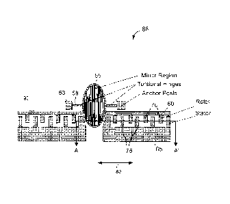
As shown in this FIG.4, the SVCD 88 includes a mirror 55, which is rotatable
about
torsional hinges 58 anchored by anchor posts 53. The mirror 55 is coupled to a
movable comb
assembly 60, hereinafter referred to as the rotor 60, which has a set of comb
teeth, hereinafter
referred as fingers 70. The rotor fingers 70 are positioned in-between fingers
75 of a stationary
comb assembly 65, hereinafter referred to as the stator 65. The sets of stator
and rotor fingers 75,
70 in the process of their fabrication will be referred to hereinafter as the
first and second sets of
fingers.
100291
According to an exemplary embodiment of the present invention described
hereinbelow, the SVCD 88 is fabricated from a silicon-on-isolator (SOD wafer
90; FIGs. 3A-3H
illustrate the fabrication process in one embodiment of the invention by
schematically showing,
at different stages of the processing, a vertical cross-section of a portion
of the SOT wafer 90
along the AA' cross-section line indicated in FIG. 4.
100301
With reference to FIG. 3A, the SOI wafer 90 is provided in a first step of the
method;
it has an isolation layer 110 of silicon oxide, hereinafter referred to also
as the oxide layer 110,
sandwiched between a base layer 100 supporting the structure, and a device
layer 120, in a
preferred embodiment both made of silicon. An arrow 128 indicates a side of
the wafer 90
wherein the device layer 120 is located; it will be referred to hereinafter as
the front side 128 of
the wafer 90, with the opposite side of the wafer referred to as the back side
129, as indicated by
a respectively labeled arrow. As described hereinbelow, the method of the
present invention
involves selectively etching of the device layer 120 from both the front and
back side of the
wafer 90.
[0031]
First, a two-layer mask 125 is formed over a front side 128 of the device
layer 120;
the two-layer mask 125 covers portions of the device layer from which the sets
of rotor and
stator fingers are to be formed, and exposes for etching portions 111 of the
device layer 120
between said eventual rotor and stator fingers, as illustrated in FIG. 3A.
- 6
' Ir
CA 02584571 2007-04-11
Doc No: 10-612 CA
Patent
[0032]
In one embodiment, the two-layer mask 125 is formed as follows. A first
masking
layer 105, which is indicated in FIGs. 3A-C in white, for example one of
silicon oxide, silicon
nitride, aluminum, photoresist or other suitable material, is disposed over
the device layer 120
and photolithographically patterned to form a first mask 126, which exposes
portions of the
device layer 120 from which the first set of fingers will be formed in the
following steps, and
covers portions of the device layer from which a second set of fingers will be
formed. In the
embodiment described herein, the first set of fingers corresponds to fingers
70 of the rotor 60,
and the second set of fingers corresponds to fingers 75 of the stator 65. In
other embodiments,
the first set of fingers can be stator fingers, while the second set of
fingers can be rotor fingers.
[0033]
Next, a second masking layer 115, for example of a photoresist, is disposed
over the
device layer 120 and the first mask 126. The first and second masking layers
contain different
types of masking material, so that one can be selectively removed without
substantially affecting
the other. Portions of the second masking layer 115 are then selectively
removed, for example
using photolithography, according to a second pattern to form a second mask
127 defining
locations of the first and second sets of fingers; more particularly, it
covers portions of the
device layer 120 which will eventually become the rotor fingers 70 and stator
fingers 75, and
exposes portions 111 of the device layer 120 and, optionally, of the first
mask 126, between the
locations of adjacent fingers of the first and second sets of fingers.
Portions of the first mask 126
that are not covered by the second mask 127 defining the locations of the
first and second sets of
fingers are also removed using an etch process to which the second mask is
resistant, i.e. has a
substantially smaller etch rate, so as to align the first and second mask
patterns over portions of
the device layer 120 wherefrom the second set of fingers is formed, and to
expose for etching the
device layer 120 between locations of adjacent fingers of the first and second
sets.
Advantageously, the first and second masks 126, 127 formed by this process are
self-aligned in
lateral direction, as indicated by an arrow 80, over the locations of the
second set of fingers,
while the locations of the first set of fingers are protected, i.e. covered,
only by the second mask
127, which defines both the rotor and the stator finger locations.
100341
Next, in one embodiment of the invention the device layer 120 is etched to a
desired
first depth d1, for example by using a timed deep reactive-ion etch (DRIE) or
another suitable
method of deep etching to form two comb structures with the first set of
fingers 140 interdigited
- 7
CA 02584571 2007-04-11
Doc No: 10-612 CA
Patent
with the second set of fingers 150, as illustrated in FIG. 3B. The desired
first depth d1 is
preferably about half of the thickness d of the device layer 120, d1 0.5d, but
can be either
smaller or larger than 0.5d in other embodiments. This etch step will be
hereinafter referred to as
the first DRIE etch step, or the first DRIE etch. The second mask 127 is
subsequently removed to
expose the first set of fingers 150 to etching.
100351
Turning now to FIG. 3C, a second etch of the front side of the wafer 90 is
performed
following the removal of the second mask 127, for example in a DRIE etcher, to
etch through the
device layer 120 between adjacent fingers of the first and second sets of comb
fingers 150, 140,
stopping at the oxide layer 110. After this step, the second set of fingers
140 extends
substantially through the whole device layer 120 up to the oxide layer 110.
Simultaneously, this
second etch step removes a top portion of each un-masked finger from the first
set of fingers 150,
thereby vertically shortening, or thinning the first set of fingers 150 in a
vertical direction
indicated by an arrow 95. After this step, the first set of fingers 150 now
extends from the oxide
layer 110 in the vertical direction only to a fraction, e.g. about one half or
less, of the thickness d
of the device layer 120, as illustrated in FIG.3C. The second etch step may be
timed to stop
when a desired height 113 of the second set of fingers 150 is reached.
100361 The processing steps that produce the structure shown in FIG.3C
involve, substantially, i)
etching of the device layer to form two comb structures comprising the first
set of fingers 150
interdigited with the second set of fingers 140, and ii) removing a top
portion of each finger from
the first set of fingers 150 by etching to provide the first set of vertically
shortened fingers
interdigited with the second set of fingers. One skilled in the art would
appreciate that these tasks
can also be performed using an alternative etch process than that described
hereinabove. For
example, during the first DRIE etch step, the device layer 120 can be etched
through up to the
oxide layer 110, e.g. using the oxide layer 110 as an etch stop, so as to
result in all the fingers
from the first and second sets 140 and 150 being of the same height d, which
can then be
followed by the removal of the second mask 127 as described hereinabove, and a
timed DRIE
etch to remove the top portions of each finger from the first set of fingers
150 while leaving the
second set of fingers 140 substantially intact.
100371
Turning back to FIG. 3C, in a next step a carrier wafer 160 is attached, e.g.
by fusion
wafer bonding or using any other suitable wafer bonding or gluing method, to
the front side 128
- 8
CA 02584571 2007-04-11
Doc No: 10-612 CA
Patent
of the device layer 120, from which the first and second etch DRIE steps
described hereinabove
were performed, resulting in the formation of the two sets of fingers 140, 150
of different height
as described hereinabove. By way of example, the carrier wafer 160 is a
silicon wafer, preferably
having a suitably isolating layer not shown herein, for example formed by
silicon oxide for
electrical isolation from the stator, but can also be a glass wafer, or may be
made of any other
suitable material strong enough for supporting the resulting SVCD structure.
Optionally, the first
mask 126 can be removed prior to bonding of the wafers 90 and 160. FIG. 3D
illustrates the
resulting two-wafer structure 99 wherein the device layer 120 is now supported
by the carrier
wafer 160, which preferably has recesses 231, 232 for accommodating, i.e. not
impeding, the
vertical motion of the mirror 55 and, optionally, of the first set of fingers
150, i.e. the rotor
fingers, when the SVCD 88 is actuated by an applied voltage.
[0038]
Turning now to FIG. 3E, in a next step the base layer 110 of the wafer 90 is
at least
partially thinned and removed, e.g. by anisotropic or isotropic etching, so as
to expose the oxide
layer 110 and, ultimately, the lower portions of the fingers 140 for etching;
the words "lower
portion" herein refer to a portion of a comb finger 140 that is closest to the
back side 129 of the
wafer 90.
100391
Next, in FIG. 3F a third mask 170 is formed, for example with a photoresist,
over the
back side 129 of the wafer 90 on the exposed oxide layer 110, so as to protect
the first set of
fingers 150 during subsequent etching, and to expose to said etching portions
172 of said back
side 129 of the wafer 90, or in the shown embodiment - portions of the oxide
layer 110,
underlying the second set of fingers 140. Advantageously, lateral alignment
accuracy of the third
mask 170 with respect to the locations of the second set of fingers 140 can be
rather relaxed, as
the required lateral positioning accuracy of openings in the mask 170 over the
fingers 140 is in
the order of a nominal distance between adjacent fingers of the first and
second sets 140, 150,
said distance being typically larger than the finger width, and typically
exceeds two microns. By
way of example, fingers of the first and second sets have each a width of 3
tm, the lateral
distance between adjacent rotor and stator fingers 150, 140 is 4 pm, and the
thickness of the
device layer d is 20
- 9
'Ir
CA 02584571 2007-04-11
Doc No: 10-612 CA
Patent
[0040]
With a reference to FIG. 3G, in a next step the back side 129 of the wafer 90
is etched
to remove the oxide layer 110 where it is not covered by the third mask 170,
so as to expose
fingers of the first set 140 from the back side of the wafer. Subsequently, a
lower portion of each
exposed finger of the first set 140 is removed, e.g. in a DRIE etcher during a
third DRIE etch
step by etching to a second depth d2, to vertically shorten, or make thinner
the second set of
fingers 140. The removal of the exposed oxide layer 110 not covered by the
mask 170 may be
performed in the same DRIE etch process that is employed for the thinning of
the second set of
fingers 140, or alternatively using a separate anisotropic or non-anisotropic
etching process as
would be known to those skilled in the art.
[0041]
Advantageously, the step of thinning of fingers of the second set 140 by
etching from
the back side 129 of the wafer 90 results in the first and second sets of
fingers 150, 140 being
vertically offset relative to each other, thereby increasing a vertical
distance between mid-points
of adjacent fingers of the first and second sets 150 and 140, thereby
enhancing the actuation
range of the resulting SVCD device 88 illustrated in FIG. 4. As stated
hereinabove, in the
embodiment described herein the first and second sets of fingers 150 and 140
correspond to the
rotor and stator fingers 70, 75 respectively,
[0042]
Turning now to FIG. 3H, in a next processing step the third mask 170 and the
remaining oxide layer 110 are removed, and a reflective layer 205, for example
of a metal such
as gold, is deposited via an opening 215 in a shadow mask 210 over a mirror
region 55' of the
device layer 120, said mirror region 55' coupled to the first set of fingers
150, to form the
reflective mirror 55 as shown in FIG.4.
[0043]
In another embodiment, the reflective layer 205 can be deposited over the
oxide layer
110 after the removal of the base layer 100 as shown in FIG. 3E, and used,
after patterning with a
photoresist, to form the mask 170, which is then employed for reducing the
vertical thickness of
the second set of fingers 140, i.e. of the stator, as described hereinabove
with reference to FIGs.
3F and 3G. The metal layer and the oxide layer 110 are then removed everywhere
but the mirror
region 55'.
[0044]
The aforedescribed fabrication steps illustrated in FIGs. 3A-3H, which result
in the
formation of the SVCD device 88, illustrate the method of the present
invention in one
¨10¨
' 'Ir
CA 02584571 2007-04-11
Doc No: 10-612 CA
Patent
exemplary embodiment thereof. The method has several important advantages
compared to the
prior art. First, it automatically provides laterally aligned fingers of the
first and second sets 150,
140, i.e. of the rotor and stator combs, since both sets of fingers are
fabricated from the same
device layer using a single mask, i.e. the second mask 127, which alone
defines the lateral
locations of both the stator and the rotor fingers. As a result, the method
provides precise rotor-
stator lateral alignment using standard photolithography. Furthermore, the
method of the present
invention enables one to control a vertical alignment of the rotor and stator
fingers 150, 140 by
controlling the first and second etch depths d1 and d2. For example, the
fingers 140, 150 can be
fabricated so that at zero applied voltage, i.e. with the SVCD in a resting
state, there is a small
and uniform vertical gap 222 therebetween as shown in FIG.5, so as to provide
a suitably large
angular range of the stator movement while maintaining a suitably low
operating voltage.
Advantageously, the present method enables a greater control of said vertical
gap 222 compared
to the prior art vertical comb actuator described in US Patent 6612029, as the
gap 222 in the
SVCD device 88 is not subject to limitations due to electrical shorting.
Simultaneously, the
greater vertical offset between the stator and rotor fingers afforded by the
present invention
provides for an increased angular range of the rotor movement compared to an
actuator wherein
the rotor and stator fingers substantially overlap in the vertical direction,
e.g. as the one described
in US Patent Application 2007/0026614.
[0045]
The present invention has been described hereinabove with reference to a
particular
embodiment thereof; however one skilled in the art will appreciate that the
method of the present
invention can also be advantageously practiced in other embodiments. For
example, although the
wafer 90 is referred to hereinabove as the SOI wafer, and the described
embodiment of the
method uses the silicon device layer 120 to form the rotor and stator of the
SVCD device, in
other embodiments the conductive device layer 120 and the base layer 100 may
be made of other
suitable materials including, but not limited to silicon, silicon-germanium,
silicon-carbide, other
semiconductor materials, or metals such as nickel, and gold. The insulating
layer 110, which is in
the aforedescribed preferred embodiment is silicon oxide, for example formed
by thermal
oxidization of the base silicon layer 100, in other embodiments may be
alternatively made of any
suitable insulating material including, but not limited to, silicon-nitride,
silicon-oxide, silicon-
carbide, quartz, high resistivity silicon, high resistivity silicon germanium,
polyimide, or a
polymeric film. Other substrates and combinations of materials may also be
used in different
-11
,
CA 02584571 2014-05-29
Doc No: 10-612 CA
Patent
fabrication processes realizing the method of the present invention. Also by
way of example, the
hinges 58, hereinabove referred to as torsional, can be alternatively embodied
using serpentine
hinges or other suitable types of hinges.
[0046] FIGs. 6A and 6B illustrate another embodiment of the invention,
wherein the device
layer 120 incorporates an etch stop layer 313, for example embodied as a
silicon oxide layer, at a
desired depth to control the etch depth during the second and, possibly, the
first DRIE etch steps
when portions of the first set of fingers 150 are removed. The same etch stop
layer can
subsequently be used in a third etch step which removes lower portions of the
second set of
fingers 140. This results in a structure shown in FIG. 6B, wherein the use of
the etch stop layer
313 provides uniform height of fingers of the first and second sets 140, 150
across the wafer, and
uniform vertical gap 222' between conducting portions of adjacent fingers,
which size is
advantageously controlled by the thickness of the etch stop layer 313.
[0047] Furthermore, one skilled in the art will appreciate that processing
steps leading to the
formation of the SVCD device 88 can be performed in a different order than
that described
hereinabove with reference to FIGs. 3A-3H. For example, the processing can
start with
performing a single-step timed DRIE etch of the device layer 120 of the wafer
90 front the front
side 128 thereof to remove portions of the device layer 120 up to a
predetermined depth at lateral
locations of the first set of fingers 150, with a mask alignment tolerance in
this step being
relatively relaxed. After the front side of the wafer is bonded to the support
wafer 160 and
thinned, the two-step DRIE etch is performed, substantially as described
hereinabove with
reference to FIGs. 3B and 3C using a self-aligned two-layer mask such as the
mask 125, but
from the back side of the device layer 120 to form two self-aligned sets of
fingers 140, 150,
substantially as shown in FIG.3H.
[0048] Of course numerous other embodiments may be envisioned from the
teachings in the
current disclosure without departing from the scope of the invention, as
defined by the appended
claims.
-12-