Note: Descriptions are shown in the official language in which they were submitted.
CA 02585064 2007-04-23
WO 2006/049936 PCT/US2005/038240
VOLTAGE MONITORING FOR CONNECTED
ELECTRICAL ENERGY STORAGE CELLS
FIELD OF THE INVENTION
[0001] The present invention relates generally to circuits for charging and
balancing
voltages of energy storage cells connected in series stacks, and, more
particularly, to
circuit for monitoring voltages of individual rechargeable cells of a module.
BACKGROUND
[0002] Energy storage devices are often constructed as individual cells
connected in
series. The series connected cells may be disposed within a module such that
the module
provides a nominal operating voltage higher than those available from each
individual
cell. When charging a module, different rates of accepting charge can cause
some of the
cells to have higher voltages than other cells. Similarly, individual cells
may have
different discharge characteristics and internal leakage currents, causing
voltage
differences on individual cells during discharge cycles and during periods of
module
inactivity (periods of storage, for example). Voltage differences across cells
of the same
module are problematic for at least the following two related reasons.
[0003] First, voltage differences can cause some cells to be charged to a
higher than
rated voltage. Excessive voltage (overvoltage) on a cell can shorten the
cell's life, and,
consequently, shorten the life of the module. Overvoltage can also cause
catastrophic
failure of the cell and, thus, the module. To avoid such failures, many
manufacturers of
modules provide a safety margin, with the maximum module voltage rating set
below the
sum of the voltage ratings of the constituent cells. This approach lowers the
energy
capacity of the module. Furthermore, voltage differences can accumulate during
a
1
CA 02585064 2007-04-23
WO 2006/049936 PCT/US2005/038240
module's service life, eventually causing overvoltage when the module is
charged.
Providing a reasonably small safety margin is therefore not a foolproof
solution.
[0004] Second, overvoltage on some cells may cause lower than average voltage
(undervoltage) in other cells. The cells with low voltages then accept less
energy and are
underutilized, also resulting in a lower stored energy capacity of the module.
[0005] It follows that, ideally, all cells of a module should be identical, so
that the
cells accept and release electrical charge at the same rate, and have voltages
that closely
track each other. In practice, however, cell characteristics may vary
significantly from
cell to cell. This is particularly true when the cells have not been "matched"
to each
to other. Matching cells of a module is an additional step in a module
manufacturing
process, which increases the cost of a module. Moreover, the original match is
hardly
ever perfect; and the closer the specified match, the costlier the matching
step becomes.
Equally important, even closely-matched cells may age differently, with
increasing
divergence in their performance characteristics over both charge-discharge
cycles and
chronological age.
[0006] To reduce the problems associated with voltage imbalances of individual
cells, some modules employ voltage balancers across the cells, also known as
voltage
equalizers. These devices help to keep the cell-to-cell voltage variations
relatively low.
Voltage equalizers known in the art include flyback circuits, shunt circuits,
and switched
capacitor circuits.
[0007] The presence of a voltage equalizer does not necessarily prevent cell
overvoltage. For example, the entire module can still be overcharged,
resulting in an
overvoltage being equally distributed across all cells of the module. This is
particularly
true in case of a voltage equalizer that removes charge from cells with
relatively high
voltages and transfers the removed charge to the cells with relatively low
voltages. Such
is typically the case with some flyback circuit equalizers and switched
capacitor
equalizers.
2
CA 02585064 2007-04-23
WO 2006/049936 PCT/US2005/038240
[0008] In some applications, voltage monitoring circuits connected to each
individual
cell can be used to monitor individual cell voltages in order to reduce the
possibility of
cell overvoltage, as well as for other reasons. Voltage monitoring can be used
alone, or
in combination with voltage equalization. For example, some shunt voltage
equalizers
include voltage monitors that control parallel connections (shunts) across
individual cells.
When a cell's voltage exceeds some preset level, the shunt across that cell is
activated,
limiting current flowing into the cell, or draining current from the cell. But
voltage
monitoring in a voltage equalizer circuit is limited to a comparison against a
single
reference threshold. Moreover, known voltage equalizers do include voltage
monitoring
circuits for individual cells, and/or do not provide outputs for reading cell
voltages.
Therefore, a need arises to include a circuit for monitoring voltages of
individual cells
even in applications where a voltage equalizer is already present' but,
providing a
separate circuit for monitoring voltage of each individual cell can be rather
expensive,
especially in case of modules with a large number of cells.
[0009] Because a total module voltage can be much higher than the voltage of
an
individual cell, providing a single circuit for monitoring the total voltage
of the module,
i.e., the combined voltage of a series combination of cells, does not solve
the problem of
overvoltage of individual cells. For example, modules with 42- and 50- volt
nominal
outputs are already available or should soon become available. A circuit
capable of
monitoring a high module voltage would require components with relatively high
voltage
ratings, which adversely affects the cost of the monitoring circuits, their
complexity, and
precision.
[0010] Thus, it would be desirable to improve upon the limitations of the
prior art.
3
CA 02585064 2007-04-23
WO 2006/049936 PCT/US2005/038240
SUMMARY
[0011] A need thus exists for circuits that can be used to monitor voltages of
each
energy storage cell in a series combination of cells, but without the
accompanying
expense of building a separate circuit for each cell. Another need exists for
circuits that
can be used to monitor voltages of each energy storage cell in a module, and
that do not
require components rated for the total module voltage.
[0012] The present invention includes an electrical device that includes at
least one
voltage equalizer and a voltage monitoring circuit. The at least one voltage
equalizer can
be configured to balance individual cell voltages of a plurality of energy
storage cells
connected in series, and the voltage monitoring circuit can be configured to
monitor
voltage of a subset of the plurality of energy storage cells. The subset
includes fewer
than all cells of the plurality of energy cells. The device may further
include the plurality
of energy storage cells, such as double layer capacitor cells. In some
exemplary
embodiments, the voltage monitoring circuit provides one or more indications
when the
voltage of the subset of the cells crosses reference voltages. For example,
the voltage
monitoring circuit can provide a first indication when the voltage of the
subset exceeds a
first reference voltage, and provides a second indication when the voltage of
the subset
exceeds a second reference voltage. In other exemplary embodiments, the
voltage
monitoring circuit provides real-time indications of the voltage of the
subset. The real-
time indications can be provided continuously or continually, i.e., at some
predefined
time intervals.
[0013] In one embodiment, an electrical device comprises at least one voltage
equalizer configured to balance individual cell voltages of a plurality of
energy storage
cells connected in series; and a voltage monitoring circuit configured to
monitor voltage
of a subset of the plurality of energy storage cells, wherein the subset
comprises fewer
than all cells of the plurality of energy cells. The voltage monitoring
circuit may be
capable of providing a first indication when the voltage of the subset crosses
a first
reference voltage. The voltage monitoring circuit may be further capable of
providing a
4
CA 02585064 2007-04-23
WO 2006/049936 PCT/US2005/038240
second indication when the voltage of the subset crosses a second reference
voltage. The
voltage monitoring circuit may be capable of providing a first indication when
the
voltage of the subset exceeds a first reference voltage. The voltage
monitoring circuit
may be further capable of providing a second indication when the voltage of
the subset
exceeds a second reference voltage. The voltage monitoring circuit may be
capable of
providing a real-time indication of the voltage of the subset. The voltage
monitoring
circuit may be capable of providing a real-time continual indication of the
voltage of the
subset. The voltage monitoring circuit may be capable of providing a real-time
continuous indication of the voltage of the subset. The cells may provide
energy for
driving a vehicle, wherein the voltage monitoring circuit is capable of
providing readings
indicative of the voltage of the subset, the electrical device further
comprising a circuit
capable of transforming the readings into an estimate of remaining driving
range of the
vehicle. The at least one voltage equalizer may consist of a single voltage
equalizer. The
at least one voltage equalizer may comprise a plurality of voltage equalizers.
The at least
one voltage equalizer may comprise a first voltage equalizer; and the first
voltage
equalizer and the voltage monitoring circuit may be built as a single unit.
Each voltage
equalizer of the plurality of voltage equalizers may be configured to balance
voltages of
two adjacent cells of the plurality of energy storage cells. The plurality of
energy storage
cells may comprise more than two energy storage cells; and the voltage
monitoring
circuit may be configured to monitor voltage of exactly two energy storage
cells. The
voltage monitoring circuit may be powered by the voltage of the subset of the
plurality of
energy storage cells. The voltage monitoring circuit may be powered by voltage
of fewer
than all cells of the plurality of energy storage cells. The at least one
voltage equalizer
may have balancing capability at least an order of magnitude greater than
imbalance
introduced by current drawn by the voltage monitoring circuit. The at least
one voltage
equalizer may have balancing capability exceeding imbalance due to a sum of
maximum
design current drawn by the voltage monitoring circuit and maximum design
imbalance
that can arise in operation of the cells. The at least one voltage equalizer
may comprise a
shunt equalizer. The at least one voltage equalizer may comprise a flyback
equalizer. The
at least one voltage equalizer may comprise a switched capacitor equalizer.
The at least
one voltage equalizer may comprise an active balancer circuit. The at least
one voltage
5
CA 02585064 2007-04-23
WO 2006/049936 PCT/US2005/038240
equalizer may comprise a balancing circuit connected between a positive
terminal of one
energy storage cell and a negative terminal of a second energy storage cell.
[0014] In one embodiment, an electrical device comprises a plurality of energy
storage cells connected in series; at least one voltage equalizer configured
to balance
individual cell voltages of the plurality of energy storage cells; and a
voltage monitoring
circuit configured to monitor voltage of a subset of the plurality of energy
storage cells,
wherein the subset comprises fewer than all cells of the plurality of energy
cells. Each
cell of the plurality of energy storage cells may comprise a double layer
capacitor. The
voltage monitoring circuit may be capable of providing a first indication when
the
voltage of the subset crosses a first reference voltage. The voltage
monitoring circuit may
be further capable of providing a second indication when the voltage of the
subset crosses
a second reference voltage. The voltage monitoring circuit may be capable of
providing a
first indication when the voltage of the subset exceeds a first reference
voltage. The
voltage monitoring circuit may be further capable of providing a second
indication when
the voltage of the subset exceeds a second reference voltage. The voltage
monitoring
circuit may be capable of providing a real-time indication of the voltage of
the subset.
The voltage monitoring circuit may be capable of providing a real-time
continual
indication of the voltage of the subset. The voltage monitoring circuit may be
capable of
providing a real-time continuous indication of the voltage of the subset. The
voltage
monitoring circuit may be capable of providing readings indicative of the
voltage of the
subset, the electrical device further comprising a circuit capable of
transforming the
readings into an estimate of remaining driving range of the vehicle. The at
least one
voltage equalizer may comprise a single voltage equalizer. The at least one
voltage
equalizer may comprise a plurality of voltage equalizers. The plurality of
voltage
equalizer may comprise a first voltage equalizer; and the first voltage
equalizer and the
voltage monitoring circuit may be built as a single unit. Each voltage
equalizer of the
plurality of voltage equalizers may be configured to balance voltages of two
adjacent
cells of the plurality of energy storage cells. The plurality of energy
storage cells may
comprise more than two energy storage cells; and the voltage monitoring
circuit may be
configured to monitor voltage of exactly two energy storage cells. The voltage
monitoring circuit may be powered by the voltage of the subset of the
plurality of energy
6
CA 02585064 2007-04-23
WO 2006/049936 PCT/US2005/038240
storage cells. The voltage monitoring circuit may be powered by voltage of
fewer than all
cells of the plurality of energy storage cells. The at least one voltage
equalizer may have
balancing capability at least an order of magnitude greater than imbalance
introduced by
current drawn by the voltage monitoring circuit. The at least one voltage
equalizer may
have balancing capability exceeding imbalance due to a sum of maximum design
current
drawn by the voltage monitoring circuit and maximum design imbalances that can
arise
in operation of the cells. The at least one voltage equalizer may comprise a
shunt
equalizer. The at least one voltage equalizer may comprise a flyback
equalizer. The at
least one voltage equalizer may comprise a switched capacitor equalizer.
1o [0015] In one embodiment, a method comprises providing a plurality of
energy
storage cells connected in series; balancing individual cell voltages of the
plurality of
energy storage cells; and monitoring voltage of a subset of the plurality of
energy
storage cells, wherein the subset comprises fewer than all cells of the
plurality of energy
cells. The step of monitoring may comprise providing a first indication when
the voltage
of the subset crosses a first reference voltage. The step of monitoring may
further
comprise providing a second indication when the voltage of the subset crosses
a second
reference voltage. The step of monitoring may comprise providing a first
indication when
the voltage of the subset exceeds a first reference voltage. The step of
monitoring may
further comprise providing a second indication when the voltage of the subset
exceeds a
second reference voltage. The step of monitoring may comprise providing a real-
time
indication of the voltage of the subset. The step of monitoring may comprise
providing a
real-time continual indication of the voltage of the subset. The step of
monitoring may
comprise providing a real-time continuous indication of the voltage of the
subset. The
cells may provide energy for driving a vehicle, wherein the step of monitoring
comprises
providing readings indicative of the voltage of the subset, the method further
comprising
transforming the readings into an estimate of remaining driving range of the
vehicle. The
step of balancing may comprise using a single voltage equalizer to balance the
individual
cell voltages. The step of balancing may comprise using a plurality of voltage
equalizers
to balance the individual cell voltages. The step of monitoring may comprise
using a
voltage monitoring circuit; Therein the plurality of voltage equalizers
comprises a first
voltage equalizer; and wherein the first voltage equalizer and the voltage
monitoring
7
CA 02585064 2007-04-23
WO 2006/049936 PCT/US2005/038240
circuit are built as a single unit. The step of using may comprise utilizing
each voltage
equalizer of the plurality of voltage equalizers to balance voltages of two
adjacent cells of
the plurality of energy storage cells. The step of providing may comprise
providing more
than two energy storage cells; and the step of monitoring may comprise
monitoring
voltage of exactly two energy storage cells. The step of monitoring may
comprise using a
voltage monitoring circuit powered by the voltage of the subset of the
plurality of energy
storage cells. The step of monitoring may comprise using a voltage monitoring
circuit
powered by voltage of fewer than all cells of the plurality of energy storage
cells. The
step of balancing may comprise using a voltage equalizer with balancing
capability at
least an order of magnitude greater than imbalance introduced by current drawn
of the
voltage monitoring circuit. The step of balancing may comprise using a voltage
equalizer
with balancing capability exceeding imbalance due to a sum of imbalance caused
by
maximum design current drawn by the voltage monitoring circuit and maximum
design
imbalance that can arise in operation of the cells. The step of balancing may
comprise
using a shunt equalizer. The step of balancing may comprise using a flyback
equalizer.
The step of balancing may comprise using a switched capacitor equalizer. Each
energy
storage cell of the plurality of energy storage cells may comprise a double
layer
capacitor.
(0016] These and other features and aspects of the present invention will be
better
understood with reference to the following description, drawings, and appended
claims.
8
CA 02585064 2007-04-23
WO 2006/049936 PCT/US2005/038240
BRIEF DESCIRPTION OF THE FIGURES
[0017] Figure 1 is a high-level illustration of a combination of a series
stack of
energy storage cells, voltage equalizers, and a voltage monitoring circuit, in
accordance
with an embodiment of the invention;
[0018] Figure 2 is a high-level illustration of another combination of a
series stack of
energy storage cells, voltage equalizers, and a voltage monitoring circuit, in
accordance
with an embodiment of the invention;
[0019] Figure 3 illustrates selected components of a voltage equalizer and a
voltage
monitoring circuit, in accordance with an embodiment of the invention; and
[0020] Figure 4 is a high-level illustration of a combination of a series
stack of
energy storage cells, a multi-cell voltage equalizer, and a voltage monitoring
circuit, in
accordance with an embodiment of the invention.
9
CA 02585064 2007-04-23
WO 2006/049936 PCT/US2005/038240
DETAILED DESCRIPTION
[0021] Reference will now be made in detail to several embodiments of the
invention that are illustrated in the accompanying drawings. Same or similar
reference
numerals may be used in the drawings and the description to refer to the same
or like
parts. The drawings are in a simplified form and not to precise scale. For
purposes of
convenience and clarity only, directional terms such as top, bottom, left,
right, up, down,
over, above, below, beneath, rear, and front may be used with respect to the
accompanying drawings. These and similar directional terms should not be
construed to
to limit the scope of the invention in any manner.
[0022] In this description, the words "embodiment" and "variant" refer to
particular
apparatus or process, and not necessarily to the same apparatus or process.
Thus, "one
embodiment" (or a similar expression) used in one place or context can refer
to a
particular apparatus or process; the same or a similar expression in a
different place can
refer to a different apparatus or process. The expression "alternative
embodiment" and
similar phrases are used to indicate one of a number of possible embodiments.
The
number of possible embodiments is not limited. The words "couple," "connect,"
and
similar terms with their inflectional morphemes are used interchangeably,
unless the
difference is noted or otherwise made clear from the context. These words and
2o expressions do not necessarily signify direct connections, but include
connections
through mediate components and devices. The word "module" can also used
interchangeably with other terminology used by those skilled in the art to
signify multiple
energy storage cells coupled in series. Additional definitions and
clarifications may be
interspersed in the text of this document.
[0023] Figure 1 is a high-level illustration of a combination 100 of a series
stack of
energy storage cells, voltage equalizers, and a voltage monitoring circuit. In
the Figure,
six energy storage cells 105A through 105F are connected in series between a
positive
terminal I l0A and a negative terminal 1 IOB, so that the potential difference
between the
terminals 110A and 110B is approximately equal to six times the voltage of
each
individual cell 105. Voltage equalizers 115A, 115B, and 115C are coupled to
the series
CA 02585064 2007-04-23
WO 2006/049936 PCT/US2005/038240
stack of the cells 105 and operate to bring the voltages of the cells 105 into
approximate
parity with each other. A voltage monitoring circuit 120 is coupled across the
series
combination of the cells 105C and 105D to monitor the combined voltage of
these two
cells.
[0024] As a person skilled in the art would recognize after perusal of this
document,
the invention is not limited to applications with six energy storage cells,
but can include
fewer or more than six cells.
[0025] In one embodiment, each cell 105A through 105F is a double layer
capacitor.
(Double layer capacitors are also known as "ultracapacitors" and
"supercapacitors"
1o because of their high capacitance in relation to weight and volume.) In
alternative
embodiments, the invention can be applied.to voltage monitoring of energy
storage cells
manufactured using other technologies, for example, conventional capacitors,
and
secondary (rechargeable) cells such as lead acid, nickel cadmium (NiCad),
nickel metal
hydrate (NiMH), lithium ion, and lithium polymer cells. This list is
representative and is
not intended to be exclusive.
[0026] In normal operation, the voltage equalizers 115 function to balance the
voltages of the individual cells 105. Each equalizer can include, for example,
a shunt
equalizer circuit, a flyback equalizer circuit, a switched capacitor circuit,
or an active
balancing circuit as described in US Patent <figref></figref><figref></figref>#, filed <figref></figref>#, which is
incorporated herein by reference.
[0027] As has been mentioned above, a shunt equalizer may utilize a shunt
connection across each cell; the shunt connection is activated when the cell's
voltage
exceeds some preset level. When activated, the shunt connection can divert
some or all
of the current flowing into the cell, or drain current from the cell. In this
way, a shunt
equalizer may prevent a further rise in a cell's voltage, or may lower a
cell's voltage.
[0028] A flyback equalizer may include a transformer with a primary winding
and a
plurality of substantially identical secondary windings. Each secondary
winding is
connected across one of the individual cells. To prevent the cells from
discharging
through their associated windings, diodes are inserted in series with the
windings. A
power source for charging the series stack of cells is then connected to the
primary
11
CA 02585064 2007-04-23
WO 2006/049936 PCT/US2005/038240
winding through a switch. The state of the switch is controlled by an
alternating signal
from an oscillator. With the switch in the closed state, current flows through
the primary
winding, and magnetic energy is stored in the transformer's core. When the
oscillator
causes the switch to open, the magnetic energy "flies" through the secondary
windings
into individual cells. Because the windings are magnetically coupled, more
energy flows
into the cells with relatively low voltages than into cells with higher
voltages.
Continually opening and closing the switch thus brings the individual cell
voltages into
approximate balance.
[0029] In a switched capacitor equalizer, a capacitor may be switched back and
forth
between two states. In a first state, the capacitor is coupled across one of
two
neighboring energy cells of a series stack. In a second state, the capacitor
is coupled
across the second of the two cells. The capacitor is charged by the cell with
the higher
voltage, and then discharges into the cell with the lower voltage. When the
capacitor
states are switched at a sufficient rate, the voltages of the two cells are
brought to
substantially the same voltage and maintained in such state.
[0030] Turning next to the voltage monitoring circuit 120, this circuit can be
implemented in a variety of ways. In some embodiments, the voltage monitoring
circuit
120 provides a simple indication when the monitored voltage exceeds a
predetermined or
dynamically set threshold. In other embodiments, the circuit 120 provides
plural
indications corresponding to plural thresholds. (One such embodiment will be
described
below with reference to Figure 3.) The circuit 120 or a control circuit
coupled to it can
automatically cause certain actions to be taken when the monitored voltage
exceeds or
falls below a threshold. For example, the circuit 120 can turn on and off a
charger
connected to the stack of the cells 105 through the terminals 110. In other
embodiments,
the circuit 120 provides a continuous or continual real-time indication of
actual voltage
appearing on the monitored cells. The indication can be an analog or digitized
voltage
reading, or a voltage reading mapped to another variable that can be more
readily
interpreted by a user. In an electric or hybrid vehicle, for example, the
voltage reading
can be transformed into an estimate of remaining driving range.
12
CA 02585064 2007-04-23
WO 2006/049936 PCT/US2005/038240
[0031] Note that because the voltage monitoring circuit 120 is connected
across only
two cells (105C and 105D) of the series combination of cells 105, its
components
generally need not have voltage ratings much in excess of twice the rating of
each cell
105. Thus, the need for higher rated components can be avoided. At the same
time, the
voltage monitoring circuit 120 in effect monitors the voltages on each cell
105 of the
series cell stack. This conclusion follows because of the presence of the
voltage
equalizers 115, which operate to bring the voltages of all the individual
cells into
approximate voltage parity.
[0032] The voltage monitoring circuit 120 does consume some electricity, but
the
energy for its operation comes from all the cells 105A through 105F (and/or
from the
charging circuit that may be connected to the terminals 120). As long as the
voltage
equalizers 105 are capable of transferring charge in excess of that consumed
by the
circuit 120, the voltages of the individual cells 105 will remain balanced.
Indeed, in a
typical application, the imbalance that can be potentially introduced by the
voltage
monitoring circuit 120 would be at least an order of magnitude smaller than
the balancing
capability of the voltage equalizers 115. In one particular embodiment, the
balancing
capability of the voltage equalizers 115 exceeds the sum of the maximum design
current
consumed by the circuit 120 and the maximum design imbalances that can
potentially
arise in operation of the cells 105.
[0033] Note that the voltage monitoring circuit 120 need not be connected
exactly in
the center of the stack of the cells 105. To the contrary, the circuit 120 can
be connected
anywhere in the stack, including at either end of the stack. Because the
voltages on the
individual cells are balanced by the equalizers 115, the readings or other
indications
provided by the circuit 120 should not vary significantly with the specific
position.
Similarly, the voltage monitoring circuit 120 can be connected across any
number of the
cells in the stack, including a single cell.
[0034] The voltage monitoring circuit 120 can draw electric current for its
operation
from the same voltage source as is monitored by the circuit 120. In an
alternative
embodiment, illustrated in Figure 2, the circuit 120 draws current from two
adjacent cells
105C and 105D, but monitors voltage of a single cell (105C or 105D). The
combination
13
CA 02585064 2007-04-23
WO 2006/049936 PCT/US2005/038240
200 of Figure 2 includes, in addition to the elements illustrated in Figure 1,
a connection
between the voltage monitoring circuit 120 and the junction between the cells
105C and
105D.
[0035] In some embodiments, a voltage monitoring circuit is implemented
together
with one of the voltage equalizers. Figure 3 illustrates one such embodiment
300. Six
energy storage cells 305A through 305F are arranged as a series stack forming
a module.
A voltage equalizer 310A balances the voltages of the cells 305A and 305B,
while a
voltage equalizer 310C balances the voltages of the cells 305E and 305F;
similar
functionality is provided by voltage equalizers 310D and 310F. Most of the
remaining
components shown in the Figure are used to provide voltage equalization of and
to
monitor the voltages of cells 305C and 305D.
[0036] Resistors 342 and 343 form a voltage divider across the cells 305C and
305D.
The voltage divider biases a non-inverting input 340B of a voltage comparing
device 340.
Because the nominal values of these two resistors are the same, the bias
voltage at the
input 340B is the average of the voltages of the cells 305C and 305D.
Expressing this in
algebraic notation, we get V340B -(V305C 2 V305D) (Note that here and in the
following
discussion voltages are referenced to the level on the negative side of the
cell 305D.) The
inverting input 340C of the voltage comparing device 340 is connected through
a current
limiting resistor 335 to the common junction of the cells 305C and 305D, so
that the
voltage at the inverting input 340C is essentially the same as the voltage of
the cell 305D,
i.e., V340C = V305D = It follows that the output 340A of the device 340 is
driven high when
the voltage of the cell 305D is less than the average voltage of the cells
305C and 305D,
and driven low in the opposite case. Because the voltage of the cell 305D is
less than the
average voltage of the cells 305C and 305D only when he voltage of the cell
305D is less
than that of 305C, the output of the device 340 is driven high and low
depending on the
relative voltages of the two cells. In other words,
[0037] (1) V340A is high when V305c > V305, and
[0038] (2) V340A is low when V305C ~ V305D '
14
CA 02585064 2007-04-23
WO 2006/049936 PCT/US2005/038240
[0039] When V340A is high, it forward-biases (through a resistor 337) the base-
emitter
junction of a switching transistor 332, turning the transistor 332 ON. A
switching
transistor 333 remains in the OFF state because its base-emitter junction is
not forward
biased. The transistor 332 shunts (through a current limiting resistor 331)
the cell 305C,
lowering the cell's voltage.
[0040] When V340A is low, the states of the transistors 332 and 333 reverse:
the
transistor 332 is turned OFF, while the transistor 333 is turned ON (through a
resistor
338), shunting the cell 305D and lowering the cell's voltage.
[0041] In this way, the transistors 332 and 333, the voltage comparing device
340,
and the resistors 331, 335, 337, 338, 342, and 343 operate as a voltage
equalizer that
balances the voltages of the cells 305C and 305D.
[0042] Turning next to the voltage monitoring function, the circuit 300 is
designed to
generate a first signal when the combined voltage of the cells 305C and 305D
exceeds a
first level, and a second signal when the combined voltage exceeds a second
level. The
voltage comparisons are carried out by adjustable precision regulators 352 and
360, each
connected in a voltage monitoring configuration. A voltage divider formed by
resistors
345 and 347 biases a reference input of the precision regulator 352. When the
voltage
appearing on this reference input is less than a voltage provided by an
internal reference
of the regulator 352, the regulator 352 is in the non-conducting OFF state.
Current does
not flow through a resistor 362 or between anode and cathode of a
phototransistor/optocoupler 367. Consequently, the optocoupler 367 remains in
the OFF
state, and the open collector output at a terminal 380B remains in a high
impedance state.
Conversely, when the voltage on the reference input of the regulator 352
exceeds the
internal reference voltage, the regulator 352 turns to the conducting ON
state, drawing
current through the resistor 362 and between the anode and cathode of the
optocoupler
367. The optocoupler 367 then turns ON, and the terminal 380B transitions to a
low
impedance (ground) state.
[0043] Note that the voltage at the reference input of the regulator 352
depends
directly on the voltage driving the voltage divider formed by the resistors
345 and 347,
i.e., on the combined voltage of the cells 305C and 305D. The regulator 352,
optocoupler
CA 02585064 2007-04-23
WO 2006/049936 PCT/US2005/038240
367, and the resistors surrounding these devices thus effectively function as
a voltage
monitoring circuit that provides an output activated when the voltage of the
two cells
exceeds a first level determined by the internal reference voltage of the
regulator 352, and
by the ratio of the resistors 345 and 347.
[0044] The operation of a second precision regulator 360, second
phototransistor/optocoupler 370, and resistors surrounding these devices
parallels the
operation of the regulator 352, optocoupler 367, and their resistors. These
devices
effectively function as a second voltage monitoring circuit that provides an
open collector
output at a terminal 380A that is activated when the combined voltage of the
cells 305C
and 305D exceeds a second level. The second level is determined by the
internal
reference voltage of the regulator 360, and by the ratio of resistors 355 and
357.
[0045] Table 1 below provides values or part numbers for most components of
one
possible embodiment of circuit 300.
# Component Reference Designation Value or Part Number
1 Transistors 332 and 333 MMBT2222AWT1
2 Voltage Comparing Device 340 TLV2211CDBV
(Micropower Operational
Amplifier)
3 Adjustable Precision Regulators 352 and 360 TL431/SO
4 Resistor 331 5.6 S2
5 Resistors 337 and 338 28 S2
6 Resistor 335 49.9 KSZ
7 Resistors 342 and 343 100 KSZ
8 Resistor 345 26.7 KS2
9 Resistors 347 and 357 24.9 KS2
10 Resistors 350 and 358 240 S2
16
CA 02585064 2007-04-23
WO 2006/049936 PCT/US2005/038240
11 Resistor 355 28 KSZ
12 Resistors 362 and 364 1 KS2
13 Resistors 371 and 372 1 MSZ
14 Phototransistors/optocouplers 367 and 370 CNY17-3
TABLE 1
[0046] Using components and values of Table 1, let us now calculate the
voltage
thresholds at which the outputs at the terminals 380A and 380B are activated.
From the
above discussion it follows that the first voltage threshold (which activates
the output
380B) is reached when the voltage at the junction of the resistors 345 and 347
is equal to
the voltage of the internal reference of the regulator 352. Assuming that the
voltages of
the cells 305C and 305D are substantially the same (each equal to VCeõ ), we
obtain the
following equation:
12 = y,en = R347
f ~
= Vrl
R345 + R347
where R345 and R347 designate resistance values of the resistors 345 and 347,
respectively, and Vref is the internal reference voltage of the regulator 352.
[0047] Rearranging the terms, we obtain the following equation from which
V,,,, at
the first threshold ( V,., ) can be calculated:
Vrej = (R345 + R347 )
V,.,
2 = R347
[0048] When the average voltage of the cells 305C and 305D reaches VT, ,
output at
the terminal 380B is activated. Similarly, output at the terminal 380A is
activated when
the average cell voltage reaches a second threshold voltage ( V, 2), which can
be
computed from the following formula:
17
CA 02585064 2007-04-23
WO 2006/049936 PCT/US2005/038240
yrej 9 \R355 + R357 )
vTZ =
2 = R357
[0049] The nominal internal reference of the TL431/SO devices used in the
regulators 352 and 360 is listed as 2.495 volts. Substituting this value and
the values of
the resistors given in Table 1, above, we obtain:
VT' = 2.495 =(26.7 + 24.9) ~ 2 585volts , and
2 = 24.9
VT' = 2.495 = (28 + 24.9) 2.650volts.
2 = 24.9
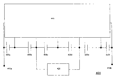
[0050] Although Figures 1-3 illustrate voltage balancer as separate devices,
this is not
a requirement of the invention. Indeed, multiple balancers can be
advantageously built as
a single device. Figure 4 illustrates a combination 400 of a stack of energy
storage cells
405, a multi-cell voltage balancer 415, and a voltage monitoring circuit 420.
[0051] This document describes in some detail inventive circuits and methods
for
monitoring voltages of stacks of cells connected in series. This was done for
illustration
purposes. Neither the specific embodiments of the invention as a whole, nor
those of its
features limit the general principles underlying the invention. In particular,
the invention
is not limited to the specific circuits and/or components described, and/or
applications
thereof. The specific features described herein may be used in some
embodiments, but
not in others, without departure from the spirit and scope of the invention as
set forth.
Many additional modifications are intended in the foregoing disclosure, and it
will be
appreciated by those of ordinary skill in the art that in some instances some
features of
the invention will be employed in the absence of a corresponding use of other
features.
The illustrative examples therefore do not define the metes and bounds of the
invention
and the legal protections afforded the invention, which function is served by
the claims
and their legal equivalents.
18