Note: Descriptions are shown in the official language in which they were submitted.
CA 02586072 2007-05-01
WO 2006/050427 PCT/US2005/039645
WIRELESS SYNCHRONOUS TIME SYSTEM
RELATED APPLICATIONS
[0001] The present patent application is a continuation-in-part of U.S. Patent
Application Serial No. 09/960,63 8, filed on September 21, 2001, now U.S.
Patent
No. 6,873,573, issued March 29, 2005, and Serial No. 10/876,767, filed on June
25,
2004, the entire contents of which are hereby incorporated by reference.
BACKGROUND OF THE INVENTION
[0002] The present invention relates to synchronous time systems and
particularly
to systems having "slave" devices synchronized by signals transmitted by a
controlling "master" device. More particularly, the present invention relates
to
synchronous time systems, wherein the master device wirelessly transmits the
signals
to the slave devices.
[0003] Conventional hard-wired synchronous time systems (e.g., clock systems,
bell systems, etc.) are typically used in schools and industrial facilities.
The devices
in these systems are wired together to create a synchronized system. Because
of the
extensive wiring required in such systems, installation and maintenance costs
may be
high.
SUMMARY OF THE INVENTION
[00041 Conventional wireless synchronous time systems are not hard-wired, but
instead rely on wireless communication among devices to synchronize the
system.
For example, one such system utilizes a government WWVB radio time signal to
synchronize a system of clocks. This type of radio controlled clock system
typically
includes a master unit that broadcasts a government WWVB radio time signal and
a
plurality of slave clocks that receive the time signal. To properly
synchronize, the
slave clock units must be positioned in locations where they can adequately
receive
the broadcast WWVB signal. Interference generated by power supplies, cornputer
monitors, and other electronic equipment may interfere with the reception (>f
the
signal. Additionally, the antenna of a radio controlled slave clock can be de-
tuned if
1
CA 02586072 2007-05-01
WO 2006/050427 PCT/US2005/039645
it is placed near certain metal objects, including conduit, wires, brackets,
bolts, etc.,
which may be hidden a building's walls. Wireless synchronous time systems that
provide reliable synchronization and avoid high installation and maintenance
costs
would be welcomed by users of such systems.
[0005] According to the present invention, a wireless synchronous time system
comprises a primary event device or "master" device including a first receiver
operable to receive a global positioning system ("GPS") time signal, and a
first
processor coupled to the first receiver to process the GPS time signal. The
primary
event device also includes a memory coupled to the first processor and
operable to
store a programmed instruction, including a preprogrammed time element and a
preprogrammed function element. The primary event device also includes an
internal
clock coupled to the first processor to store the time component and to
increment
relative to the stored time component thereafter to produce a first internal
time. A
transmitter is also included in the primary event device and is coupled to the
first
processor to transmit the first internal time and the programmed instruction.
[0006] The synchronized event system further includes a secondary event device
or "slave" device having a second receiver to wirelessly receive the first
internal time
and the programmed instruction, which are transmitted by the primary event
device.
The secondary event device includes a second processor coupled to the second
receiver to selectively register the programmed instruction, a second internal
clock
coupled to the processor to store the time component and to increment relative
to the
stored time component thereafter to produce a second internal time, and an
event
switch operable to execute the registered programmed instruction when the
second
internal time matches the preprogrammed time element of the programmed
instruction.
[0007] In some embodiments, the secondary event device or "slave" device may
include an analog clock, a digital clock, one or more time-controlled
switching
devices (e.g., a bell, a light, an electronic message board, a speaker, etc.),
or any other
device for which the functionality of the device is synchronized with other
devices.
In these devices, the programmed instruction includes an instruction to
display time
2
CA 02586072 2007-05-01
WO 2006/050427 PCT/US2005/039645
and/or an instruction to execute a function at a predetermined time. The
programmed
instruction is broadcast to the "slave" unit devices by the primary event
device or
"master" device. In this way, for example, the master device synchronizes the
time
displayed by a system of analog slave clocks, synchronously sounds a system of
slave
bells, synchronizes the time displayed by a system of slave digital clocks, or
synchronizes any other system of devices for which the functionality of the
devices of
the system is desired to be synchronized. In some embodiments, the master
device
transmits multiple programmed commands (a "program") to the slave devices and
the
slave devices include a processor operable to execute the multiple prograinmed
commands.
[0008] In some embodiments, these systems further include a power interrupt
module coupled to the processors to retain the internal time and the
programmed
instruction in the event of a power failure. Both the "master" primary event
device
and the "slave" secondary event device are able to detect a power failure and
store
current time information into separate memory modules.
[0009] The system is synchronized by first receiving a GPS time signal at the
master device and setting a first internal clock to the GPS time signal. The
first
internal clock is then incremented relative to the GPS time signal to produce
a first
internal time. Operational data in the form of the prograinmed instruction,
including
the preprogrammed time element and the preprogrammed function element, is then
retrieved from a memory and is wirelessly transmitted along with the first
internal
time. A second receiver at the "slave" device wirelessly receives the first
internal
time and the operational data and selectively registers it. A second internal
clock
within the "slave" device is set to the first internal time and is incremented
relative
thereto to produce a second internal time. In preferred embodiments, such as
an
analog clock, the second internal time is simply displayed. In other slave
devices,
such as a system of bells, a function is identified from the preprogrammed
function
element and is executed (e.g., bells or alarms are rung) when the second
internal time
matches the preprogrammed time element.
3
CA 02586072 2007-05-01
WO 2006/050427 PCT/US2005/039645
[0010] Additional features and advantages will become apparent to those
skilled
in the art upon consideration of the following detailed description of
preferred
embodiments exemplifying the best mode of carrying out the invention as
presently
perceived.
BRIEF DESCRIPTION OF THE DRAWINGS
[0011] Fig. 1 shows a block diagram of a wireless synchronous time system
according to the present invention including a master device which receives a
GPS
signal and broadcasts a time and programmed instruction to a system of slave
devices.
[0012] Fig. 2 shows a block diagram of the master device of Fig. 1.
[0013] Fig. 3A shows a time package structure used in the transmission of the
time element of Fig. 1.
[0014] Fig. 3B shows a function package structure used in the transmission of
the
programmed instruction element of Fig. 1.
[0015] Fig. 4 shows a block diagram of an analog clock slave device of Fig. 1.
[0016] Fig. 4a shows a clock movement box used in the setting of the slave
clock
of Fig. 4.
[0017] Fig. 4b shows a block diagram of a secondary device of Fig. 1.
[0018] Fig. 5a shows a block diagram of a slave device of Fig. 1, which
includes a
switch for controlling the functionality of the device.
[0019] Fig. 5b shows a block diagram of another slave device of Fig. 1, which
includes a switch for controlling the functionality of the device.
[0020] Fig. 6 shows a flow chart illustrating the functionality of a wireless
synchronous time system in accordance with the present invention.
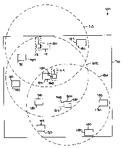
[0021] Fig. 7 shows a schematic diagram of a wireless synchronous time keeping
system.
4
CA 02586072 2007-05-01
WO 2006/050427 PCT/US2005/039645
[0022] Fig. 8 shows another schematic diagram of a wireless synchronous time
keeping system.
[0023] Fig. 9 shows a block diagram of a repeating device for use in a
wireless
synchronous time keeping system, such as the systems illustrated in Figs. 7
and 8.
[0024] Fig. 10 shows another block diagram of a repeating device for use in a
wireless synchronous time keeping system, such as the systems illustrated in
Figs. 7
and 8.
DETAILED DESCRIPTION OF THE DRAWINGS
[0025] Before any embodiments of the invention are explained in detail, it is
to be
understood that the invention is not limited in its application to the details
of
construction and the arrangement of components set forth in the following
description
or illustrated in the following drawings. The invention is capable of other
constructions and of being practiced or of being carried out in various ways.
Also, it
is to be understood that the phraseology and terminology used herein is for
the
purpose of description and should not be regarded as limiting. The use of
"including," "comprising," or "having" and variations thereof herein is meant
to
encompass the items listed thereafter and equivalents thereof as well as
additional
items. The terms "mounted," "connected," and "coupled" are used broadly and
encompass both direct and indirect mounting, connecting and coupling. Further,
"connected" and "coupled'" are not restricted to physical or mechanical
connections or
couplings and can include electrical connections and couplings, whether direct
or
indirect.
[0026] Referring to Fig. 1, a wireless synchronous time system 100 in
accordance
with the present invention includes a primary "master" device 110, which
receives a
first time signal through a receiving unit 115 and broadcasts a second time
signal to a
plurality of "slave" secondary event devices 130. The receiving unit 115 can
include
a GPS receiver 127 having an antenna 129 which receives a global positioning
system
("GPS") signal, including a GPS time signal component. The receiving unit 115
can
send the GPS time signal component to the primary master device 110 where it
is
CA 02586072 2007-05-01
WO 2006/050427 PCT/US2005/039645
processed as further discussed below. In other embodiments, the primary device
I 10
can receive a first time signal from another system that may or may not
include a GPS
time signal component.
[0027] The primary master device 110 can further include a transmission unit
120,
which wirelessly transmits a signal to the secondary or "slave" devices 130.
In one
embodiment, the signal sent to the slave devices 130 includes the processed
GPS time
signal component and/or a programmed instruction that is input to the primary
master
device I 10 through a programmer input connection 125. The programmed
instruction
includes a preprogrammed time element and a preprogrammed function element
which, along with the GPS time signal component, is transmitted by the primary
master device 110 to synchronize the slave devices 130. In one construction,
the
processed GPS time signal component and the programmed instruction are
wirelessly
transmitted to the slave devices 130 at approximately a frequency between 72
and 76
MHz. In another construction, the processed GPS time signal component and the
programmed instruction are wirelessly transmitted to the secondary devices 130
at a
frequency of approximately 154 MHz.
[0028] Fig. 1 illustrates a few examples of secondary or slave devices 130. As
shown in Fig. 1, examples of secondary or slave devices 130 can include an
analog
time display 145, a digital time display 135, and one or more switching
devices 140,
which may be associated with any one of a number of devices, such as a bell, a
light,
a lock, a speaker, etc. In other constructions, such as the construction
illustrated in
Fig. 4b, the secondary device 130 can also include such devices as a message
board
147.
[0029] Each of the secondary devices 130 includes an antenna 150 to wirelessly
receive the signal from the primary device 110, such as, for example, the
processed
GPS time signal component and the programmed instruction from the primary
master
device 110. Each of the secondary devices 130 also includes a processor (see
Fig. 4,
element 410 and Fig. 5, element 525, not shown in Fig. 1) to process the
processed
time signal and the programmed instruction received from the primary device
110. As
will be further discussed below, in some constructions, when the preprogrammed
time
6
CA 02586072 2007-05-01
WO 2006/050427 PCT/US2005/039645
element of the programmed instruction matches a second time generated by the
slave
device, an event will be executed.
[0030] The primary device 110 may also transmit one or more programmed
instructions (a "program") that may be executed by the processor of the
secondary
devices 130. The program may include a message to be displayed by a message
board, a tone or wave file (a "sound file") to be generated by a speaker, an
image file
to be displayed by a monitor, or a function or algorithm to be performed on a
data set.
The secondary devices 130 may also store one or more programs in an internal
memory and simply receive a direction of which program to retrieve from the
internal
memory and execute from the primary device 110. The primary device 110 may
also
transmit input parameters to the secondary devices 130 that the processor may
use
when executing a program.
[0031] For the analog time display 145, shown in Fig. 1, the event can include
positioning an hour, minute, and second hand to visually display the current
time. For
the digital time display 145, the event can include digitally displaying the
current
time. For a time controlled switching device 140, the event may include any of
a
number of events that may be controlled by the switch. For example, a system
of
bells may include switches that sound the bells at a particular time.
Alternatively, a
system of lights may include switches which turn the lights on or off at a
particular
time. For the message board 147 (see Fig. 4b), in one construction, the event
may
include displaying a message stored in the board's memory at a certain time.
In
another construction, for the message board 147, the event may include
displaying a
message that accompanies the time component.
[0032] It will be readily apparent to those of ordinary skill in the art that
the
secondary devices may include any one of a number of electronic devices for
which a
particular functionality is desired to be performed at a particular time, such
as
televisions, radios, electric door locks, lights, etc.
[0033] Referring to Fig. 2, a detailed diagram of the primary master device
110 is
shown. The primary master device 110 can receive a time signal component, such
as
7
CA 02586072 2007-05-01
WO 2006/050427 PCT/US2005/039645
the GPS time signal component from the receiving unit 115 (Fig. 1) at an input
unit,
such as the GPS time signal input receiving unit or connector 205. The primary
master device 110 can further include a processor 210, a memory 215, a
programmer
input connector 125, a communication port 220, a display 225, a transmission
unit
120, and a powered input socket 235. In some embodiments, these elements of
the
primary master device 110 serve to receive, process, and transmit information
used to
synchronize the slave units 130, as will be fully discussed below. The
communication
port 220 may be used to perform diagnostic testing or auditing or to perform
software
upgrades or modifications by an external computing device (i.e., a personal
computer,
a PDA, etc.). Additionally, a channel switch 245, time zone switch 250, and a
daylight savings bypass switch 255 can be included in the primary master
device 110.
Lastly, in some embodiments, the primary master device 110 includes a power
interrupt module 258 coupled to the processor 210 to retain the internal time
and the
programmed instruction in the event of a power loss.
[0034] In some embodiments, upon powering up the master device 110, the
processor 210 can check the setting of the channel switch 245, the time zone
switch
250, and the daylight savings bypass switch 255. The processor 210 stores the
switch
information into the memory 215. In some embodiments, a signal is received
through
the antenna 129 and a time signal component is extracted from it. For example,
in
some embodiments using a GPS time signal, a GPS signal is received through the
antenna 129 and a GPS time signal component is extracted from it. When the
receiving unit or connector 205 receives the GPS time signal component, the
processor 210 adjusts it according to the switch information of the channel
switch
245, the time zone switch 250, and the daylight savings bypass switch 255, and
sets
an internal clock 260 to the processed GPS time signal component to produce a
first
internal time.
[0035] The channel switch 245 enables a user to select a particular
transmission
frequency or range of frequencies determined best for transmission in the
usage area,
and to independently operate additional primary master devices in overlapping
broadcast areas without causing interference between them. The GPS time signal
uses a coordinated universal time ("UTC"), and requires a particular number of
8
CA 02586072 2007-05-01
WO 2006/050427 PCT/US2005/039645
compensation hours to display the correct time and date for the desired time
zone.
The time zone switch 250 enables the user to select a desired time zone, which
permits worldwide usage. The time zone switch 250 or a separate switch may
also be
used to compensate for fraction-of-an-hour time differences. For example, in
some
areas a half-an-hour time offset may be added to the received time component
to
generate a correct time. Lastly, the GPS time signal may or may not include
daylight
savings time information. As a result, users in areas that do not require
daylight
savings adjustment may be required to set the daylight savings bypass switch
255 to
bypass an automatic daylight savings adjustment program. Manual daylight
savings
time adjustment can also be accomplished by adjusting the time zone switch 250
to a
desired time zone retain a correct time.
[0036] Once the processor 210 adjusts the GPS time signal component according
to the settings of the switches discussed above and sets the internal clock
260 to
produce the first internal time, the internal clock 260 starts to increment
the first
internal time until another GPS time signal is received from the GPS receiver
127
(Fig. 1). Between receiving GPS time signals, the internal clock 260
independently
keeps the first internal time which, in addition to date information and
reception
status, is displayed on the display 225. The internal clock 260 may also
include a
back-up power source 270 for retaining power to the internal clock if a
primary povver
source (i.e., power supplied by an alternating current outlet) is lost,
disrupted, or
insufficient for supplying needed power to the master device 110. In some
embodiments, the back-up power source 270 includes a battery. In addition to
processing the time signal, the processor 210 also checks for a new programmed
instruction on a continuous basis, and stores any new programmed instruction
in the
memory 215. As briefly mentioned above, to enter a programmed instruction, a
user
keys in the programmed instruction into a computing device (e.g., a personal
computer, a PDA, etc.) and transfers the programmed instruction to the primary
master device 110 through the programmer input connector 125. The programmed
instruction is stored in the memory 215 and, along with the first internal
time kept in
the internal clock 260, is transmitted through the transmission unit 120 at
the
transmission frequency set in the channel switch 245.
9
CA 02586072 2007-05-01
WO 2006/050427 PCT/US2005/039645
[0037] The first internal time and the programmed instruction are transmitted
by
the master device 110 using a data protocol as shown in Figs. 3A and 3B. Fig.
3A
shows a time packet structure 300 comprising of preprogrammed time element,
and
having a 10-bit preamble 304, a sync bit 308, a packet identity byte 312, an
hour byte
316, a minute byte 320, a second byte 324, a checksum byte 328 and a postamble
bit
332. Fig. 3B shows a function packet structure 350 comprising a preprogrammed
function element, and having a 10-bit preamble 354, a sync bit 358, a packet
identity
byte 362, an hour byte 366, a minute byte 370, a function byte 374, a checksum
byte
378, and a postamble bit 382.
[0038] Each secondary slave device 130 receives the signal broadcast by the
master device 110 including information according to the time packet structure
of Fig.
3A and the function packet structure Fig. 3B. The secondary slave device
attempts to
match the packet identity bytes 312 or 362 with an internal identity number
programmed in the processor of the secondary slave device (i.e., 410 of Fig. 4
or 525
of Fig. 5) to selectively register the program instruction. It should be
readily apparent
to those of ordinary skill in the art that the time packet structure 300 and
the function
packet structure 350 may have a different structure size so that more or less
information may be transmitted using these packets. For example, the time
packet
structure may include, in addition to the existing timing bytes, a month byte,
a day
byte, a year byte, and a day of the week byte. Similarly, the function packet
structure
350 may include additional hour, minute, and function bytes to terminate the
execution of an event triggered by the hour, minute, and function bytes 366,
370, and
374, shown in Fig. 3B.
[0039] A diagram of the analog slave clock 145 of Fig. 1 is shown in Fig. 4.
The
slave clock 145 includes a second receiving unit 402 having an antenna 150 and
a
second receiver 406. The slave clock 145 also includes a second processor 410,
a
second memory 415, a second internal clock 420 and an analog display 425. The
analog display 425 includes a set of hands 430 including a second hand 432, a
minute
hand 434, and an hour hand 436. As with the master device 110, the secondary
slave
clock 145 also includes a power interrupt module 438 coupled to the processor
410 to
CA 02586072 2007-05-01
WO 2006/050427 PCT/US2005/039645
retain an internal time and a programmed instruction in the event of a power
loss to
the slave clock 145.
[0040] In some constructions, the secondary devices 130 can also include an
indicator 417 that indicates whether the secondary device 130 is receiving any
signals
from the primary device 110. In one construction, the indicator 417 can
include a
light emitting diode ("LED") that flashes in response to every incoming signal
received and processed by the secondary device 130. In another construction,
the
indicator 417 can include an LED that flashes after a certain period of time
elapses
during which the secondary device 130 does not receive any signal from the
primary
device 110. In other constructions, the indicator 417 can include a speaker
operable
to indicate the reception or lack of reception of a signal with an audible
indication.
[0041] In some constructions, the indicator 417 can also be used to indicate
the
execution of an instruction. For example, an LED may flash or a speaker may
transmit a sound or recording that indicates that an event will occur, is
occurring, or
has occurred, such as the locking of a door or the turning off of a light.
[0042] In some constructions, the secondary devices 130 also include a power
source 418. In the illustrated construction of Fig. 4, the power source 418
includes a
battery, such as a D-size battery, for example. The second devices 130 may
also
include a solar panel or other generally portable power source. In these
constructions,
the secondary devices 130 do not need to be placed within an area with a power
source readily available, such as, for example, within a certain area of an
alternating
current ("AC") outlet that can have a generally fixed position that limits the
placement of the secondary device 130. In some constructions, the primary
device
110 may include a generally portable power source such as battery or solar
panel.
[0043] Fig. 4a illustrates a clock movement box 450 having a manual time set
wheel 465, and a push button 470 for setting the position of the hands 430 of
the
analog display 425. The clock movement box 450 is of the type typically found
on
the back of conventional analog display wall clocks, and is used to set such
clocks. In
setting the analog slave clock 145, the manual time set wheel 465 of the clock
11
CA 02586072 2007-05-01
WO 2006/050427 PCT/US2005/039645
movement box 450 is initially turned until the set of hands 430 shows a time
within
29 minutes of the GPS time (i.e., the actual time). When power is applied to
the slave
analog clock 145, the second hand 432 starts to step. The push button 470 of
the
clock movement box 450 is depressed when the second hand reaches the 12
o'clock
position. This signals to the second processor 410 that the second hand 432 is
at the
12 o'clock position, enabling the second processor 410 to "know" the location
of the
second hand 432. The push button 470 is again depressed when the second hand
432
crosses over the minute hand 434, wherever it may be. This enables the second
processor 410 to "know" the location of the minute hand 434 on the clock dial.
(See
U.S. Patent Application No. 09/645,974 to O'Neill, the disclosure of which is
incorporated by reference herein). The second processor 410 may also "know"
the
location of the hands of the clock dial by optically detecting the position of
gears
within the clock that determine the position of the hands or the hands
themselves.
[0044] To synchronize itself to the master device 110, the second receiver 406
of
the slave device 145 automatically and continuously or periodically searches a
transmission frequency or a channel that contains the first internal time and
the
programmed instruction. When the receiving unit 402 wirelessly receives and
identifies the first internal time, the processor 410 stores the received
first internal
time at the second internal clock 420. The second internal clock 420
immediately
starts to increment to produce a second internal time. The second internal
time is kept
by the second internal clock 420 until another first internal time signal is
received by
the slave clock 145. If the processor 410 determines that the set of hands 430
displays
a lag time (i.e., since a first internal time signal was last received by the
slave clock
145, the second internal clock 420 had fallen behind), the processor 410
speeds up the
second hand 432 from one step per second to a rate greater than one step per
second
until both the second hand 432 and the minute hand 434 agree with the newly
established second internal time. If the processor 410 determines that the set
of hands
430 shows a lead time (i.e., since the first internal time signal was last
received by the
slave clock 145, the second internal clock 420 had moved faster than the time
signal
relayed by the master device), the processor 410 slows down the second hand
432
from one step per second to a rate less than one step per second until both
the second
12
CA 02586072 2007-05-01
WO 2006/050427 PCT/US2005/039645
hand 432 and the minute hand 434 agree with the newly established second
internal
time.
[0045] Fig. 4b illustrates a message board 147, which is another example of a
secondary device 130 for use in the synchronous system 100. In some
constructions,
the message board 147 includes similar components to the slave clock 145, such
as,
for example, a receiving unit 402, a processor 410, memory 415, a power
interrupt
module 438, and an internal clock 420. The message board 147 further includes
a
display 421. In some constructions, the message board 147 can store
preprogrammed
messages in a portion 415a of memory 415. The messages can be hardwired into
the
memory portion 415a or can be manually entered via a programmer input
connector
416. In other constructions, the messages are stored in the primary device 110
and are
wirelessly transmitted to the board 147. In these constructions, the processor
410 can
parse the signal, extract the message and the time at which the message is to
be
displayed, and store that information in memory 415. In furtlier
constructions, the
message board 147 can also include an analog clock movement unit (not shown)
to
display time or can show the time on the display 421.
[0046] In addition to slave clocks that display the synchronized time signal,
a
slave device 130 may include one or more switching slave devices 140 as
depicted in
Figs. 5a and 5b. Instead of simply displaying a time signal, the switching
slave device
140 utilizes a time signal to execute an event at a particular time, such as
displaying a
message on a message board, for example. In this way, a system of slave
switching
devices can be synchronized.
[0047] The slave switching device 140 includes a second receiving unit 510
having an antenna 150 and a second receiver 520, a second processor 525, a
second
internal clock 530, a second memory 535, an operating switch 540, and a device
power source 550. The secondary slave switching device 140 further includes a
power interrupt module 552 coupled to the processor 410 to retain the internal
time
and the programmed instruction on a continuous basis, similar to the power
interrupt
module of the master device 110 and the slave clock 145. The secondary slave
switching device 140 includes any one of a number of devices 555, which is to
be
13
CA 02586072 2007-05-01
WO 2006/050427 PCT/US2005/039645
synchronously controlled. Depending upon the device 555 to be controlled, a
first
end 560 of the device 555 is coupled to a normally open end ("NO") 565 or a
normally closed end ("NC") 570 of the operating switch 540. The first power
lead
575 of the device power source 550 is also coupled to a second end 580 of the
device
555, and a second power lead 585 of the device power source 550 is configured
to be
coupled to the normally open end 565 or the normally closed end 570 of the
operating
switch 540. The operating switch 540 may close and/or open a connection
between
the second power lead 585 and the normally open end 565 or normally closed end
570
of the operating switch 540 to break or complete a circuit that provides
operating
power or instructions to the device 555. It will be readily apparent to those
of
ordinary skill in the art that the device 555 and operating switch 540 may be
constructed and operated in other constructions and/or manners than those
illustrated
and described. For example, the operating switch 540 may generate and transmit
operating power and/or instructions over a wireless connection, such as over a
radio
frequency or infrared signal, to the device 555. The device 555 receives the
operating power and/or instructions and begins and/or stops operating or
modifies its
operation as instructed.
[0048] As shown in Fig. 5b, the switching device 140 can also include one or
more sensors 590. In some constructions, the sensor(s) 590 provides feedback
regarding a performed event. For example, once an event is executed, such as
closing
and locking a door at a certain time, the sensor(s) 590 can verify whether the
event
was performed.
[0049] In other constructions, the sensor(s) 590 can provide an additional
input
factor for determining whether an event should take place. For example, the
sensor
590 can include one or more motion detectors and an event can include turning
off
overhead lights at a certain time. If the motion detector(s), however, detects
someone
within a specified proximity, the processor 525 can determine not to execute
the event
(e.g., turn off the lights) at the scheduled time. Furthermore, feedback from
the
sensor(s) 590 can provide additional functionality, such as providing
announcement
of the execution of an event or enabling a warning once an event has been
executed.
For example, a buzzer or recording via a speaker can sound prior to an event,
such as
14
CA 02586072 2007-05-01
WO 2006/050427 PCT/US2005/039645
closing and locking a door. Also, the buzzer or recording can sound if someone
attempts to open a door after a certain time.
[0050] Still referring to Fig. 5b, the secondary devices 130 can also record
information from the one or more sensors 590 in memory 535. In some
constructions,
the devices 130 may include additional non-volatile memory. The secondary
device
130 can also maintain a record of its operation in memory 535.
[0051] In some constructions, the memory 535 can also store time adjustment
information such as daylight savings information, time zone information, etc.
The
time adjustment information can serve as a back-up in the event the secondary
device
130 does not receive a signal from the primary device 110 or receives a signal
from
the primary device 110 that requires additional time adjusting than that
performed by
the primary device 110. For example, a group of secondary devices 130 may
receive
identical signal from a primary device 110, but one of the secondary devices
130 may
process the received signal to display the time in one time zone (i.e., the
time in New
York) and another secondary device 130 may process the received signal to
display
the time in another time zone (i.e., the time in Paris).
[0052] In some constructions, the system 100 also allows for two-way
communication between secondary devices 130 and primary device 110. In these
constructions, the secondary device 130 can include a transceiving unit 592
(see Fig.
5b) in place of the second receiving unit 402 or can include both the second
receiving
unit 402 and a second transmitting unit (not shown). In these constructions,
signals
are transmitted at a frequency of approximately 154 MHz between the primary
device
110 and the secondary device 130. The transceiving unit 592 may be operable to
receive a second signal from the primary device 110 and transmit a third
signal to the
primary device 110.
[0053] In some constructions, like the receiver;406 of the slave clock 145,
the
second receiver 520 of the slave switching device 140 automatically searches a
transmission frequency or a channel that contains a first internal time and a
programmed instruction from the master device 110. When the receiving unit 510
CA 02586072 2007-05-01
WO 2006/050427 PCT/US2005/039645
wirelessly receives and identifies the first internal time, the second
processor 525
stores the received first internal time in a second internal clock 530. The
second
internal clock 530 immediately starts to increment to produce a second
internal time
until another first internal time signal is received from the master device
110.
[0054] Additionally, in some constructions, the programmed instruction can be
stored in the memory 535. When there is a match between the second internal
time
and the preprogrammed time element of the programmed instruction, the
preprogrammed function element will be executed. For example, if the
preprogrammed time element contains a time of day, and the preprogrammed
functional element contains an instruction to switch on a light, the light
will be
switched on when the second internal clock 530 reaches that time specified in
the
preprogrammed time element of the programmed instruction.
[0055] In other constructions, the switching device 140 does not store
programmed instructions in memory 535. Rather, switching device 140 may
receive
instructions from the signal received from the primary device 110.
[0056] Referring to Fig. 6, a flow chart 600 illustrates a wireless
synchronous
time system according to the present invention. The flow chart 600 illustrates
the
steps performed by a wireless synchronous time system according to the present
invention for any number of systems of slave devices. The process starts in a
receiving step 610 where a master device receives a GPS time signal. As
indicated in
the flow chart at step 610, the master device will continuously look for and
receive
new GPS time signals. Next, at step 615, a first internal clock is set to the
received
GPS time. Next, the first internal clock will start to increment a first
internal time in
step 620. In a parallel path, at step 625, the master device receives
programmed
instructions input by a user of the system. Again, the flow chart indicates
that the
master device is able to continuously receive programmed instructions so that
a user
may add additional programmed instructions to the system at any time. As
discussed
above, the programmed instructions will include a preprogrammed time element
and a
preprogrammed function element. The programmed instruction is then stored in a
first memory at step 627. Next, when preset periodic times are reached at step
629,
16
CA 02586072 2007-05-01
WO 2006/050427 PCT/US2005/039645
the programmed instruction is retrieved at step 630 and transmitted at step
632 to the
slave device along with the first internal time at step 63 5. In other words,
when the
first internal clock reaches particular preset times (e.g., every five
minutes) the
programmed instruction and the first internal time are wirelessly transmitted
to the
slave devices. The intermittent transmissions may conserve power consumption
of
the master device and slave devices, since the frequency of wireless
transmission can
be regulated such that the devices operate with low power consumption.
[0057] The programmed instruction and/or the first internal time are received
at
the slave device in step 640. If the slave device is to merely synchronously
display a
time, such as a clock, but does not perform any functionality, there is no
need to
receive a programmed instruction. In slave devices such as bells, lights,
locks, etc., in
addition to the first internal time, at step 642, the processor will select
those
programmed instructions where the packet identity byte matches an identity of
the
slave device. The selected programmed instruction is then stored or registered
in
memory at the secondary slave device in step 645. A second internal clock is
then set
to the first internal time at step 650 to produce a second internal time. In
step 655,
like the first internal clock, the second internal clock will start to
increment the second
internal time. The second internal time is displayed at step 665. Meanwhile, a
function is identified from the preprogrammed function element at step 670.
When
the second internal time has incremented to match the preprogrammed time
element at
step 675, the function identified from the preprogrammed function element is
executed in step 680. Otherwise, the secondary slave device will continue to
compare
the second internal time with the preprogrammed time element until a match is
identified.
[0058] It will be readily understood by those of ordinary skill in the art,
that both
the first internal clock and the second internal clock increment, and thus
keep a
relatively current time, independently. Therefore, if, for some reason, the
master
device does not receive an updated GPS time signal, it will still be able to
transmit the
first internal time. Similarly, if, for some reason, the slave device does not
receive a
signal from the master device, the second internal clock will still maintain a
relatively
current time. In this way, the slave device will still display a relatively
current time
17
CA 02586072 2007-05-01
WO 2006/050427 PCT/US2005/039645
and/or execute a particular function at a relatively accurate time even if the
wireless
communication with the master device is interrupted. Additionally, the master
device
will broadcast a relatively current time and a relatively current programmed
instruction even if the wireless communication with a satellite broadcasting
the GPS
signal is interrupted. Furthermore, the power interrupt modules of the master
and
slave devices help keep the system relatively synchronized in the event of
power
interruption to the slave and/or master devices.
[0059] In some constructions and in some aspects, the wireless synchronous
time
system 100 can include a primary device, one or more secondary devices, and
one or
more repeating devices. In some constructions, the primary device refers to
the
device that receives an initial reference time signal from a source, such as,
for
example, a source external to the system 100 (e.g., a GPS time signal from a
GPS
satellite). In these constructions, the repeating devices can be used to
extend the
coverage area of the system 100. 1
[0060] For example, in the embodiment illustrated in Fig. 7, the system 100
can
be used to synchronize certain devices within a desired area 710. In some
constructions, for example, the area 710 can include a building, such as an
office
building, a school, a department store, a hospital, a hotel, or the like. In
other
constructions, for example, the area 710 can include multiple buildings, such
as a
campus.
[0061] As shown in Fig. 7, the system 100 includes a primary device 110. In
the
illustrated embodiment, the primary device 110 is coupled to a receiving unit
115. In
some constructions, the receiving unit 115 can receive a GPS time signal or
another
signal with a time component. In other constructions, the receiving unit 115
can
receive a terrestrial signal. In further constructions, the receiving unit 115
can receive
another satellite signal.
[0062] In the illustrated embodiment, the primary device 110 further includes
a
transmitting unit 120. The transmitting unit 120 can wirelessly transmit a
signal
across a first coverage area 715 to one or more secondary devices 130. As
shown in
18
CA 02586072 2007-05-01
WO 2006/050427 PCT/US2005/039645
Fig. 7, the primary device 110 can transmit signals to a first secondary
device 720 and
a second secondary device 725, both of which are included in the first
coverage area
715. In other constructions, the system 100 can include more or fewer
secondary
devices 130 within the first coverage area 715 of the primary device 1 10.
[0063] In the illustrated embodiment, the area 710 in which the system 100
operates within is larger than the first coverage area 715 of the primary
device 110.
Furthermore, the system 100 also includes additional secondary devices 130
that are
not positioned within the first coverage area 715 of the primary device 110,
such as,
for example, a third secondary device 730, a fourth secondary device 740, a
fifth
secondary device 745, a sixth secondary device 750, and a seventh secondary
device
755. In some constructions, such as the illustrated embodiment, these
additional
secondary devices 130 receive signals from the primary device 110 vi a one or
more
repeating devices 800.
[0064] As shown in Fig. 7, for example, the third secondary device 730 and the
fourth secondary device 740 receive signals from the primary device 110 via a
first
repeating device 810. In this embodiment, the first repeating device g 10 is
positioned
within the first coverage area 715 of the primary device 110 and is equipped
to
receive signals transmitted from the primary device 110. Furthermore, in some
constructions, the first repeating device 810 can be equipped to retransmit
the signals
to secondary devices 130 within a second coverage area 812. As shovvn in Fig.
7, the
third secondary device 730 and the fourth secondary device 740 are positioned
within
the second coverage area 812 of the first repeating device 810 and outside the
first
coverage area 715 of the primary device 110.
[0065] Also shown in Fig. 7, the fifth secondary device 745, the sixth
secondary
device 750 and the seventh secondary device 755 are each positioned outside
both the
first coverage area 715 of the primary device 110 and the second coverage area
812 of
the first repeating device 810. In the illustrated embodiment, these secondary
devices
130 receive the signals from the primary device 110 via a second repeating
device 815
transmitting within a third coverage area 816. As shown in Fig. 7, the second
repeating device 815 is positioned within the second coverage area 812 of the
first
19
CA 02586072 2007-05-01
WO 2006/050427 PCT/US2005/039645
repeating device 810 and outside the first coverage area 715 of the primary
device
110.
[0066] Another example of the location of the devices within the system is
shown
in Fig. 8. In this construction, for example, each repeating device 800 can be
located
within the first coverage area 715 of the primary device 110.
[0067] In some constructions, the overlapping regions of the coverage area of
the
primary device 110 (such as, for example, the first coverage area 715) and the
coverage area of the repeating device 800 (such as, for example, the second
coverage
area 812) can vary for different applications. For example, the system 100 can
be
used to synchronize various devices 130 within a multi-story building. Even
though
the primary device 110 may be able to transmit throughout the entire building,
repeating devices 800 can be included in order to strengthen the signals from
the
primary device 110.
[0068] In some constructions, as mentioned previously, the repeating devices
80
can be equipped to retransmit the signals received from the primary device 110
to
secondary devices 130 within a particular coverage area. In other
constructions, the
repeating devices 800 can be equipped to process the signals transmitted by
the
primary device 110 and transmit processed signals or different signals to the
secondary devices 130 within the particular coverage area. For example, the
signal
sent by the primary device 110 (e.g., the primary signal) may include a time
and an
instruction. In some constructions, a repeating device 800, such as the first
repeating
device 810, can process the signal and extract the time information and the
instruction. Furthermore, the repeating device 800 can be equipped to modify
the
instruction, remove the instruction, and/or replace the instruction with a
second
instruction. Also, in some constructions, the repeating device 800 can modify
the
time information included in the primary signal and transmit updated time
information to the secondary devices 130. In these constructions, the
repeating device
110 can modify the time to reflect instances of daylight savings or time zone
changes,
for example.
CA 02586072 2007-05-01
WO 2006/050427 PCT/US2005/039645
[0069] In further constructions, the repeating devices 800 can receive a
second
signal from the primary device 110 on a first frequency. For example, the
second
signal can include a time and an instruction. A repeating device 800 can
receive the
second signal, process the second signal and transmit a third signal at a
second
frequency to another device such as another repeating device 800 or a
secondary
device 130. The third signal can include the time and the instruction from the
second
signal or can include one of a modified time and a modified instruction. In
some
constructions, the first frequency and the second frequency may be the same
frequency. The first frequency and the second frequency may also be different
frequencies.
[0070] Figs. 9 and 10 illustrate examples of repeating devices 800 for use in
the
wireless system 100. In some constructions, such as the constructions
illustrated in
Figs. 7, 8 and 9, the repeating device 800 can include components similar to
the
primary device 110. As shown the illustrated constructions, the repeating
device 800,
such as the first repeating device 810, can include an input connector 906
coupling it
to an external receiving unit 905. In other constructions, such as the
construction
shown in Fig. 10, the repeating device 800, such as the second repeating
device 815
(shown in Figs. 7 and 8) can include an internal receiving unit 908.
[0071] Similar to the primary device 110, the repeating device 800 can include
processor 910, memory 915, a transmission unit 920, a display 925, a
programmer
input connector 930, a power input socket 935, a channel switch 945, a time
zone
switch 950, a daylight savings bypass switch 955, a power failure module 958,
and an
internal clock 960. In some coristructions, the repeating device 800 includes
fewer
modules than shown and described in Figs. 9 and 10. In other constructions,
the
repeating device 800 includes additional modules. In further constructions,
the
repeating device 800 includes fewer modules than the primary device 110. For
example, in one construction, the repeating device 800 may only include an
internal
receiving unit 906, a processor 910, a memory 915, a transmission unit 920,
and an
internal clock 960. In still fiuther constructions, the repeating device 800
includes
more modules than the primary device 110.
21
CA 02586072 2007-05-01
WO 2006/050427 PCT/US2005/039645
[0072] In other constructions, the repeating device 800 may receive an initial
reference time signal from an external source, such as a GPS satellite, and
may
transmit the received time signal to the primary device. For example, the
repeating
device 800 may be placed outdoors or in another environment that provides a
clear
and generally unobstructed path for the reception of an initial reference or
first signal
with a first time component. Upon receiving the first signal, the repeating
device 800
may process the first signal, as described above, to produce a second time
component.
For example, the repeating device 800 may modify the first time component to
account for daylight savings or time zones. The repeating device 800 may also
transmit the time component of the first signal without processing it. The
repeating
device 800 transmits a second signal to the primary device 110 that includes
the
second time component. In some constructions, the repeating device 800 may
receive
the first signal on a first frequency and may transmit the second signal to
the primary
device 110 on a second frequency. The second frequency may be a lower
frequency
that has better material penetration than the first frequency.
[0073] Upon receiving the second signal, the primary device 110 may operate as
previously described for systems without a repeating device 800. In some
constructions, the primary device 110 processes the second signal to produce a
third
time component and transmits the third time component and a programmed
instruction and/or event in a third signal to a secondary device 130. The
primary
device 110 may also transmit the third signal to a repeating device 800.
[0074] It is to be understood that the invention is not limited in its
application to
the details of construction and the arrangement of components set forth in the
above
description or illustrated in the drawings. The invention is capable of other
embodiments and of being practiced or being carried out in various ways. Also,
it is
to be understood that the phraseology and terminology used herein is for the
purpose
of description and should not be regarded as limited. The use of "including"
and
"comprising" and variations thereof herein is meant to encompass the items
listed
thereafter in accordance thereof as well as additional items. Although the
invention
has been described in detail with reference to certain embodiments, variations
and
22
CA 02586072 2007-05-01
WO 2006/050427 PCT/US2005/039645
modifications exist within the scope and spirit of the invention as described
and
defined in the following claims.
23