Note: Descriptions are shown in the official language in which they were submitted.
CA 02587437 2010-10-29
PU040322
1
METHODS, APPARATUS AND SYSTEM FOR FILM GRAIN CACHE SPLITTING
FOR FILM GRAIN SIMULATION
FIELD OF THE INVENTION
The present invention generally relates to film grain simulation and, more
particularly, to methods and system for efficient, low-cost film grain
simulation
implementations.
BACKGROUND OF THE INVENTION
Film grain forms in motion picture images during the process of
development. Film grain is clearly noticeable in HD images and becomes a
distinctive cinema trait that is becoming more desirable to preserve through
the
whole image processing and delivery chain. Nevertheless, film grain
preservation
is a challenge for current encoders since compression gains related to
temporal
prediction cannot be exploited. Because of the random nature of the grain,
visually
lossless encoding is only achieved at very high bit-rates. Lossy encoders tend
to
suppress the film grain when filtering the high frequencies typically
associated with
noise and fine textures.
In the recently created H.264 I MPEG-4 AVC video compression standard,
and in particular in its Fidelity Range Extensions (FRExt) Amendment 1 (JVT-
K051, ITU-T Recommendation H.264 I ISO/IEC 14496-10 International Standard
with Amendment 1 , Redmond, USA, June 2004), a film grain Supplemental
Enhancement Information (SEI) message has been defined. Such a message
describes the film grain characteristics regarding attributes like size and
intensity,
and allows a video decoder to simulate the film grain look onto a decoded
picture.
The H.264 I MPEG-4 AVC standard specifies which parameters are present in the
CA 02587437 2007-05-11
WO 2006/057937
PCT/US2005/042046
2
film grain SEI message, how to interpret them and the syntax to be used to
encode the SEI message in binary format. The standard does not specify,
however, the exact procedure to simulate film grain upon reception of the film
grain SEI message.
Film grain simulation is a relatively new technology used in post-production
to simulate film grain on computer-generated material, as well as during
restoration of old film stocks. For this kind of applications, there exists
commercial
software in the market like Cineon , from Eastman Kodak Co, Rochester, NY,
and Grain SurgeryTM, from Visual Infinity. These tools require user
interaction and
are complex to implement, which makes them unsuitable for real-time video
coding applications. Furthermore, none of these tools has the capability to
interpret a film grain SEI message as specified by the H.264 / AVC video
coding
standard.
SUMMARY OF THE INVENTION
The present invention provides a method, apparatus and system for film
grain cache splitting for film grain simulation.
In one embodiment of the present invention a method for storing film grain
patterns includes storing at least a first portion of film grain patterns in
an internal
memory and storing at least a second portion of the film grain patterns in an
external memory.
In an alternate embodiment of the present invention an apparatus for film
grain simulation includes a means for receiving at least an encoded image and
supplemental information including film grain characterization information for
use
in a film grain simulation process, an internal storage means for storing at
least a
first portion of film grain patterns, and an external storage means for
storing at
least a second portion of the film grain simulation patterns.
In an alternate embodiment of the present invention a system for simulating
film grain includes a decoder for receiving at least an encoded image and a
supplemental information message including film grain characterization
information for use in a film grain simulation process, an internal storage
means
for storing at least at least a first portion of film grain patterns, and an
external
CA 02587437 2007-05-11
WO 2006/057937
PCT/US2005/042046
3
storage means for storing at least a second portion of the film grain
simulation
patterns, wherein the internal storage means is located in the decoder.
BRIEF DESCRIPTION OF THE DRAWINGS
The teachings of the present invention can be readily understood by
considering the following detailed description in conjunction with the
accompanying drawings, in which:
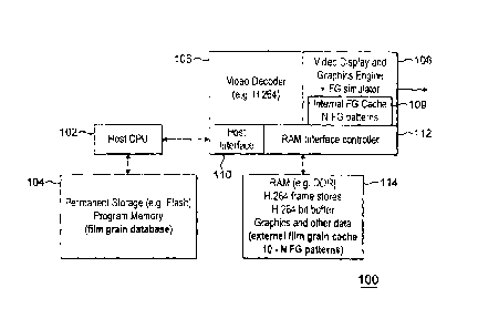
FIG. 1 depicts a high level block diagram of a video decoder subsystem
having film grain simulation capabilities in accordance with one embodiment of
the
present invention; and
FIG. 2 depicts a high level block diagram of a typical arrangement of the
film grain database of FIG. 1.
It should be understood that the drawings are for purposes of illustrating
the concepts of the invention and are not necessarily the only possible
configuration for illustrating the invention. To facilitate understanding,
identical
reference numerals have been used, where possible, to designate identical
elements that are common to the figures.
DETAILED DESCRIPTION OF THE INVENTION
The present invention advantageously provides methods, apparatuses and
systems for film grain cache splitting for film grain simulation. Although the
present invention will be described primarily within the context of a video
decoder
subsystem for application in, for example, IC designs for consumer HD DVD
players, the specific embodiments of the present invention should not be
treated
as limiting the scope of the invention. It will be appreciated by those
skilled in the
art and informed by the teachings of the present invention that the concepts
of the
present invention can be advantageously applied in any film grain simulation
processes in, for example, media player/receiver devices, decoders, set-top
boxes, television sets or the like.
FIG. 1 depicts a high level block diagram of a video decoder subsystem
having film grain simulation capabilities in accordance with one embodiment of
the
CA 02587437 2007-05-11
WO 2006/057937
PCT/US2005/042046
4
present invention. The video decoder subsystem 100 of FIG. 1 illustratively
comprises a video decoder (illustratively a H.264 decoder) 106, a video
display
and graphics engine and film grain simulator 108, a host interface 110, an
interface controller (illustratively a RAM interface controller) 112, and a
memory
(illustratively an external Ram memory) 114 implemented as a film grain cache
for
storing at least a small subset of the film grain patterns of the remote film
grain
database 104. The video display and graphics engine and film grain simulator
108 of FIG. 1 illustratively further comprises internal storage capabilities
illustratively depicted as internal film grain cache 109. Although in FIG. 1,
the
internal film grain cache 109 is depicted as being located in the video
display and
graphics engine and film grain simulator 108, in alternate embodiments of the
present invention, the internal film grain cache of the present invention may
be
located internal to the video decoder 106 or other components of the video
decoder subsystem 100 of FIG. 1.
FIG. 1 further depicts a host CPU 102 and a permanent storage program
memory (illustratively a remote permanent storage memory) 104 comprising a
film
grain database. Although in the video decoder subsystem 100 of FIG. 1, the
host
CPU 102 and the remote film grain database 104 are depicted as comprising
separate components, in alternate embodiments of the present invention, the
remote film grain database 104 can be located in a permanent memory of the
CPU 102. Furthermore, although in the video decoder subsystem 100 of FIG. 1,
the video decoder 106, the video display and graphics engine 108, the host
interface 100, and the interface controller 112 are depicted as comprising
separate components, in alternate embodiments of the present invention, the
video decoder 106, the video display and graphics engine 108, the host
interface
100, and the interface controller 112 can comprise a single component and can
be
integrated in a single integrated system-on-chip (SoC). In such an embodiment,
the video decoder subsystem 100 of FIG. 1 would comprise an internal on chip
film grain cache 109 and an external film grain cache 114.
Furthermore, although in the video decoder subsystem 100 of FIG. 1, the
means for storing the film grain patterns are depicted as an external Ram
memory
114 (cache), an internal cache memory 109 and a remote film grain database
104,
CA 02587437 2013-01-03
P0040322
in alternate embodiments of the present invention, substantially any
accessible
storage means may be implemented to maintain a subset of the film grain
patterns
and the total number of film grain patterns. Such means may include storage
disks, magnetic storage media, optical storage media or substantially any
storage
means. In addition, one or more storage means may be implemented for each of
the storage devices. Even further, although the film grain database 104 of
FIG. 1 is
depicted as being located remotely from the external Ram memory 114 and the
internal cache memory 109, in alternate embodiments of the present invention,
the
film grain patterns storage means may be located in close proximity or at
great
distances from each other.
In film grain simulation systems such as the video decoder subsystem 100
of FIG. 1, the remote film grain database 104 is typically relatively large.
In one
embodiment of the present invention, the H.264 video decoder 106, the video
display and graphics engine 108, the host interface 110, the interface
controller
112, and the external Ram memory 114 comprise components of an HD DVD
player. Film grain patterns from the remote film grain database 104 are needed
to
be accessed at the sample rate of, for example, the HD DVD player. Therefore,
fast access to the large film grain database 104 is necessary. In the video
decoder
subsystem 100 of FIG. 1 in accordance with the present invention, only a small
portion of the remote film grain database 104 is used during Supplemental
Enhancement Information (SEI) film grain periods, which are leveraged to
develop
a caching technique to reduce complexity.
More specifically, the film grain simulation process of FIG. 1 requires the
decoding of film grain SEI messages, conveyed in the International Standard
1TU-T
Rec. H.264 I ISO/IEC 14496-10 bit-streams as specified by Amendment 1
(Fidelity
Range Extensions). In one embodiment of the present invention, film grain SEI
messages are sent preceding I (intra-coded) pictures, and only one film grain
SEI
message precedes a particular I picture.
In one embodiment of the present invention and in accordance with the
standards specifications, the remote film grain database 104 of film grain
patterns
is composed of 169 patterns of 4,096 film grain samples, each representing a
CA 02587437 2013-01-03
PU040322
6
64x64 film grain image. For example, FIG. 2 depicts a high level block diagram
of
a typical arrangement of the film grain database of FIG. 1. FIG. 2 depicts a
64x64
sample film grain pattern with i_offset in the x-axis and j_offset in the y-
axis. FIG. 2
further depicts the 169 film grain patterns of the various types.
In the film grain database 104, each film grain pattern is synthesized using a
different pair of cut frequencies according to a frequency filtering model of
the
standard specifications. The cut frequencies transmitted in the SEI message
are
used to access the remote film grain database 104 of film grain patterns
during the
film grain simulation process. The film grain database 104 is stored in ROM,
Flash,
or other permanent storage device, such as the film grain database 104 of the
video decoder subsystem 100 of FIG. 1, and typically does not change. The film
grain database 104 contains random film grain patterns in a very large variety
of
film grain shapes and sizes. However, for a specific video content sequence
only a
small subset of this database is actually needed to effectively simulate film
grain.
The specification limits the number of film grain patterns to a small subset
for any
SEI message period. Therefore, the present invention implements small film
grain
caches, such as the external Ram memory 114 and the internal cache memory
109, which are updated on receipt of SEI messages.
Typically, the remote film grain database 104 is stored in the permanent
storage of the host CPU 102 or at the site of the host CPU 102. However, it is
the
video decoder 106 and the video display and graphics engine 108 that need fast
access to the film grain database 104. As such, and in accordance with the
present invention, the external memory 114 and the internal cache 109 are
provided for fast access to at least a subset of the film grain patterns. That
is, at
least a small subset of the film grain patterns needed or most implemented by
the
existing SEI message period is transferred to and stored in the external
memory
114 and the internal cache 109 as described below.
More specifically, in accordance with the present invention, a solution that
minimizes the overall design cost of a film grain simulation system, such as
the
video decoder subsystem 100 of FIG. 1, is to split the storage of film grain
patterns
between the cache internal to the decoder IC 109 and the remaining external
memory 114. For example, in an implementation where a total of 10 film
CA 02587437 2007-05-11
WO 2006/057937
PCT/US2005/042046
7
grain patterns are to be stored, if the internal cache 109 stores N film grain
patterns, then the external memory 114 stores the remaining 10-N film grain
patterns. Splitting the storage of film grain patterns between an internal
cache
109 and an external memory 114 in accordance with the present invention
provides reduced internal memory size requirements resulting in reduced chip
area and reduced typical and average memory bandwidth over solutions having
only an external memory for storing film grain patterns. In various embodiment
of
the present invention, the memory bandwidth (BW) required for film grain
simulation in accordance with the present invention can be reduced to zero
since
not all stored film grain patterns are used for a specific film content.
In embodiments of the present invention, different cache splits can be used
for storing necessary film grain patterns. That is, in accordance with the
present
invention, any split is possible. The more film grain patterns that are stored
in the
internal cache 109, the lower the probability that the worst case external
memory
BW will be needed. In addition, since not all of the film grain cache is
needed
during a given content simulation, in many cases the memory BW is reduced
significantly.
For example, in one embodiment of the present invention in which ten (10)
film grain patterns are to be stored, if half (5) of the film grain patterns
are stored
in an internal cache, such as the internal cache 109 of the video decoder
subsystem 100 of FIG. 1, then the internal memory size is half of a total
memory
required to store the 10 film grain patterns. In such an embodiment of the
present
invention, the memory bandwidth for most content is reduced below 36
Mbytes/sec, and for some cases will be much less.
If, in the example described above, only one (1) of the film grain patterns
out of ten is to be stored in the internal cache (e.g., N =1), then only a
very small
amount of internal cache is needed in such an embodiment of the present
invention. Such an embodiment of the present invention requires only a very
small additional chip area for providing the internal cache required to store
only
one film grain pattern. In such an embodiment, the memory BW would be
reduced by a significant amount since the most frequently implemented film
grain
pattern can be placed in the internal cache.
CA 02587437 2007-05-11
WO 2006/057937
PCT/US2005/042046
8
In an alternate embodiment of the present invention, an internal cache and
external memory are implemented for separately storing luma and chroma
components. That is, the luma can be placed in internal cache, while the
chroma
can be placed in external memory. In this embodiment of the present invention,
it
is guaranteed that the worst case memory BW for film grain simulation is 36
Mbytes/sec (chroma only) and the internal cache size only needs to hold the
luma
portion of the cache. However, such embodiments of the present invention
require that film grain simulation specifications include a definition of the
split
between luma cache size and chroma cache size for configuring the internal
cache and the external memory.
In an embodiment of the luma/chroma split of the present invention in
which only one component of chroma is stored in the external memory, the
memory BW is lowered to 18 Mbytes per second. Such an embodiment requires
more internal cache but less than a maximum.
In another embodiment of the present invention, the SEI message of the
film grain simulation process includes additional information indicating a
priority
order for the stored film grain patterns. This priority order is used by, for
example,
the video decoder subsystem 100 of FIG. 1, to store the most frequently
required
film grain patterns in the internal cache of the decoder IC, therefore
optimizing the
use of the internal cache and minimizing external memory BW. For film grain
simulation processes, this could be accomplished with a new SEI syntax element
characterized by equation one (1) as follows:
fg_pattern_priority - specifies the [ho.r] pairs of cut frequencies in
priority
order. [h,v] = ( comp_model_value[j][i][1], comp_model_value[j][i][2] ).
(1)
In another embodiment of the present invention, a priority order of film grain
patterns is derived from a standardized film grain SEI message. That is, since
the
SEI message contains a list of intensity intervals, each one with its own film
grain
parameters, the intensity intervals could be listed according to their
priority
(instead of being listed with increasing intensity interval bounds). It should
be
noted that this change is compliant with the H.264 I MPEG AVC standard. Then,
CA 02587437 2013-01-03
PU040322
9
for each color component, the first N film grain patterns are stored in the
internal
cache because those first N film grain patterns are the film grain patterns
most
implemented. In addition, rules can be generated to prioritize between color
components. For example, up to the first N/2 Y film grain patterns, up to the
first
N/4 U film grain patterns, and up to the first N/4 V film grain patterns are
placed in
the internal cache, while the remaining film grain patterns being are stored
in the
external memory.
Having described various embodiments for methods, apparatus and
systems for film grain cache splitting for film grain simulation (which are
intended to
be illustrative and not limiting), it is noted that modifications and
variations can be
made by persons skilled in the art in light of the above teachings. It is
therefore to
be understood that changes may be made in the particular embodiments of the
invention disclosed which are within the scope of the invention as outlined by
the
appended claims. While the forgoing is directed to various embodiments of the
present invention, other and further embodiments of the invention may be
devised
without departing from the basic scope thereof. As such, the appropriate scope
of
the invention is to be determined according to the claims, which follow.