Note: Descriptions are shown in the official language in which they were submitted.
CA 02588076 2007-05-16
HETEROSTRUCTURE, INJECTION LASER,
SEMICONDUCTOR AMPLIFYING ELEMENT, AND
SEMICONDUCTOR OPTICAL AMPLIFIER
Field of the Invention
The present invention relates to the key components of quantum electronic
engineering, namely - to a heterostructure based on semiconductor compounds,
an
injection laser, a semiconductor amplifying element, and a semiconductor
optical
amplifier.
Description of the related Art
Heterostructures are the base element for manufacturing of the efficient, high-
power and compact semiconductor injection emission sources (hereinafter
referred
to as "IES") with a narrow far-field pattern.
Heterostructures for a semiconductor IES with leaky emission of a narrow far-
field pattern are known [Patent 4063189 US, 1977, H01S 3/19 331/94.5], [Patent
2142665 RU, 10.08.1998, H01 S 3/19].
From the standpoint of the technical problem being solved an exemplary
heterostructure is proposed in [Patent 2197049 RU, V.I. Shveikin, Russia,
18.02.2002, H01 S 5/32]. The said prototype of heterostructure is based on
semiconductor compounds and contains at least one active layer consisting at
least
of one sublayer; the leak-in region made transparent for emission that leaks-
in into
said leak-in region, the leak-in region located at least on one side of the
active layer,
the leak-in region is at least one; the leak-in region has at least one leak-
in layer
consisting at least of one sublayer. The said heterostructure is characterized
by the
ratio of the effective refractive index neff of the heterostructure to the
refractive index
n,N of the leak-in layer. At that, in the heterostructure at least two
reflective layers are
placed additionally at least as one on each side of the active layer; the said
reflective
layers have refractive indices lesser than neff and formed at least of one
sublayer.
CA 02588076 2007-05-16
2
The leak-in region is located between the active layer and a corresponding
reflective
layer. In the said leak-in region two additional layers are formed, namely - a
confining
layer of the leak-in region adjacent to the surface of the active layer, the
said
confining layer formed at least of one sublayer, made of a semiconductor with
a band
gap exceeding the band gap of the active layer, and - an adjusting layer of
the leak-in
region adjacent to the surface of the confining layer, the said adjusting
layer formed
at least of one sublayer. Further, the leak-in layer is located in the leak-in
region. The
ratio of neff to n,N is determined within the range from one minus delta to
one plus
delta, where delta is a magnitude much lesser than one.
This prototype heterostructure has a number of significant advantages. The
technology for manufacturing is simplified; in operation of the IES based on
this
heterostructure with leaky emission the output of emission which is
approximately
normal to the cavities of the cleaved optical facets is attained; the output
emission
power is increased; the size of the emitting area in the vertical plane is
increased,
and, correspondingly, the angular divergence of emission is decreased. At the
same
time the said heterostructure limits the possible attainment of higher energy
and
spatial characteristics of the IES manufactured on its basis.
Injection lasers with leaky emission and with a narrow far-field pattern are
known [Patent 4063189 US, 1977, H01 S 3/19, 331/94.5 H], [Patent 2142665 RU,
10.08.1998, H01 S 3/19].
From the standpoint of the technical nature and the technical problem being
solved, an exemplary prototype injection laser is proposed in [Patent 2197048
RU,
V.I. Shveikin, Russia, 18.02.2002, 7 H01 S 5/32]. The said prototype injection
laser
includes a heterostructure based on semiconductor compounds. The said
heterostructure contains at least one active layer consisting at least of one
sublayer,
the leak-in region made transparent for emission that leaks-in into said leak-
in
region, the leak-in region located at least on one side of the active layer,
the leak-in
region is at least one, the leak-in region has at least one leak-in layer
consisting at
least of one sublayer. The said heterostructure is characterized by the ratio
of the
effective refractive index neff of the heterostructure to the refractive index
n,N of the
leak-in layer. Beside of the heterostructure, the prototype injection laser
also
comprises optical facets, reflectors, ohmic contacts, as well as an optical
resonator,
in which at least part of its medium is made at least of part of the leak-in
region, and
CA 02588076 2007-05-16
3
at least of part of the active layer. In the said heterostructure at least two
reflective
layers are placed additionally, at least as one on each side of the active
layer; the
said reflective layers have the refractive indices lesser than neff and formed
at least of
one sublayer. The leak-in region is located between the active layer and a
corresponding reflective layer. In the said leak-in region two additional
layers are
formed, namely - a confining layer of the leak-in region adjacent to the
surface of the
active layer, the confining layer formed of at least one sublayer, made of a
semiconductor with a band gap exceeding the band gap of the active layer; and -
an
adjusting layer of the leak-in region adjacent to the surface of the confining
layer, the
adjusting layer formed of at least one sublayer. Further, the said leak-in
layer is
located in the said leak-in region wherein at least a part of the said
reflective layer
serves as an additional medium for the optical resonator. The ratio of neff to
n,N is
determined within the range from one minus delta to one plus delta, where
delta is
determined by the magnitude much lesser than one. In operation of the
prototype
injection laser for given values of overthreshold currents the intensity of
laser
emission confined in the active layer, defined by the compositions and
thicknesses of
the heterostructure layers, is no less than its value which is necessary for
maintenance of the lasing threshold.
The main advantages of the prototype injection laser are the augmentation of
the laser output power, the enlargement of the size of the emitting area in
the vertical
plane and, correspondingly, the decrease of the angular divergence of
emission, the
simplification of the technology for manufacturing the injection lasers as
well as the
realization of emission output which is approximately normal to the cavities
of
cleaved optical facets. At the same time the prototype injection laser to a
certain
degree limits the attainment of low lasing threshold currents, as well as high
efficiency and power of laser emission together with its high spatial
characteristics.
Semiconductor amplifying elements (SAE) are known [Laser Focus World,
September 2001, pp. 73-79].
From the standpoint of the technical problem being solved, an exemplary
prototype semiconductor amplifying element is proposed in [Patent 2197047 RU,
V.I.
Shveikin, Russia, 18.02.2002, 7 H01 S 5/32]. The said SAE includes a
heterostructure based on semiconductor compounds, containing at least one
active
layer consisting at least of one sublayer, and the leak-in region made
transparent for
CA 02588076 2007-05-16
4
emission that leaks-in into said leak-in region, the leak-in region located at
least on
one side of the active layer, the leak-in region is at least one, the leak-in
region has
at least one leak-in layer consisting at least of one sublayer. The said
heterostructure
is characterized by the ratio of the effective refractive index neff of the
heterostructure
to the refractive index n,N of the said leak-in layer. Beside of the
heterostructure, the
prototype SAE also encompasses optical facets, reflectors, ohmic contacts and
at
least one clarifying film on an optical facet. In operation of the
semiconductor
amplifying element the propagation medium of amplified emission is at least
part of
the said leak-in region and at least part of the active layer. In the said
heterostructure
at least two reflective layers are placed additional, at least as one on each
side of the
active layer; the said reflective layers have refractive indices lesser than
neff and
formed at least of one sublayer. The leak-in region is located between the
active
layer and a corresponding reflective layer. In the leak-in region two
additional layers
are formed, namely - a confining layer of the leak-in region adjacent to the
surface of
the active layer, the confining layer formed of at least of one sublayer and
made of a
semiconductor with a band gap exceeding the band gap of the active layer; and -
an
adjusting layer of the leak-in region adjacent to the surface of the confining
layer, the
adjusting layer formed of at least one sublayer. Further, in the leak-in
region the leak-
in layer is located. The ratio of neff to n,N is determined within the range
from one
minus delta to one plus delta, where delta is determined by magnitude much
lesser
than one. In operation of the semiconductor amplifying element an additional
medium
of the amplified emission is at least a part of the said reflective layer,
while the
intensity of amplified emission confined in the said active layer, defined by
the
compositions and thicknesses of the heterostructure layers and the reflection
coefficients of the clarifying films, is chosen lesser than its magnitude at
the threshold
density of self-excitation current.
The main advantages of the prototype SAE are the simplification of its
manufacturing technology, the output of the emission which is approximately
normal
to the cleaved optical facets, the larger entrance and exit apertures, the
reduced
noise factor, the reduced sensitivity to polarization of the input master
emission, as
well as small angle of the emission divergence. At the same time the prototype
SAE
has an insufficient sensitivity to an input signal and certain restrictions on
the
magnitude of the small-signal amplification coefficient.
CA 02588076 2007-05-16
Semiconductor optical amplifiers (SOA) are known [IEEE Photonics
Technology Letters, Vol. 11, No. 9, September 1999, pp. 1099-1101].
From the standpoint of the technical problem being solved an exemplary
prototype semiconductor optical amplifier is proposed in [Patent 2197047 RU,
V.I.
5 Shveikin, Russia, 18.02.2002, 7 H01 S 5/32].
The prototype SOA includes optically coupled master source of input emission
and prototype SAE proposed in [Patent 2197047 RU, V.I. Shveikin, Russia,
18.02.2002, 7 H01 S 5/32] and presented above on pp. 3-4.
The main advantages of the prototype SOA are simplification of the
manufacturing technology, the output of the emission approximately normally to
the
cleaved optical facets, improvement of distribution of emission in the near
and far
fieids, improved temperature dependences of the output parameters. At the same
time the prototype SOA has certain restrictions on the value of amplification
coefficient of input emission and on the value of output amplified power
together with
high spatial characteristics of emission.
Summary of the Invention
The technical problem of the invention was to modernize the design of the
heterostructure, in particular - the leak-in region of emission and the active
layer for
improvement of the energy and spatial characteristics of the IES manufactured
on its
basis, namely - to create high-power, high-efficiency and highly reliable
semiconductor injection emission sources with improved spatial and angular
characteristics, small angles of divergence of output emission, improved
temperature
dependences, as well as with reduced ohmic and thermal resistances and reduced
level of mechanical stresses.
The technical problem of the invention was to further reduce lasing threshold
currents and to increase the efficiency, output power and reliability of the
injection
laser together with high spatial characteristics of laser emission including
the single-
mode, single-frequency injection laser, as well as to reduce ohmic and thermal
resistances, to reduce the level of compressive mechanical stresses, to
improve the
distribution of the near and far fields of emission, to improve the
temperature
dependences of output parameters, to reduce the nonlinear distortion of
emission
CA 02588076 2007-05-16
6
contributing not only to obtaining high output powers, but also to decrease of
the
width of a emission spectrum line, reduction of its frequency shift,
improvement of
high-frequency and high-speed modulation characteristics.
The technical problem of the invention was to increase the sensitivity to an
input signal and to increase the value of small-signal amplification of the
semiconductor amplifying element as well as to further reduce the nonlinear
distortion of emission for creation of high-power, high-efficiency, highly
reliable, low-
noise, high-frequency, high-aperture semiconductor optical amplifiers with
small
angles of divergence of output emission, with improved distribution of the
near and
far fields of emission, with reduced sensitivity to polarization of input
emission,
improved temperature dependences, reduced ohmic and thermal resistances, and a
reduced level of mechanical stresses.
The technical problem of the invention was to increase the amplification
coefficient of input emission and output power of the semiconductor optical
amplifier
including the single-mode, single-frequency (depending on a master source of
input
emission) semiconductor optical amplifier, together with high spatial
characteristics of
amplified emission, efficiency, reliability, with large areas of its entrance
and exit
apertures, reduced ohmic and thermal resistances, a reduced level of
mechanical
stresses.
One aspect of the present invention is a heterostructure based on
semiconductor compounds, characterized by the ratio of the effective
refractive index
neff of the heterostructure to the refractive index n,N of the leak-in layer,
namely - the
ratio of neff to niN is determined within the range from one plus delta to one
minus
delta, where delta is determined by a magnitude much lesser than one. The said
heterostructure contains at least one active layer, at least two reflective
layers, at
least as one on each side of the active layer; the said reflective layers
formed at least
of one sublayer and have refractive indices lesser than the effective
refractive index
neff of the heterostructure. The said heterostructure contains transparent for
emission
the leak-in region of emission. The leak-in region located between the active
layer
and a corresponding reflective layer, the leak-in region located at least on
one side of
the active layer, the leak-in region is at least one, the leak-in region has
at least one
leak-in layer having a refractive index n,N and consisting at least of one
sublayer. The
said leak-in region has at least one confining layer consisting at least of
one
CA 02588076 2007-05-16
7
sublayer. In this case the main adjusting layer is additionally introduced
into the leak-
in region, the said main adjusting layer consists at least of one sublayer and
has at
least for one of its sublayers a refractive index no less than the refractive
index nIN of
the leak-in layer, and adjacent with one its surface to the active layer,
while on the
opposite surface of the main adjusting layer there is the confining layer
having a
refractive index lesser than the refractive index of the main adjusting layer.
The distinction of the proposed heterostructure (HS) consists in modernization
of the leak-in region and the active layer of the prototype HS, in which the
design of
the active layer, the location of the adjusting layer and the location of the
confining
layer in the leak-in region have been changed. The active layer in the
proposed HS
does not contain sublayers and can be at least one. In case, when one active
layer is
formed, the additionally introduced main adjusting layer of the leak-in region
with one
its side is adjacent to the active layer, while to the other side of the main
adjusting
layer the confining layer of the leak-in region is adjacent. In case, when two
and
more active layers are formed in the HS, between the active layers the main
central
adjusting layer is introduced having the same or close characteristics as the
main
adjusting layer.
The functioning of the semiconductor IES based on the proposed
heterostructures occurs in the vicinity of the transient process of emission
leak from
the active layer and its leaking-in into the leak-in region and into part of
the reflective
layer adjacent to the leak-in region. This process of leak in the proposed HS
is
defined by the compositions and thicknesses of its layers and is controlled by
the
ratio of the effective refractive index neff of the heterostructure to the
refractive index
nIN of the leak-in layer. A transition point of the process of leak is the
provision of
equality of the ratio neff and nIN to the magnitude of 1,0. In the operating
range of
currents this ratio is determined within the range of magnitudes from one plus
delta
to one minus delta, where the magnitude of delta is about 0.01. Note that in
the
operating device the ratio neff/nIN decreases with increasing current flowing
through
the HS.
The efficiency of the IES at a chosen ratio neff/n,N and a given density of
current flowing through the IES to a determining degree depends on the value
of
resulting amplification of emission in the active layer. It is understood that
the
CA 02588076 2007-05-16
8
resulting amplification is the final amplification of emission freed of
resonance losses
of emission in the active layer and optical losses in the HS layers.
As it was shown by calculations and confirmed by experimental data, the
maximum value of the said resulting amplification in the active layer is
achieved
precisely by location as well as by choice of thicknesses and refractive
indices of the
main adjusting layers (or their sublayers). Thus the main adjusting layers,
which are
additionally introduced into the proposed HS, are necessary not only for
controlling
the ratio neff/nIN, but they also make it possible to improve essentially both
energy
and spatial characteristics of the IES.
In the preferred embodiment for increase of resulting amplification of
emission
in the active layer and improvement of the energy characteristics of the IES
at least
two active layers are proposed to be introduced into the HS; in between those
two
active layers a introduced main central adjusting layer or one of its
sublayers are
placed.
For some HS, when there are restrictions on increase of the thickness of the
main adjusting layer, it is advisable, along with the main adjusting layer in
the leak-in
region, to form an auxiliary adjusting layer adjacent to the surface of the
confining
layer, at least on one its side and made at least of one sublayer.
To secure effective modernization of the HS, the main adjusting layer, the
main central adjusting layer and the auxiliary adjusting layer are made with
refractive
indices no less than the refractive index n,N of the leak-in layer, while the
thicknesses
of the said adjusting layers are chosen within the range from about 0.005 m
to
about 1.0 m.
For the effective confinement of electrons and holes in the active layer and
therefore for improvement of temperature dependences and increase of
efficiency of
the IES the confining layer is made with a thickness chosen within the range
from
about 0.01 m to about 0.30 m.
To decrease the angular divergence of emission of the IES, the thicknesses of
the leak-in layers of the leak-in region are chosen within the range from
about 1.0 m
to 10 m and more, and at least one of the sublayers of the reflective layer,
for the
most part adjacent to the leak-in layer, is made with a refractive index close
to the
refractive index of the leak-in layer.
CA 02588076 2007-05-16
9
To simplify the technological process of manufacturing, in some embodiments
of the HS at least one leak-in layer is grown with a refractive index equal to
the
refractive index of the confining layer.
In the preferred embodiment for decrease of internal optical losses defining
the efficiency of the IES made of the proposed HS, the main adjusting layer
and the
main central adjusting layer are not doped in growing; the auxiliary adjusting
layer (if
any), the leak-in layer and part of at least one reflective layer adjacent to
the leak-in
layer are doped with a low level of appropriate doping impurities
approximately from
1015 cm-3 to 3=10" cm-3, and the confining layer is doped with a level of
appropriate
doping impurities approximately from 1017 cm-3 to 2=10'$ cm-3.
Depending on a number and location of leak-in regions or leak-in layers, two
main types of HS can be manufactured: a symmetric HS and an asymmetric HS. In
the symmetric HS the leak-in regions are located on each side of the active
layer and
for the most part have equal refractive indices and equal thicknesses of
involved
layers. In the asymmetric HS there could be one leak-in region located on one
side of
the active layer, for the most part on the side of the n-type doping.
In the preferred embodiment in the proposed HS for emission at certain
wavelengths there is a possibility of selecting a composition (or a refractive
index) of
the leak-in layer equal or close to the composition (or the refractive index)
of the
semiconductor substrate, transparent for emission, on which the
heterostructure is
grown. Since substrates, as a rule, are binary semiconductor compounds (for
example, GaAs, InP, GaN, GaSb) and the thickness of the leak-in layer usually
makes the larger part of the thickness of all HS layers, then compressive
mechanical
stresses in the HS will be also considerably reduced, ohmic and thermal
resistances
will be decreased, which results in increase of efficiency, output power as
well as in
increase of operating life and reliability of the IES based on the proposed
HS.
At the same current running through the IES, to increase the output power
approximately by factor of two, three or more, in the proposed HS respectively
two,
three or more active layers are made, the cavities of which are parallel to
each other;
in between them a main central adjusting layer is placed consisting of two
thin
heavily doped sublayers of the p-type and the n-type which provides the tunnel
passage of current from one active layer to another in operation of the IES.
CA 02588076 2007-05-16
The essence of the nonobvious heterostructure proposed in the present
invention lays in modernization of its leak-in region and active layer; such
modernization consists of main adjusting layers which are introduced into the
leak-in
region; also the location of the layers of the leak-in region is changed, and
an active
5 layer that does not contain sublayers is introduced. All that was made
possible by an
appropriate choice of thicknesses and compositions of the layers of the HS in
order
to attain the optimal combination of two of its major characteristics, namely -
the
value of resulting amplification in the active layer and the value of the
ratio neff/n,N
when the best power and spatial characteristics of emission of the IES are
achieved.
10 The above described new modernized HS with all its distinctions is included
in
the number of the proposed in the present invention the key active elements of
quantum electronic engineering: the injection laser, the semiconductor
amplifying
element, and the semiconductor optical amplifier.
Another aspect of the present invention is an injection laser comprising a
heterostructure based on semiconductor compounds, characterized by the ratio
of
the effective refractive index neff of the heterostructure to the refractive
index n,N of
the leak-in layer, namely - the ratio of neff to n,N is determined within the
range from
one plus delta to one minus delta, where delta is determined by a magnitude
much
lesser than one. The said heterostructure contains at least one active layer,
at least
two reflective layers, at least as one on each side of the active layer; the
said
reflective layers formed at least of one sublayer and have refractive indices
lesser
than the effective refractive index neff of the heterostructure. The said
heterostructure
contains transparent for emission the leak-in region of emission. The leak-in
region
located between the active layer and a corresponding reflective layer, the
leak-in
region located at least on one side of the active layer, the leak-in region is
at least
one, the leak-in region has at least one leak-in layer, having a refractive
index n,N
and consisting at least of one sublayer. The said leak-in region has at least
one
confining layer consisting at least of one sublayer. The injection laser
comprise also
optical facets, reflectors, ohmic contacts, an optical resonator, in which at
least part
of its medium is made at least of part of the leak-in region, at least of part
of the
active layer, and at least of part of the reflective layer. Reflection
coefficients of the
optical resonator reflectors as well as compositions and thicknesses of the
heterostructure layers being chosen in such a way that for the said injection
laser
CA 02588076 2007-05-16
11
during its operation the resulting amplification of emission in the active
layer
becomes sufficient for upholding the lasing threshold throughout the whole
range of
the operating currents. In this case the main adjusting layer is additionally
introduced
into the leak-in region, the said main adjusting layer consists at least of
one sublayer
and has at least for one of its sublayers a refractive index no less than the
refractive
index n,N of the leak-in layer, and adjacent with one its surface to the
active layer,
while on the opposite surface of the main adjusting layer there is the
confining layer
having a refractive index lesser than the refractive index of the main
adjusting layer.
The ratio neff / n,N in the field of lasing threshold currents is determined
within the
range of magnitudes from one plus gamma to one minus gamma, where the
magnitude of gamma is determined by a magnitude lesser than delta.
The main distinction of the proposed injection laser (hereinafter referred to
as
the Laser) consists in modernization of the leak-in region and the active
layer of the
HS, based on which the Laser is manufactured. In this case into the leak-in
region
main adjusting layers are introduced, the location of the layers of the leak-
in region is
changed. The active layer in the proposed HS does not contain sublayers and
can be
at least one. In the case when one active layer is formed, the additionally
introduced
main adjusting layer of the leak-in region with one its side is adjacent to
the active
layer, while to the other side of the main adjusting layer the confining layer
of the
leak-in region is adjacent. In the case when in the HS two and more active
layers are
formed, between the active layers a main central adjusting layer is placed,
having the
same or close characteristics as the main adjusting layer. The functioning of
the
Laser based on the proposed heterostructures occurs in the vicinity of the
transient
process of emission leak from the active layer and its leak-in into the leak-
in region.
Excess leak of emission at certain values of currents can result in
oscillation
quenching. To avoid this, the reflection coefficients of the reflectors of the
optical
resonator as well as the compositions and thicknesses of the HS layers are
selected
so that such for the operating Laser the resulting amplification of emission
in the
active layer is sufficient to maintain the lasing threshold throughout the
range of
operating currents.
The leaking process in the laser HS is determined by the compositions and
thicknesses of the HS layers and is controlled by the ratio of the effective
refractive
index neff of the heterostructure to the refractive index n,N of the leak-in
layer. A
CA 02588076 2007-05-16
12
transition point of the of leaking process is the condition of equality of the
ratio neff
and n,N to one. In the operating range of currents this ratio is chosen from
the range
of magnitudes from one plus delta to one minus delta, where the magnitude of
delta
is about 0.01. Note that in the operating device the ratio neff/n,N decreases
with
increasing current flowing through the HS.
To obtain low lasing threshold currents of the Laser, the ratio neff/n,N
should be
chosen from a narrower range of magnitudes than the said range from 1.01 to
0.99.
This ratio neff/n,N in the region of initial (threshold) currents is selected
in the
immediate vicinity to the magnitude of one on both its sides, namely - from
the range
of magnitudes from one plus gamma to one minus gamma, where the magnitude of
gamma determined by a value lesser than delta is about 0.005. The lasing
threshold
current of the Laser at a chosen value of the ratio neff/n,N to a determining
degree
depends on the value of resulting amplification of emission in the active
layer. As
shown by calculations and confirmed by experimental data for the proposed
Laser,
just by location as well as by choice of thicknesses and refractive indices of
the main
adjusting layer at a chosen ratio neff/n,N from the range from 1.005 to 0.995
the least
value of lasing threshold current is achieved. Thus, the specially located
main
adjusting layers introduced additionally into the proposed HS are necessary
not only
to control the ratio neff/nIN, but they also make it possible to solve the
initial technical
problems - first of all, to improve essentially the power parameters
(threshold current,
efficiency, output power) and the spatial characteristics (distribution of
emission in
the near field, angular divergence of emission in the far field) of the Laser.
In the preferred embodiment for decrease of lasing threshold current at least
two active layers are proposed to be introduced into the HS; in between those
two
active layers a introduced main central adjusting layer or one of its
sublayers are
placed.
For some Lasers, where there are restrictions on increase of the thickness of
the main adjusting layer, it is advisable, along with the main adjusting layer
in the
leak-in region, to form an auxiliary adjusting layer adjacent to the surface
of the
confining layer, at least on one its side and made at least of one sublayer.
To provide the high power parameters and spatial characteristics of the Laser,
the main adjusting layer, the main central adjusting layer and the auxiliary
adjusting
layer are made with refractive indices no less than the refractive index n,N
of the leak-
CA 02588076 2007-05-16
13
in layer, and the thicknesses of the said adjusting layers are selected from
the range
of about 0.005 pm to about 1.0 pm.
For effective confinement of electrons and holes in the active layer and
therefore for the improvement of temperature dependences and increase of
efficiency of the Lasers the confining layer is made with a thickness selected
within
the range from about 0.01 pm to about 0.30 m.
To decrease the angular divergence of emission in the vertical plane and to
increase the efficiency of the Laser, the thicknesses of the leak-in layers of
the leak-
in region are selected within the range from about 1.0 m to about 10 m and
more;
also, at least one of the sublayers of the reflective layer, for the most part
adjacent to
the leak-in layer, is made with a refractive index close to the refractive
index of the
leak-in layer.
To simplify the technological process of manufacturing, in some embodiments
of the Laser at least one leak-in layer is made with a refractive index equal
to the
refractive index of the confining layer.
In the preferred embodiment for decrease of internal optical losses defining
the efficiency of the Lasers the main adjusting layer and the main central
adjusting
layer are not doped in growing; the auxiliary adjusting layer (if any), the
leak-in layer
and part of at least one reflective layer adjacent to the leak-in layer are
doped with a
low level of appropriate doping impurities approximately from 1015 cm-3 to
3=10" cm-3,
and the confining layer is doped with a level of appropriate doping impurities
approximately from 1017 cm-3 to 3.101$ cm-3.
Depending on a number and location of leak-in regions (or leak-in layers), two
main types of Lasers can be manufactured: a symmetric Laser and an asymmetric
Laser. In the symmetric Laser the leak-in regions are located on each side of
the
active layer and for the most part have equal refractive indices and equal
thicknesses
of involved layers. In the asymmetric Laser the leak-in region can be one,
being
located on one side of the active layer, for the most part on the side of the
n-type
doping.
In the preferred embodiment in the proposed Laser at certain wavelengths
there is a possibility of choosing a composition (or a refractive index) of
the leak-in
layer equal or close to the composition (or the refractive index) of the
semiconductor
CA 02588076 2007-05-16
14
substrate (on which the heterostructure is grown) which is transparent for
emission.
Since substrates, as a rule, are binary semiconductor compounds (for example,
GaAs, InP, GaN, GaSb), and the thickness of the leak-in layer usually makes
the
larger part of the thickness of all HS layers. In this case the level of
compressive
mechanical stresses will be considerably reduced, ohmic and thermal
resistances will
be decreased, which results in increase of efficiency, output power as well as
in
increase of operating life and reliability of the proposed Lasers.
At the same operating current, to increase output power approximately by
factor of two, three and more, in the proposed Laser respectively two, three
and
more active layers are made, the cavities of which are parallel to each other,
and
between them a main central adjusting layer is placed consisting of two thin
heavily
doped sublayers of the p-type and the n-type which in operational Laser
provide the
tunnel passage of current from one active layer to another.
It should be noted that in the proposed Laser nonlinear distortion
contributing
to the spatial instability of a laser beam and resulting in limitation of
output power in
the high-power injection lasers is considerably reduced [P.G. Eliseev, Yu.M.
Popov,
Kvantovaya elektronika, 24, No. 12 (1997), 1067-1079]. This is caused by the
fact
that in the proposed Laser most of the flux of laser emission (about 99.99%)
is
propagated through the transparent leak-in layer (a linear medium), and a very
small
part of the flux (about 0.01% and less) is propagated through a nonlinear
active
medium. This determines obtaining high output powers including single-
frequency
lasing as well as decrease of the width of a spectrum line, reduction of its
frequency
shift, improvement of the high-frequency and high-speed modulation
characteristics
of the proposed Lasers, which is of great practical importance in their use in
modern
fiber links and other applications.
The essence of the non-obvious Laser proposed in the present invention
consists in modernization of the leak-in region and the active layer of the
HS, based
on which the Laser is made. In this case additional originally located main
adjusting
layers adjacent to the surface of the active layer not containing sublayers
are
introduced into the leak-in region, and other original characteristics
(location,
compositions, thicknesses, levels of doping) of the main and auxiliary
adjusting
layers, the confining layers, the leak-in layers and their sublayers, the
reflective
layers and their sublayers are proposed, which has made it possible by
appropriate
CA 02588076 2007-05-16
choice of thicknesses and compositions of the layers of the HS to realize the
optimum combination of two its major characteristics - the resulting
amplification in
the active layer and the ratio neff/n,N in the field of initial (threshold)
currents, at which
the best energy and spatial characteristics of the Laser are achieved.
5 Another aspect of the present invention is a semiconductor amplifying
element (hereinafter referred to as the SAE) comprising a heterostructure
based on
semiconductor compounds, characterized by the ratio of the effective
refractive index
neff of the heterostructure to the refractive index n,N of the leak-in layer,
namely - the
ratio of neff to niN is determined within the range from one plus delta to one
minus
10 delta, where delta is determined by a magnitude much lesser than one. The
said
heterostructure contains at least one active layer, at least two reflective
layers, at
least as one on each side of the active layer; the said reflective layers
formed at least
of one sublayer and have refractive indices lesser than the effective
refractive index
neff of the heterostructure. The said heterostructure contains transparent for
15 emission the leak-in region where the emission leaks-in. The leak-in region
located
between the active layer and a corresponding reflective layer, the leak-in
region
located at least on one side of the active layer, the leak-in region is at
least one, the
leak-in region has at least one leak-in layer, having a refractive index n,N
and
consisting at least of one sublayer. The said leak-in region has at least one
confining
layer consisting at least of one sublayer. The SAE comprises also optical
facets,
ohmic contacts and at least one clarifying film on one optical facet. The
reflection
coefficients of the clarifying films on the optical facets as well as the
compositions
and thicknesses of the heterostructure layers being chosen in such a way that
the
value of resulting amplification of emission in the active layer throughout
the whole
range of the operating currents does not exceed the value of the said
amplification
bringing to the self-excitation of the operating semiconductor amplifying
element, in
which the medium of propagation of the amplified emission is at least part of
the
leak-in region, at least part of the active layer, and at least part of the
reflective layer
adjacent to the leak-in layer. In this case the main adjusting layer is
additionally
introduced into the leak-in region, the said main adjusting layer consists at
least of
one sublayer and has at least for one of its sublayers a refractive index no
less than
the refractive index n,N of the leak-in layer, and adjacent with one its
surface to the
active layer, while on the opposite surface of the main adjusting layer there
is the
CA 02588076 2007-05-16
16
confining layer having a refractive index lesser than the refractive index of
the main
adjusting layer.
The main distinction of the proposed SAE consists in modernization of the
leak-in region and the active layer of the HS, based on which the SAE is
manufactured. In this case into the leak-in region main adjusting layers are
introduced, the location of the layers of the leak-in region is also changed.
The active
layer in the proposed HS does not contain sublayers and can be at least a
single
one. In case when one active layer is formed, the additionally introduced main
adjusting layer of the leak-in region with one its side is adjacent to the
active layer,
while to the other side of the main adjusting layer the confining layer of the
leak-in
region is adjacent. In case when two and more active layers are formed,
between the
active layers an introduced main central adjusting layer is placed, having the
same or
close characteristics as the main adjusting layer. The functioning of the SAE
based
on the proposed heterostructures occurs in the vicinity of the transient
process of
emission leak from the active layer and its leak-in into the leak-in region.
The process of leaking in the SAE is defined by the compositions and
thicknesses of the HS layers and is controlled by the ratio of the effective
refractive
index neff of the heterostructure to the refractive index n,N of the leak-in
layer. In the
field of operating currents the ratio of neff to nIN is determined from the
range from
about 1.01 to about 0.99.
The sensitivity of the SAE to an input signal as well as the level of noise,
amplification coefficient, output power for a given operating current and at a
chosen
value of the ratio neff/n,N to a determining degree depends on the value of
resulting
amplification of emission in the active layer. As shown by calculations for
the
proposed SAE, at a chosen ratio neff/n]N precisely by location as well as by
choice of
thicknesses and refractive indices of the main adjusting layer (or its
sublayers) the
maximum value of the said resulting amplification at a certain operating
current is
achieved. Thus the originally located main adjusting layers introduced
additionally
into the proposed HS make it possible to solve the technical problem, namely -
to
improve essentially the main parameters of the SAE: the sensitivity to an
input signal,
the level of noise, amplification coefficient, output power, as well as to
increase the
sizes of the entrance and exit apertures, to reduce polarization sensitivity
and the
angular divergence of emission in the far field.
CA 02588076 2007-05-16
17
To stabilize the amplification mode of the SAE, the reflection coefficients of
the clarifying films on the optical facets as well as the compositions and
thicknesses
of the heterostructure layers are chosen in such a way that the value of
resulting
emission amplification in the active layer at an operating current does not
exceed the
value of the said amplification leading to the self-excitation of the
operating
semiconductor amplifying element.
In the preferred embodiment for increase of sensitivity to an input signal and
increase of amplification coefficient at least two active layers are proposed
to be
introduced into the HS; in between those two active layers a introduced main
central
adjusting layer or one of its sublayers are placed.
For some SAE, in which there are restrictions on increase of the thickness of
the main adjusting layer, it is advisable, along with the main adjusting layer
in the
leak-in region, to form an auxiliary adjusting layer adjacent to the surface
of the
confining layer, at least on one its side and made at least of one sublayer.
To optimize the main parameters of the SAE, the main adjusting layer, the
main central adjusting layer and the auxiliary adjusting layer are made with
refractive
indices no less than the refractive index n,N of the leak-in layer, and the
thicknesses
of the said adjusting layers are chosen within the range from about 0.005 m
to
about 1.0 p,m.
To improve the temperature dependences of the SAE parameters, the
confining layer is made with a thickness chosen within the range from about
0.01 pm
to about 0.30 m.
To reduce the noise factors and to decrease the angular divergence of
amplified emission of the SAE, the thicknesses of the leak-in layers of the
leak-in
region are chosen within the range from about 1.0 m to about 10 m and more,
and
at least one of the sublayers of the reflective layer, preferably adjacent to
the leak-in
layer, is made with a refractive index close to the refractive index of the
leak-in layer.
To simplify the technological process of manufacturing, in some embodiments
of the SAE at least one leak-in layer of the leak-in region is made with a
refractive
index equal to the refractive index of the confining layer.
In the preferred embodiment for decrease of internal optical losses defining
the efficiency of the SAE the main adjusting layer and the main central
adjusting
CA 02588076 2007-05-16
18
layer are not doped in the process of growing, the auxiliary adjusting layer
(if any),
the leak-in layer and part of at least one reflective layer adjacent to the
leak-in layer
are doped with a low level of appropriate doping impurities approximately from
1015
cm-3 to 3-10" cm-3, and the confining layer is doped with a level of
appropriate
doping impurities approximately from 1017 cm-3 to 3=101$ cm-3.
Depending on a number and location of leak-in regions (or leak-in layers), two
main types of SAE can be manufactured - a symmetric SAE and an asymmetric
SAE. In the symmetric SAE the leak-in regions are located on each side of the
active
layer and for the most part have equal refractive indices and equal
thicknesses of
involved layers. In the asymmetric SAE there can be one leak-in region located
on
one side of the active layer, for the most part on the side of the n-type of
doping.
In the preferred embodiment in the proposed SAE at certain wavelengths
there is a possibility of choosing a composition (or a refractive index) of
the leak-in
layer identical or close to the composition (or the refractive index) of the
semiconductor substrate which is transparent for emission and on which the
heterostructure is grown. Since substrates, as a rule, are binary
semiconductor
compounds (for example, GaAs, InP, GaN, GaSb), and the thickness of the leak-
in
layer usually makes the larger part of the thickness of all HS layers, then
the level of
compressive mechanical stresses will be considerably reduced, ohmic and
thermal
resistances will be decreased, which results in increase of efficiency, output
power
as well as in increase of operating life and reliability of the proposed SAE.
At the same operating current, to increase the output power of amplified
emission approximately by factor of two, three and more, in the proposed SAE
respectively two, three and more active layers are made, the cavities of which
are
parallel to each other, and between each adjacent active layers a main central
adjusting layer is placed consisting of two thin heavily doped sublayers of
the p-type
and the n-type providing in the operating SAE the tunnel passage of current
from one
active layer to another.
To obtain the polarization insensitivity of the SAE, the leak-in layer of the
leak-
in region is made with a thickness approximately equal to the width of the
introduced
stripe (or mesa stripe) region of current flow.
CA 02588076 2007-05-16
19
In the proposed SAE additional reduction of requirements to clarifying films
can be obtained if the stripe region of current flow is made inclined at an
appropriate
angle to the cavity of the optical facet.
For individual embodiments of the proposed SAE the entrance and exit
apertures are formed matching to the aperture of an optical fiber. In this
case for
input of an input signal and for output of amplified emission the opposite
optical
facets of the SAE (with the clarifying fiims applied to them) are optically
coupled with
optical fibers not only with the use of optical coupling elements, but also
directly in
immediate contact with optical fibers. The decrease of losses of input
emission in its
input results in reduction of the noise factor of the SAE.
The essence of the new non-obvious SAE with the leaking emission proposed
in the present invention consists in modernization of the leak-in region and
the active
layer of the HS, in which additional originally located main adjusting layers
adjacent
to the active layer are introduced into the leak-in region, as well as other
original
characteristics (location, compositions, thicknesses, levels of doping) of the
main and
auxiliary adjusting layers, the confining layers, the leak-in layers and their
sublayers,
the reflective layers and their sublayers are proposed, which has made it
possible to
improve considerably the major characteristics of the SAE, in particular - to
increase
the sensitivity to an input signal, efficiency, output power, to decrease the
angular
divergence of amplified emission, to reduce the optical losses of emission at
the
input and output, to reduce the level of noise, to increase the operating life
and
reliability together with simplification of the alignment technology.
Another aspect of the present invention is a semiconductor optical amplifier
(hereinafter referred to as the SOA) is proposed including optically coupled
master
source of input emission and semiconductor amplifying element comprising a
heterostructure based on semiconductor compounds, characterized by the ratio
of
the effective refractive index neff of the heterostructure to the refractive
index n,N of
the leak-in layer, namely - the ratio of nen to n,N is determined within the
range from
one plus delta to one minus delta, where delta is determined by a magnitude
much
lesser than one. The said heterostructure contains at least one active layer,
at least
two reflective layers, at least as one on each side of the active layer; the
reflective
layers formed at least of one sublayer and have refractive indices lesser than
the
effective refractive index neff of the heterostructure. The said
heterostructure contains
CA 02588076 2007-05-16
transparent for emission the leak-in region of emission. The leak-in region
located
between the active layer and a corresponding reflective layer, the leak-in
region
located at least on one side of the active layer, the leak-in region is at
least one, the
leak-in region has at least one leak-in layer, having a refractive index n,N
and
5 consisting at least of one sublayer. The said leak-in region has at least
one confining
layer consisting at least of one sublayer. The SAE incorporated in the SOA
comprises also optical facets, ohmic contacts and at least one clarifying film
on the
optical facet. The reflection coefficients of the clarifying films on the
optical facets as
well as the compositions and thicknesses of the heterostructure layers being
chosen
10 in such a way that the value of resulting amplification of emission in the
said active
layer throughout the whole range of the operating currents does not exceed the
value of the said amplification bringing to the self-excitation of the
operating
semiconductor amplifying element, in which the medium of propagation of the
amplified emission is at least part of the leak-in region, at least part of
the active
15 layer, and at least part of the reflective layer adjacent to the leak-in
layer. In this case
the main adjusting layer is additionally introduced into the leak-in region;
the said
main adjusting layer consists at least of one sublayer and has at least for
one of its
sublayers a refractive index no less than the refractive index n,N of the leak-
in layer
and adjacent with one its surface to the active layer, while on the opposite
surface of
20 the main adjusting layer there is the confining layer having a refractive
index lesser
than the refractive index of the main adjusting layer.
The proposed SOA is based on the modernized SAE, the main distinction of
which consists in modernization of the leak-in region and the active layer of
the HS,
based on which the SAE is manufactured. In this case into the leak-in region
main
adjusting layers are introduced, the location of the layers of the leak-in
region is
changed. The active layer in the proposed HS does not contain sublayers and
can be
at least one. In the case when one active layer is formed, the additionally
introduced
main adjusting layer of the leak-in region with one its side is adjacent to
the active
layer, while to the other side of the main adjusting layer the confining layer
of the
leak-in region is adjacent. In the case when two and more active layers are
formed,
between the active layers an introduced main central adjusting layer is
placed,
having the same or close characteristics as the main adjusting layer. The
functioning
CA 02588076 2007-05-16
21
of the SOA with the SAE involved occurs in the vicinity of the transient
process of
emission leak from the active layer and its leak-in into the leak-in region.
The process of leak is defined by the compositions and thicknesses of the HS
layers and is controlled by the ratio of the effective refractive index neff
of the
heterostructure to the refractive index n,N of the leak-in layer. In the
operating range
of currents this ratio of neff to n,N is determined within the range from one
plus delta to
one minus delta, namely - from about 1.01 to about 0.99.
Amplification coefficient, output power as well as the level of noise, the
sensitivity of the proposed SOA to an input signal at a chosen value of the
ratio
neff/nIN to a determining degree depend on the value of resulting
amplification of
emission in the active layer of the SAE HS for a given operating current. As
shown
by calculations for the proposed SOA, just by location as well as by choice of
thicknesses and refractive indices of the main adjusting layer (or its
sublayers) the
most value of the said resulting amplification is achieved. Thus the
originally located
main adjusting layers introduced additionally into the proposed HS make it
possible
to solve the technical problem, first of all to improve essentially the said
parameters
of the SOA as well as to increase the sizes of the entrance and exit
apertures, to
reduce polarization sensitivity and to decrease the angular divergence of
emission in
the far field.
To stabilize the amplification mode of the SOA, the reflection coefficients of
the clarifying films on the optical facets of the SAE as well as the
compositions and
thicknesses of the heterostructure layers are chosen in such a way that the
value of
resulting amplification of emission in the active layer at an operating
current does not
exceed the value of the said amplification leading to the self-excitation of
the
operating SOA.
In the preferred embodiment for increase of sensitivity to an input signal and
increase of amplification coefficient of the SOA at least two active layers
are
proposed to be introduced into the SAE HS; in between those two active layers
a
introduced main central adjusting layer or one of its sublayers are placed.
For some SOA, in which there are restrictions on increase of the thickness of
the main adjusting layer of the SAE HS, it is advisable, along with the main
adjusting
layer in the leak-in region, to form an auxiliary adjusting layer adjacent to
the surface
of the confining layer, at least on one its side and made at least of one
sublayer.
CA 02588076 2007-05-16
22
To optimize the main parameters of the SOA, the main adjusting layer, the
main central adjusting layer and the auxiliary adjusting layer of the SAE HS
are made
with refractive indices no less than the refractive index n,N of the leak-in
layer, and
the thicknesses of the said adjusting layers are chosen from the range from
about
0.005 m to about 1.0 pm.
To improve the temperature dependences of the SOA parameters, the
confining layer of the SAE HS is made with a thickness chosen from the range
from
about 0.01 m to about 0.30 m.
To reduce the noise factors and to decrease the angular divergence of
amplified emission of the SOA, the thicknesses of the leak-in layers of the
leak-in
region of the SAE HS are chosen from the range from about 1.0 m to about 10
m
and more, and at least one of the sublayers of the reflective layer, for the
most part
adjacent to the leak-in layer, is made with a refractive index close to the
refractive
index of the leak-in layer.
To simplify the technological process of manufacturing, in some embodiments
of the SOA at least one leak-in layer of the leak-in region of the SAE HS is
made with
a refractive index equal to the refractive index of the confining layer.
In the preferred embodiment for decrease of internal optical losses defining
the efficiency of the SOA the main adjusting layer and the main central
adjusting
layer of the SAE HS are not doped in growing, the auxiliary adjusting layer
(if any),
the leak-in layer and part of at least one reflective layer of the SAE HS
adjacent to
the leak-in layer are doped with a low level of appropriate doping impurities
approximately from 1015 cm-3 to 3=10" cm-3, and the confining layer of the SAE
HS is
doped with a level of appropriate doping impurities approximately from 1017 cm-
3 to
3- 101$ cm-3.
Depending on a number and location of leak-in regions (or leak-in layers), two
main types of SOA can be manufactured, a symmetric SOA and an asymmetric
SOA. In the SAE involved in the symmetric SOA the leak-in regions are located
on
each side of the active layer and for the most part have equal refractive
indices and
equal thicknesses of involved layers. In the SAE involved in the asymmetric
SOA the
leak-in region can be one, being located on one side of the active layer, for
the most
part on the side of the n-type of doping.
CA 02588076 2007-05-16
23
In the preferred embodiment in the proposed SOA at certain lasing
wavelengths there is a possibility of choosing a composition (or a refractive
index) of
the leak-in layer of the SAE HS identical or close to the composition (or the
refractive
index) of the semiconductor substrate, transparent for emission, on which the
heterostructure is grown. Since substrates, as a rule, are binary
semiconductor
compounds (for example, GaAs, InP, GaN, GaSb), and the thickness of the leak-
in
layer usually makes the most part of the thickness of all HS layers, in this
case the
level of compressive mechanical stresses will be considerably reduced, ohmic
and
thermal resistances will be decreased, which results in increase of
efficiency, output
power as well as in increase of operating life and reliability of the proposed
SOA.
At the same operating current, to increase the output power of amplified
emission approximately by factor of two, three and more, in the proposed SOA
respectively two, three and more active layers of the SAE HS are made, the
cavities
of which are parallel to each other, and between each adjacent active layers a
main
central adjusting layer of the SAE HS is placed consisting of two thin heavily
doped
sublayers of the p-type and the n-type providing the tunnel passage of current
from
one active layer to another in the operating SOA.
To obtain the poiarization insensitivity of the SOA, the leak-in layer of the
leak-
in region of the SAE HS is made with a thickness approximately equal to the
width of
the introduced stripe region of current flow.
In the proposed SOA for additional reduction of requirements to clarifying
films
the stripe (or mesa stripe) region of current flow of the SAE is made inclined
at an
appropriate angle to the cavity of the optical facet.
For individual embodiments of the proposed SOA the entrance and exit
apertures of the SAE are formed matched to the aperture of an optical fiber.
In this
case for input of an input signal and output of amplified emission the
opposite optical
facets of the SAE with the clarifying films applied to them are optically
coupled with
optical fibers not only with the use of the known optical coupling elements,
but also
directly in immediate contact with the SAE. The decrease of losses of input
emission
in its input into the fiber results in increase of efficiency of the SOA.
In the preferred embodiment for obtaining high-quality amplified emission at
the SOA output the master source of input emission is made as an injection
laser. To
increase the efficiency and output power of the SOA, the master injection
laser is
CA 02588076 2007-05-16
24
preferably chosen as the Laser proposed in the present invention and
considered
above on pp. 9 -13. For this embodiment of the SOA the efficient optical
coupling of
the master Laser and the SAE can be obtained in immediate contact between them
without the use of optical coupling elements. In this case the SOA embodiment
is
preferable in which the master Laser and the SAE are made of the same
heterostructure. The embodiments of high-power SOA are also possible, in which
the
width of the introduced stripe region of current flow of the SAE is chosen
more than
the width of the introduced stripe region of the master Laser, or when the
width of the
stripe region of current flow of the SAE is made widenable.
It should be noted that the presence of leaky emission in the master Laser
and the SAE involved in the SOA results in significant decrease of internal
optical
losses (leading to increase of efficiency of the SAE) and to reduction of
nonlinear
distortion contributing to the spatial instability of amplified emission and
resulting in
limitation of output power in the high-power SOA. This is caused by the fact
that in
the proposed SOA the major part of amplified emission (about 99.9% and more)
is
propagated through the transparent leak-in layer (a linear medium), and a very
small
part of the flux (about 0.1% and less) is propagated through a nonlinear
active
medium. This determines not only obtaining high output powers of emission, but
also
decrease of the width of a spectrum line of emission, reduction of its
frequency shift,
improvement of the high-frequency and high-speed modulation characteristics of
the
SOA.
The essence of the new non-obvious SOA proposed in the present invention
and the included in it master source of input emission (the master Laser) and
the
SAE consists in modernization of the leak-in region and the active layer of
the
heterostructures of the master Laser and the SAE, in which additional
originally
located main adjusting layers adjacent to the active layer are introduced into
the
leak-in region, and other original characteristics (location, compositions,
thicknesses,
levels of doping) of the main and auxiliary adjusting layers, the confining
layers, the
leak-in layers and their sublayers, the reflective layers and their sublayers
are
proposed, which has made it possible to improve essentially the major
characteristics
of the SOA: efficiency, output power, the angular divergence of amplified
emission,
optical losses at the input and output, the operating life and reliability
together with
simplification of the alignment technology.
CA 02588076 2007-05-16
The technological realization of the HS, Lasers, SAE, SOA proposed in the
present invention is based on the known base technological processes that by
now
are well developed and widely used. The proposal satisfies the criterion
"industrial
applicability". The main distinction in their manufacturing consists in other
5 compositions, thicknesses and location of the grown layers of the laser
heterostructure.
Brief description of the drawings
10 The present invention will be described in detail below in connection with
Figures 1...10, where:
Fig. 1 is a schematic illustration of the section of the proposed symmetric HS
with one active layer, two main adjusting layers and two identical leak-in
layers
located on each side of the active layer.
15 Fig. 2 is a schematic illustration of the section of the proposed symmetric
HS
with one active layer, two main and two auxiliary adjusting layers.
Fig. 3 is a schematic illustration of the section of the proposed asymmetric
HS
with one active layer, two main adjusting layers and two leak-in layers of
different
thicknesses located on each side of the active layer.
20 Fig. 4 is a schematic illustration of the section of the proposed
asymmetric HS
with two active layers, two main adjusting layers, one main central adjusting
layer
and two leak-in layers of different thicknesses.
Fig. 5 is a schematic illustration of the longitudinal section of the proposed
symmetric Laser with reflective coatings on the optical facets, with one
active layer,
25 two main adjusting layers and two identical leak-in layers located on each
side of the
active layer.
Fig. 6 is a schematic illustration of the longitudinal section of the proposed
symmetric Laser with reflective coatings on the optical facets, with one
active layer,
two main and two auxiliary adjusting layers.
Fig. 7 is a schematic illustration of the longitudinal section of the proposed
asymmetric Laser with reflective coatings on the optical facets, with one
active layer,
two main adjusting layers and two leak-in layers of different thicknesses
located on
each side of the active layer.
CA 02588076 2007-05-16
26
Fig. 8 is a schematic illustration of the longitudinal section of the proposed
asymmetric Laser with reflective coatings on the optical facets, with two
active layers,
two main adjusting layers and one main central adjusting layer.
Fig. 9 is a schematic illustration of the longitudinal section of the SAE with
clarifying films on the optical facets with two optical fibers coupled to
them, with one
active layer, two main adjusting layers and two identical leak-in layers
located on
each side of the active layer.
Fig. 10 is a schematic illustration of the longitudinal section of the SOA
with
independently located on one optical axis: the master Laser with reflective
coatings
on the optical facets and the SAE with clarifying films on the optical facets,
made of
the same symmetric HS with one active layer, two main adjusting layers and two
identical leak-in layers located on each side of the active layer.
Detailed Description of Preferred Embodiments
Hereinafter the invention is explained by the description of concrete
embodiments with references to the enclosed drawings. The given examples of
the
embodiments of the HS, Laser, SAE, and SOA are not the only ones and assume
the
availability of other realizations, including the known wavelength ranges, the
features
of which are reflected in the sum of the distinctions according to the claim.
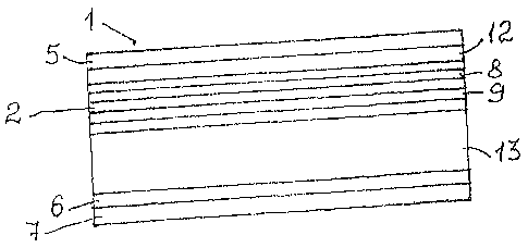
The proposed heterostructure 1 (see Fig. 1) contains one active layer 2, on
each side of which two leak-in regions 3 and 4 were adjacent. To the leak-in
regions
3 and 4 on each external (relative to the active layer 2) side two reflective
layers 5
and 6 were adjacent. The reflective layer 6 is located on the side of the
substrate 7 of
the n-type GaAs. The leak-in regions 3 and 4 each contains one main adjusting
layer
8 and 9 adjacent to the active layer 2 on each of its side, each one of
confining layers
10 and 11 adjacent respectively to the main adjusting layers 8 and 9, and each
one
of leak-in layers 12 and 13 adjacent respectively to the adjusting layers 10
and 11.
The active layer 2 is made of InGaAs with a thickness of 0.008 m. The laser
wavelength in such a heterostructure is equal to 980 nm. The main adjusting
layers 8
and 9 had the same thicknesses of 0.04 m and were grown of GaAs. The
confining
layers 10 and 11 had the same compositions of AI0.38Gao.62As and the same
thicknesses of 0.04 pm. The leak-in layers 12 and 13 had the same thicknesses
of
CA 02588076 2007-05-16
27
4.0 m and were grown of AI0.19Gao.$1As. Both reflective layers 5 and 6
consisted of
two sublayers of the same compositions and thicknesses. The first sublayers
14, 15
with a thickness of 0.5 m adjacent to corresponding leak-in layers were grown
of
AI0.2oGao_$oAs, the composition close to the composition of the leak-in layer;
the
second sublayers 16, 17 with a thickness of 0.6 m were grown of
A10.25Gao.75As. Let
us note that hereinafter to each composition of semiconductor layers for a
fixed
emission wavelength there is a certain corresponding refractive index. When
growing the HS 1, the active layer 2 and the main adjusting layers 8 and 9
were not
doped, the confining layers 10 (of the p-type) and 11 (of the n-type) were
doped with
the known impurities to 6=10" cm-3 and 3=10" cm-3 respectively, the leak-in
layers
12, 13 and the first sublayers 14, 16 of the reflective layers 5 and 6 of the
p-type and
the n-type respectively were doped to 1.1017 cm-3, and the second sublayers
15, 17
of the reflective layers 5 and 6 of the p-type and the n-type respectively
were doped
to 2-1018 cm-3.
The chosen compositions and thicknesses of the HS 1 layers provided at
current densities of 0.3 kA/cm2 and 10 kA/cm2 calculated values of the ratios
neff to
n,N of 1.000006 and 0.99964 respectively. The resulting amplification in the
active
layer at a current density of 0.35 kA/cm2 was 7.8 cm-'. The calculated angle
of
divergence 01 in the vertical plane at a current density of 10 kA/cm2 was 6.0
(hereinafter FWHM).
The following embodiment of the HS 1 differed from the above one that in this
embodiment the thicknesses of the leak-in layers 12 and 13 were identical and
equal
to 2.5 m. In this case the calculated values of the ratios neff to n,N at
current densities
of 0.3 kA/cm2 and 10 kA/cm2 were respectively 0.99992 and 0.99933. The
resulting
amplification at a current density of 0.3 kA/cm2 was 10.0 cm"'. The calculated
angle
of divergence 61 in the vertical plane at a current density of 10 kA/cm2 was
9.0 .
The following embodiment of the HS 1 (see Fig. 2) differed from the
embodiment schematically presented in Fig. 1 in that in this embodiment the
leak-in
layers 12 and 13 were grown of Al0_05Ga0.95As, and into the leak-in region,
together
with the main adjusting layers 8 and 9, two auxiliary adjusting layers 18 and
19 were
introduced additionally that were made of GaAs and located on each side of the
active layer between the confining layers 10 and 11 and the leak-in layers 12
and 13.
CA 02588076 2007-05-16
28
The obtained HS due to the low content of Al in the layers 12, 13 and 5, 6 had
reduced ohmic and thermal resistances and compressive mechanical stresses.
The following embodiment of the HS 1 (see Fig. 3) differed from the
embodiment schematically presented in Fig. 1 in that in this embodiment the
thicknesses of the leak-in layers 12 and 13 were respectively 0.5 m and 7.0
m,
and the thickness of the main adjusting layer 8 was 0.06 m. For this
embodiment of
the HS1 the calculated magnitudes of the ratios neff to nIN at current
densities of 0.3
kA/cm2 and 10 kA/cm2 were respectively 1.00004 and 0.99984. The resulting
amplification at a current density of 0.3 kA/cm2 was 10.2 cm-'. The calculated
angle
of divergence 6-L in the vertical plane at a current density of 10 kA/cm2 was
8.1 .
The following embodiment of the HS 1 (see Fig. 4) differed from the above in
that in this embodiment two identical active layers 2 were formed, the main
central
adjusting layer 20 of GaAs with a thickness of 0.012 m located between the
active
layers was introduced, and the thickness of the main adjusting layer 8 was
0.03 m.
For this embodiment of the HS I the calculated values of the ratios neff to
n,N at
current densities of 0.3 kA/cm2 and 10 kA/cm2 were respectively 1.00002 and
0.99984. The resulting amplification at a current density of 0.3 kA/cm2 was
8.9 cm-'.
The calculated angle of divergence @-L in the vertical plane at a current
density of 10
kA/cm2 was 8.1 .
The following embodiment of the HS 1 differed from the embodiment
schematically presented in Fig. 4 in that in this embodiment the main central
adjusting layer 20 consisted of two thin (each with a thickness of 0.005 m)
sublayers of the n-type and the p-type, doped respectively with tellurium and
carbon
to concentrations of 5.1019 cm-3. The sublayer of the n-type was placed on the
side of
the reflective layer of the p-type, and the sublayer of the p-type was placed
on the
side of the reflective layer of the n-type and the substrate of the n-type.
The following embodiment of the HS 1 differed from the embodiment
schematically presented in Fig. 1 in that in this embodiment the leak-in
layers 12 and
13 were made with the same composition (and therefore with the same refractive
index) as the confining layers 9 and 10, namely, of Al0,38Gao.62As, and the
reflective
layers 5 and 6 (without sublayers) had the composition AIo.45Gao.s5As. This
embodiment of the HS, as compared with the previous ones, contained a lesser
CA 02588076 2007-05-16
29
number of layers, however, it was characterized by increased values of ohmic
resistances, thermal resistances and compressive mechanical stresses.
The proposed Laser 30 (see Fig. 5) was made with the use of the
embodiment of the symmetric HS 1 presented in Fig. 1. To the substrate 7 of
the n-
type and the contact layer of the p-type formed on the opposite side (not
shown in
the Figures) the metallization layers (not shown in the Figures) were applied.
The
length of the optical resonator Lres was chosen equal to 2000 m. To the
cleaved
facets 31 the reflective coatings 32 and 33 with reflection coefficients
respectively R,
= 99% and R2 = 5% were applied. The stripe regions of current flow had a mesa
stripe width of 10 m. The calculated threshold current density jtnr was 350
A/cm2,
and the differential efficiency nd was about 88%. At all values of
overthreshold
current, up to 20 kA/cm2, the resulting amplification in the active layer was
more than
at j,hr. The angle of leak cp in this case varied from 0 to 1.65 , which
provided the
single-mode (in the vertical plane) operation of the Laser 30 in the range
from 0.35
kA/cm2 to 20 kA/cm2. The known calculated confinement factor 1' defining a
share of
laser emission propagating in the active layer 2 at a current density of 10
kA/cm2 was
3=10-4. The calculated angle of divergence 01 in the vertical plane decreased
from
7.8 (at a current density of 0.35 kA/cm2) to 6.0 (at 10 kA/cm2). The size of
the
emitting area at a level of 0.13 on the output optical facet of the resonator
in the
vertical plane varied from 5.7 m (at 0.35 kA/cm2) to 8.0 m (at 10 kA/cm2).
The proposed Laser 30 (see Fig. 6) was made with the use of the
embodiment of the symmetric HS I presented in Fig. 2, in which the leak-in
layers 12
and 13 as well as the first sublayers 14 and 16 of the refiective layers 5, 6
were
made with the a low content of Al of A(o0o5GaQ.85As and of Alo.osGao.8sAs
respectively.
In this case the auxiliary adjusting layers 18 and 19 were made of GaAs with
equal
thicknesses of 0.24 m. This embodiment of the Laser 30 had increased
efficiency,
power and reliability of operation.
The proposed Laser 30 (see Fig. 7) was made with the use of the
embodiment of the asymmetric HS 1 presented in Fig. 3, in which the leak-in
layers
12 and 13, identical in composition, had thicknesses respectively of 0.5 and
7.0 m.
By choosing thicknesses of the main adjusting layers 8 and 9 a threshold
current
density of 0.3 kA/cm2 was achieved. The calculated angle of divergence 81 in
the
CA 02588076 2007-05-16
vertical plane at first decreased from 7.50 (at a current density of 0.3
kA/cm2) to 7.2
(at 3 kA/cm2) and then increased to 8.1 (at 10 kA/cm2). In this case the size
of the
emitting area (at a level of 0.13) on the output optical facet of the
resonator in the
vertical plane at first increased from 4.6 m to 7.2 m and then decreased to
6.0 m.
5 The following embodiment of the Laser 30 differed from the above in that in
this embodiment the leak-in layers 12 and 13 were made with the same
composition
as the confining layers 9 and 10, namely, of Al0.38Gao.62As. The reflective
layers 5, 6
(without sublayers) were made of AIo.a5Gao.55As. This embodiment of the Laser
30,
as compared with the previous ones, contained a lesser number of layers of HS.
10 The proposed Laser 30 (see Fig. 8) was made with the use of the
embodiment of the asymmetric HS 1 presented in Fig. 4, in which two identical
active
layers 2 were made, and between them the main central adjusting layer 20 with
a
thickness of 0.012 m was placed. In this embodiment of the Laser 30 the
threshold
current density was reduced to 0.25 kA/cm2.
15 The following embodiment of the Laser 30 differed from the above in that
the
main central adjusting layer 20 consisted of two sublayers of the p-type and
the n-
type, each with a thickness of 0.005 m, doped respectively with carbon and
silicon
with equal concentrations of current carriers of 5.1019 cm-3. In operation of
the Laser
30 such sublayers provided the tunnel passage of current from one active layer
to
20 another, and at the same current, but approximately at the doubied applied
voltage,
output power increased by the power of two.
The proposed SAE 40 used also in the SOA was made on the basis of the
embodiment of the HS 1 presented in Fig. 1. The SAE 40 of this embodiment and
the
method of its manufacturing completely coincided with the embodiment of the
Laser
25 30 presented in Fig. 5, except that to the cleaved facets of the HS 1 the
clarifying
films with equal reflection coefficients R, and R2 of 0.01 % were applied. At
all values
of current the resulting ampiification in the active layer defined by the
compositions
and thicknesses of the heterostructure layers as well as by the refiection
coefficients
R, and R2 was less than its threshold value of self-excitation up to current
densities
30 of 10 kA/cm2 and more. The condition of emission leak from the active layer
to the
leak-in layers (with a signal at the input) began to be met in case of
exceeding a
current density more than 0.3 kA/cm2. The angle of leak cp in this case
increases from
CA 02588076 2007-05-16
31
0 at 0.3 kA/cm2 to 1.53 at 10 kA/cm2. The entrance aperture of the SAE 40 at
10
kA/cm2 was 8x10 m2, and the angular aperture was approximately 6.0 x 5.7 .
The following embodiment of the SAE 40 (see Fig. 9) used in the SOA differed
from the above by the width of the stripe region of current flow equal to 8
m, the
compositions and thicknesses of the HS 1 layers designed for a emission
wavelength
of 1305 nm, as well as in that to the optical facets 31 with the clarifying
films 41 and
42 (for which R, and R2 were identical and equal to 0.01%) the optical fibers
were
coupled: the input optical fiber 43 for input of emission through the input
optical facet
31 with the clarifying film 41 and the output optical fiber 44 for output of
emission
from the opposite optical facet 31 with the clarifying film 42. The sizes of
the entrance
and exit apertures of the SAE 40 equal to 10x10 m2 were in conformity with
the
apertures of the known optical fibers, which made it possible to couple the
input
optical fiber 43 and the output optical fiber 44 to the optical facets 31 with
the
corresponding coatings 41 and 42 directly, in immediate contact with the SAE
40.
This embodiment of the SAE 40 can be used with high efficiency as power
amplifiers,
optical switches, optical wavelength converters in modern fiber communication
links.
Its main advantage is reduced noise determined by low losses of input emission
in its
input into the SAE 40. The noise factor in this case can be comparable with
that of
fiber and Raman amplifiers. The near-square form of the region of propagation
of
amplified emission of 100 m2 makes the SAE 40 practically insensitive to
polarization of an input signal. A small-signal amplification of a signal in
such a SAE
40 more than 35 dB can be obtained, and the amplified power of emission
without its
saturation can reach 1 W and more. An advantage of the SAE 40 is also that its
output amplified emission is practically symmetric and has a low angular
divergence
of emission.
The following embodiment of the SAE 40 used in the SOA differed from the
above in that the introduced mesa stripe region of current flow was made
inclined to
the cavity of the optical facet at an angle of 7 . This has made it possible
to reduce
the requirements to the value of reflection coefficients R, and R2
approximately by an
order of magnitude (10 times).
The proposed SAE 40 used also in the SOA was made on the basis of the
embodiment of the HS 1 presented in Fig. 2. The SAE 40 of this embodiment and
the
CA 02588076 2007-05-16
32
method of its manufacturing completely coincided with the embodiment of the
Laser
30 presented in Fig. 6, except that to the cleaved facets of the HS 1 the
clarifying
films with equal reflection coefficients R, and R2 of 0.01 % were applied.
The proposed SAE 40 used also in the SOA was made on the basis of the
embodiment of the HS 1 presented in Fig. 3 and completely coincided with the
embodiment of the Laser 30 presented in Fig. 7, except that to the cleaved
facets of
the HS 1 the clarifying films with equal reflection coefficients R, and R2 of
0.01%
were applied.
The proposed SAE 40 used also in the SOA was made on the basis of the
embodiment of the HS I presented in Fig. 4 and completely coincided with the
embodiment of the Laser 30 presented in Fig. 8, except that to the cleaved
facets of
the HS 1 the clarifying films 41, 42 with equal reflection coefficients of
0.01% were
applied.
The following embodiment of the SAE 40 used also in the SOA differed from
the embodiment of the Laser 30 with two active layers with the tunnel passage
of
current between them only by reflection coefficients of the clarifying films
41, 42 of
0.01%.
The proposed SOA (see Fig. 10) comprises a master source of input emission
made as the Laser 30 optically coupled with the SAE 40. The Laser 30 and the
SAE
40 are made with the use of the same embodiment of the HS 1 described above
and
schematically presented in Fig. 1. The Laser 30 coincides with the above
embodiment schematically presented in Fig. 5. The distinction of the SAE 40
from
the Laser 30 consists in the clarifying films 41, 42 with equal reflection
coefficients of
0.01% applied to the cleaved facets 31. The stripe regions of current flow of
the
Laser 30 and the SAE 40 are made with the same width of 8 m. The exit
aperture of
the Laser 30 and the entrance aperture of the SAE 40 are identical and equal
to 8.0 x
8.0 m2, and the caiculated angles of divergence 81 in the vertical plane at a
current
density of 10 kA/cm2 are 6.0 . The output power of the Laser 30 in the single-
spatial-
mode operation for two transverse indices is 0.5 W. The large and equal output
aperture of the master Laser 30 and entrance aperture of the SAE 40 make it
possible to align the master Laser 30 and the SAE 40 on one longitudinal
optical axis
with a shortest distance between them with sufficient accuracy and low losses
of
CA 02588076 2007-05-16
33
emission. Such a SOA is a superhigh-power source of high-quality single-mode
and
single-frequency laser emission.
Industrial applicability
The heterostructures are used for creation of semiconductor injection
emission sources such as injection lasers,
CA 02588076 2007-05-16
34
semiconductor amplifying elements, semiconductor optical amplifiers that are
used in
fiber optic communication and data transmission systems, in optical superhigh-
speed
computing and switching systems, in development of medical equipment, laser
industrial equipment, frequency-doubled lasers, and for pumping solid-state
and fiber
amplifiers and lasers.