Note: Descriptions are shown in the official language in which they were submitted.
CA 02588357 2007-05-08
MOBILE WIRELESS COMMUNICATIONS DEVICE
HAVING LOW-IF RECEIVER CIRCUITRY THAT ADAPTS TO
RADIO ENVIRONMENT
Field of the Invention
The present invention relates to the field of communications devices, and more
particularly, to mobile wireless communications devices and related systems
and methods
that use low IF receiver circuitry that adapts to the radio environment.
Back2round of the Invention
Cellular communication systems continue to grow in popularity and have become
an integral part of both personal and business communications. Cellular
telephones and
similar devices allow users to place and receive phone calls most anywhere
they travel.
Moreover, as cellular telephone technology is increased, so too has the
functionality of
cellular devices. For example, many cellular devices now incorporate Personal
Digital
Assistant (PDA) features such as calendars, address books, task lists,
calculators, memo
and writing programs, etc. These multi-function devices usually allow users to
send and
receive electronic mail (email) messages wirelessly and access the internet
via a cellular
network and/or a wireless local area network (WLAN), for example.
Many of the cellular communications use packet burst transmissions as part of
a
Global System for Mobile communications (GSM) system, which includes the 450
MHz,
900 MHz, 1800 MHz and 1900 MHz frequency bands. The current generation of
wireless
transceivers typically use two main types of receiver architectures, i.e., a
direct conversion
receiver architecture or a digital low-IF receiver architecture (also termed
very low-IF, i.e.,
VLIF), thus, eliminating much of the prior generation analog down conversion
stage.
Much of the expensive and bulky intermediate frequency (IF) components used in
conventional superheterodyne receivers has been eliminated with direct
conversion and
low-IF receiver architecture. In a direct conversion receiver, a signal is
converted directly
to baseband, while in a digital low-IF receiver, some advantages of the
superheterodyne
remain with the economic and integrated advantages of a direct conversion
receiver.
In a low-IF receiver, on the other hand, the RF signal can be mixed down to a
non-
zero low or moderate intermediate frequency, typically a few megahertz in some
1
CA 02588357 2007-05-08
examples. Thus, the low-IF receiver architecture includes many of the
desirable properties
of the zero-IF receiver architectures, yet still avoids DC offset and some 1/F-
noise
problems. The non-zero IF receiver architecture will reintroduce some signal
image
issues. In a low-IF receiver, the RF signal is band selected and downconverted
to the
frequency close to baseband, sometimes as close as 100 KHz. This low-IF signal
can be
filtered with a low pass filter and amplifier before its conversion to the
digital domain by
an analog-to-digital converter (ADC). Any final signal downconversion for
baseband and
fine gain control can be performed digitally in a processor.
It is also possible to incorporate some high-resolution, oversampling and
delta-
sigma converters to permit channel filtering, including the use of digital
signal processing
(DSP) techniques rather than analog filters. The signal could interface to a
digital
processor or a digital-to-analog converter and output analog Inphase (I) and
Quadrature
(Q) signals to the processor.
An important GSM receiver parameter is the rejection of interferer signals to
enhance performance of the low-IF receiver. European Telecommunications
Standards
Institute (ESTI) mobile station conformance specifies very strict
certification tests (14.5,
14.18.3) that are not easy to pass using GSM receivers currently available on
the market.
Even if a receiver passes certification tests, having better performance
resulting from
interferer signal rejection may significantly improve end-user experience in
large urban
areas, where strong radio interference is a common problem.
Rejection of interferer signals is usually a problem for very low-IF receiver
architecture where rejection performance is limited by UQ gain and phase
imbalance. The
common way to address this problem is to use I/Q imbalance calibration where
UQ gain
and phase will be adjusted during digital baseband processing based on
previously
calculated calibration tables. Unfortunately, these types of calibration
processes do not
provide enough accuracy when time measurements during calibration cycle are
limited. If
the calibration time is extended, however, the manufacturing costs for a
single
communications device may increase significantly.
Some proposals to solve such problems toggle the local oscillator (LO) with a
"round-robin" scheme using a low-side LO injection during one receive (RX)
session and
a high-side LO injection in another session. This solution does not use any
feedback from
the radio environment, thus achieving only a basic "averaging" of the
interferer image.
2
CA 02588357 2007-05-08
There is typically no knowledge of the external environment. Also, by not
taking the type
of signal used in the receive session into account, results in a worst case
scenario when,
for example, distorted signal bursts are mixed with Received Signal Strength
Indication
(RSSI) measurements, and the resulting data stream picks the worst interferer
appearance.
Summary of the Invention
In accordance with non-limiting examples, a mobile wireless communications
device includes a housing and circuit board carried by the housing. The
circuit board
includes a radio frequency (RF) circuit and processor operative with each
other. The RF
circuitry includes a low-IF receiver circuit that is operative for maintaining
an interferer
signal at the same frequency as a wanted signal relative to a local oscillator
frequency
setting, creating an interferer image signal, and filtering the image signal
at substantially
baseband frequency.
A radio frequency (RF) circuit can include a Digital Signal Processing (DSP)
circuit that is operative for filtering the interferer image signal. The RF
circuitry can be
operative for placing an interferer signal in the substantially baseband
frequency where a
highest out-of-band signal attenuation is implemented.
In yet another aspect, the RF circuitry can include at least one mixer circuit
and a
local oscillator circuit. A demodulator circuit that could comprise an analog-
to-digital
converter, digital mixer and processor is operative for demodulating signals.
The RF
circuitry is operative for determining between the better performing local
oscillator
frequency setting and a poorer performing local oscillator frequency setting
based on
signal-to-noise values obtained during demodulation. The RF circuitry can also
be
operative for using different low-IF local oscillator frequency settings for
an RF channel
based on the signal-to-noise values.
The communications signals can be formed as data bursts in accordance with the
global system for mobile communications. The RF circuitry can also be
operative for
returning to a poorer performing local oscillator frequency setting from a
better
perfonning local oscillator frequency setting after a predetermined number of
received
data bursts to determine if the local oscillator frequency setting should be
changed to adapt
to a changed radio environment.
A method aspect and radio receiver are also set forth.
3
CA 02588357 2007-05-08
Brief Description of the Drawin2s
Other objects, features and advantages will become apparent from the detailed
description which follows when considered in light of the accompanying
drawings in
which:
FIG. 1 is a schematic block diagram of an example of a mobile wireless
communications device configured as a handheld device that can be used in
accordance
with non-limiting examples and illustrating basic internal components thereof.
FIG. 2 is a front elevation view of the mobile wireless communications device
of
FIG. 1.
FIG. 3 is a schematic block diagram showing basic functional circuit
components
that can be used in the mobile wireless communications device of FIGS. 1-2.
FIG. 4 is a high-level, schematic circuit and block diagram of a low-IF
receiver
that can use the system and method for adapting to the environment in
accordance with
non-limiting examples.
FIG. 5 is a graph showing an interferer signal, a wanted signal and a local
oscillator (signal) having a negative frequency offset from the desired
central frequency.
FIG. 6 is a graph similar to that shown in FIG. 5, but after radio frequency
(RF)
downconversion, and showing the interferer image signal that appears and
results from the
I/Q imbalance for the amplitude and phase.
FIG. 7 is a graph similar to FIG. 5, and showing the interferer signal and
wanted
signals and a positive side local oscillator signal and having a positive
frequency offset.
FIG. 8 is a graph similar to FIG. 7, and showing the interferer signal and the
wanted signal and the wanted signal image and interferer image.
Detailed Description of the Preferred Embodiments
Different embodiments will now be described more fully hereinafter with
reference
to the accompanying drawings, in which preferred embodiments are shown. Many
different forms can be set forth and described embodiments should not be
construed as
limited to the embodiments set forth herein. Rather, these embodiments are
provided so
that this disclosure will be thorough and complete, and will fully convey the
scope to those
skilled in the art. Like numbers refer to like elements throughout.
4
CA 02588357 2007-05-08
In accordance with one non-limiting example, the limitations caused by, for
example, calibration time being extended can be overcome by adjusting the
radio
frequency (RF) circuit configuration at "run time" based on the current radio
environment
"quality." Thus, an issue that is addressed is the strong, narrow-band
(unmodulated)
interferer rejection, which is addressed by placing the interferer in the
baseband frequency
where the highest out-of-band signal attenuation is implemented. Since most of
the very
low-IF receivers have non-symmetrical frequency response, this could aid in
preventing
signal waveform clipping in baseband analog/digital converters.
The system and method can be based on radio channel feedback statistics, for
example, the statistics of the signal-to-noise (SNR) ratio from the
demodulation of the
GSM bursts that are collected during regular receiver operation. SNR
statistics can be
collected for all used GSM channels. Different low-IF local oscillator (LO)
frequencies or
frequency settings can be used for the same channel. As soon as a strong
interferer
appears either in the lower or the higher frequency, the SNR from the GSM
burst
demodulation will identify which LO frequency setting has a worst or poorer
performing
performance compared to other LO settings. The proposed algorithtn creates a
map of all
used radio channels and will try to adjust the local oscillator frequency
setting "on-the-fly"
to receive the signals using the "best guess," i.e., better performing LO
configuration. The
system and method can use an algorithm that could return to the worst or
poorer
performing case LO frequency configuration after a predefined amount of
received
sessions to check for any radio environment "improvements." As a result, the
system and
method can maintain the interferer at the same frequency side as the wanted
signal relative
to the LO frequency setting, thus creating an interferer "image" out of the
wanted signal
band, and filtered out in the baseband Digital Signal Processing (DSP)
circuit.
A brief description will now proceed relative to FIGS. 1-3, which disclose an
example of a mobile wireless communications device, for example, a handheld
portable
cellular radio, which can incorporate non-limiting examples of various
circuits that can be
used with the low-IF receiver circuitry that adapts to the environment as will
be described
below. FIGS. 1-3 are representative non-limiting examples of the many
different types of
functional circuit components and their interconnection, and operative for use
with low-IF
receiver circuitry.
CA 02588357 2007-05-08
Referring initially to FIGS. 1 and 2, an example of a mobile wireless
communications device 20, such as a handheld portable cellular radio is first
described.
This device 20 illustratively includes a housing 21 having an upper portion 46
and a lower
portion 47, and a dielectric substrate (i.e., circuit board) 67, such as a
conventional printed
circuit board (PCB) substrate, for example, carried by the housing. A housing
cover (not
shown in detail) would typically cover the front portion of the housing. The
term circuit
board 67 as used hereinafter can refer to any dielectric substrate, PCB,
ceramic substrate
or other circuit carrying structure for carrying signal circuits and
electronic components
within the mobile wireless communications device 20. The illustrated housing
21 is a
static housing, for example, as opposed to a flip or sliding housing which are
used in many
cellular telephones. However, these and other housing configurations may also
be used.
Circuitry 48 is carried by the circuit board 67, such as a microprocessor,
memory,
one or more wireless transceivers (e.g., cellular, WLAN, etc.), which includes
RF
circuitry, including audio and power circuitry, including any keyboard
circuitry. It should
be understood that keyboard circuitry could be on a separate keyboard, etc.,
as will be
appreciated by those skilled in the art. A battery (not shown) is also
preferably carried by
the housing 21 for supplying power to the circuitry 48. The term RF circuitry
could
encompass the interoperable RF transceiver circuitry, power circuitry and
audio circuitry.
Furthermore, an audio output transducer 49 (e.g., a speaker) is carried by an
upper
portion 46 of the housing 21 and connected to the circuitry 48. One or more
user input
interface devices, such as a keypad (keyboard) 23 (FIG. 2), is also preferably
carried by
the housing 21 and connected to the circuitry 48. The term keypad as used
herein also
refers to the term keyboard, indicating the user input devices having lettered
and/or
numbered keys commonly known and other embodiments, including multi-top or
predictive entry modes. Other examples of user input interface devices include
a scroll
wheel 37 and a back button 36. Of course, it will be appreciated that other
user input
interface devices (e.g., a stylus or touch screen interface) may be used in
other
embodiments.
An antenna 45 is preferably positioned at the lower portion 47 in the housing
and
can be fonned as a pattern of conductive traces that make an antenna circuit,
which
physically forms the antenna. It is connected to the circuitry 48 on the main
circuit board
67. In one non-limiting example, the antenna could be formed on an antenna
circuit board
6
CA 02588357 2007-05-08
section that extends from the main circuit board at the lower portion of the
housing. By
placing the antenna 45 adjacent the lower portion 47 of the housing 21, the
distance is
advantageously increased between the antenna and the user's head when the
phone is in
use to aid in complying with applicable SAR requirements. Also, a separate
keyboard
circuit board could be used.
More particularly, a user will typically hold the upper portion of the housing
21
very close to his head so that the audio output transducer 49 is directly next
to his ear.
Yet, the lower portion 47 of the housing 21 where an audio input transducer
(i.e.,
microphone) is located need not be placed directly next to a user's mouth, and
can be held
away from the user's mouth. That is, holding the audio input transducer close
to the user's
mouth may not only be uncomfortable for the user, but it may also distort the
user's voice
in some circumstances. In addition, the placement of the antenna 45 adjacent
the lower
portion 47 of the housing 21 also advantageously spaces the antenna farther
away from the
user's brain.
Another important benefit of placing the antenna 45 adjacent the lower portion
47
of the housing 21 is that this may allow for less impact on antenna
performance due to
blockage by a user's hand. That is, users typically hold cellular phones
toward the middle
to upper portion of the phone housing, and are therefore more likely to put
their hands
over such an antenna than they are an antenna mounted adjacent the lower
portion 47 of
the housing 21. Accordingly, more reliable performance may be achieved from
placing
the antenna 45 adjacent the lower portion 47 of the housing 21.
Still another benefit of this configuration is that it provides more room for
one or
more auxiliary input/output (UO) devices 50 to be carried at the upper portion
46 of the
housing. Furthermore, by separating the antenna 45 from the auxiliary I/O
device(s) 50,
this may allow for reduced interference therebetween.
Some examples of auxiliary UO devices 50 include a WLAN (e.g., Bluetooth,
IEEE 802.11) antenna for providing WLAN communication capabilities, and/or a
satellite
positioning system (e.g., GPS, Galileo, etc.) antenna for providing position
location
capabilities, as will be appreciated by those skilled in the art. Other
examples of auxiliary
I/O devices 50 include a second audio output transducer (e.g., a speaker for
speaker phone
operation), and a camera lens for providing digital camera capabilities, an
electrical device
connector (e.g., USB, headphone, secure digital (SD) or memory card, etc.).
7
CA 02588357 2007-05-08
It should be noted that the term "input/output" as used herein for the
auxiliary UO
device(s) 50 means that such devices may have input and/or output
capabilities, and they
need not provide both in all embodiments. That is, devices such as camera
lenses may
only receive an optical input, for example, while a headphone jack may only
provide an
audio output.
The device 20 further illustratively includes a display 22, for example, a
liquid
crystal display (LCD) carried by the housing 21 and connected to the circuitry
48. A back
button 36 and scroll wheel 37 can also be connected to the circuitry 48 for
allowing a user
to navigate menus, text, etc., as will be appreciated by those skilled in the
art. The scroll
wheel 37 may also be referred to as a "thumb wheel" or a "track wheel" in some
instances.
The keypad 23 illustratively includes a plurality of multi-symbol keys 24 each
having
indicia of a plurality of respective symbols thereon. The keypad 23 also
illustratively
includes an alternate function key 25, a next key 26, a space key 27, a shift
key 28, a
return (or enter) key 29, and a backspace/delete key 30.
The next key 26 is also used to enter a"*" symbol upon first pressing or
actuating
the alternate function key 25. Similarly, the space key 27, shift key 28 and
backspace key
30 are used to enter a "0" and "#", respectively, upon first actuating the
alternate function
key 25. The keypad 23 further illustratively includes a send key 31, an end
key 32, and a
convenience (i.e., menu) key 39 for use in placing cellular telephone calls,
as will be
appreciated by those skilled in the art.
Moreover, the symbols on each key 24 are arranged in top and bottom rows. The
symbols in the bottom rows are entered when a user presses a key 24 without
first pressing
the alternate function key 25, while the top row symbols are entered by first
pressing the
alternate function key. As seen in FIG. 2, the multi-symbol keys 24 are
arranged in the
first three rows on the keypad 23 below the send and end keys 31, 32.
Furthermore, the
letter symbols on each of the keys 24 are arranged to define a QWERTY layout.
That is,
the letters on the keypad 23 are presented in a three-row format, with the
letters of each
row being in the same order and relative position as in a standard QWERTY
keypad.
Each row of keys (including the fourth row of function keys 25-29) is arranged
in
five columns. The multi-symbol keys 24 in the second, third, and fourth
columns of the
first, second, and third rows have numeric indicia thereon (i.e., 1 through 9)
accessible by
first actuating the alternate function key 25. Coupled with the next, space,
and shift keys
8
CA 02588357 2007-05-08
26, 27, 28, which respectively enter a"*", "0", and "#" upon first actuating
the alternate
function key 25, as noted above, this set of keys defines a standard telephone
keypad
layout, as would be found on a traditional touch-tone telephone, as will be
appreciated by
those skilled in the art.
Accordingly, the mobile wireless communications device 20 as described may
advantageously be used not only as a traditional cellular phone, but it may
also be
conveniently used for sending and/or receiving data over a cellular or other
network, such
as Internet and email data, for example. Of course, other keypad
configurations may also
be used in other embodiments. Multi-tap or predictive entry modes may be used
for
typing e-mails, etc. as will be appreciated by those skilled in the art.
The antenna 45 is preferably formed as a multi-frequency band antenna, which
provides enhanced transmission and reception characteristics over multiple
operating
frequencies. More particularly, the antenna 45 is designed to provide high
gain, desired
impedance matching, and meet applicable SAR requirements over a relatively
wide
bandwidth and multiple cellular frequency bands. By way of example, the
antenna 45
preferably operates over five bands, namely a 850 MHz Global System for Mobile
Communications (GSM) band, a 900 MHz GSM band, a DCS band, a PCS band, and a
WCDMA band (i.e., up to about 2100 MHz), although it may be used for other
bands/frequencies as well. To conserve space, the antenna 45 may
advantageously be
implemented in three dimensions although it may be implemented in two-
dimensional or
planar embodiments as well.
The mobile wireless communications device shown in FIGS. I and 2 can
incorporate e-mail and messaging accounts and provide different functions such
as
composing e-mail, PIN messages, and SMS messages. The device can manage
messages
through an appropriate menu that can be retrieved by choosing a messages icon.
An
address book function could add contacts, allow management of an address book,
set
address book options and manage SIM card phone books. A phone menu could allow
for
the making and answering of phone calls using different phone features,
managing phone
call logs, setting phone options, and viewing phone information. A browser
application
could permit the browsing of web pages, configuring a browser, adding
bookmarks, and
changing browser options. Other applications could include a task, memo pad,
calculator,
alarm and games, as well as handheld options with various references.
9
CA 02588357 2007-05-08
A calendar icon can be chosen for entering a calendar program that can be used
for
establishing and managing events such as meetings or appointments. The
calendar
program could be any type of messaging or appointment/meeting program that
allows an
organizer to establish an event, for example, an appointment or meeting.
A non-limiting example of various functional components that can be used in
the
exemplary mobile wireless communications device 20 of FIGS. 1 and 2 is further
described in the example below with reference to FIG. 3. The device 20
illustratively
includes a housing 120, a keypad 140 and an output device 160. The output
device 160
shown is preferably a display, which is preferably a full graphic LCD. Other
types of
output devices may alternatively be used. A processing device 180 is contained
within the
housing 120 and is coupled between the keypad 140 and the display 160. The
processing
device 180 controls the operation of the display 160, as well as the overall
operation of the
mobile device 20, in response to actuation of keys on the keypad 140 by the
user.
The housing 120 may be elongated vertically, or may take on other sizes and
shapes (including clamshell housing structures). The keypad may include a mode
selection
key, or other hardware or software for switching between text entry and
telephony entry.
In addition to the processing device 180, other parts of the mobile device 20
are
shown schematically in FIG. 3. These include a communications subsystem 101; a
short-
range communications subsystem 102; the keypad 140 and the display 160, along
with
other input/output devices 106, 108, 110 and 112; as well as memory devices
116, 118 and
various other device subsystems 121. The mobile device 20 is preferably a two-
way RF
communications device having voice and data communications capabilities. In
addition,
the mobile device 20 preferably has the capability to communicate with other
computer
systems via the Internet.
Operating system software executed by the processing device 180 is preferably
stored in a persistent store, such as the flash memory 116, but may be stored
in other types
of memory devices, such as a read only memory (ROM) or similar storage
element. In
addition, system software, specific device applications, or parts thereof, may
be
temporarily loaded into a volatile store, such as the random access memory
(RAM) 118.
Communications signals received by the mobile device may also be stored in the
RAM
118.
CA 02588357 2007-05-08
The processing device 180, in addition to its operating system functions,
enables
execution of software applications 130A-130N on the device 20. A predetermined
set of
applications that control basic device operations, such as data and voice
communications
130A and 130B, may be installed on the device 20 during manufacture. In
addition, a
personal information manager (PIM) application may be installed during
manufacture.
The PIM is preferably capable of organizing and managing data items, such as e-
mail,
calendar events, voice mails, appointments, and task items. The PIM
application is also
preferably capable of sending and receiving data items via a wireless network
141.
Preferably, the PIM data items are seamlessly integrated, synchronized and
updated via
the wireless network 141 with the device user's corresponding data items
stored or
associated with a host computer system.
Communication functions, including data and voice communications, are
performed through the communications subsystem 101, and possibly through the
short-
range communications subsystem. The communications subsystem 101 includes a
receiver
150, a transmitter 152, and one or more antennae 154 and 156. In addition, the
communications subsystem 101 also includes a processing module, such as a
digital signal
processor (DSP) 158, and local oscillators (LOs) 161. The specific design and
implementation of the communications subsystem 101 is dependent upon the
communications network in which the mobile device 20 is intended to operate.
For
example, the mobile device 20 may include a communications subsystem 101
designed to
operate with the MobitexTM, Data TACTM or General Packet Radio Service (GPRS)
mobile data communications networks, and also designed to operate with any of
a variety
of voice communications networks, such as AMPS, TDMA, CDMA, PCS, GSM, etc.
Other types of data and voice networks, both separate and integrated, may also
be utilized
with the mobile device 20.
Network access requirements vary depending upon the type of communication
system. For example, in the Mobitex and DataTAC networks, mobile devices are
registered on the network using a unique personal identification number or PIN
associated
with each device. In GPRS networks, however, network access is associated with
a
subscriber or user of a device. A GPRS device therefore requires a subscriber
identity
module, commonly referred to as a SIM card, in order to operate on a GPRS
network.
11
CA 02588357 2007-05-08
When required network registration or activation procedures have been
completed,
the mobile device 20 may send and receive communications signals over the
communication network 141. Signals received from the communications network
141 by
the antenna 154 are routed to the receiver 150, which provides for signal
amplification,
frequency down conversion, filtering, channel selection, etc., and may also
provide analog
to digital conversion. Analog-to-digital conversion of the received signal
allows the DSP
158 to perform more complex communications functions, such as demodulation and
decoding. In a similar manner, signals to be transmitted to the network 141
are processed
(e.g., modulated and encoded) by the DSP 158 and are then provided to the
transmitter
152 for digital to analog conversion, frequency up conversion, filtering,
amplification and
transmission to the communication network 141 (or networks) via the antenna
156.
In addition to processing communications signals, the DSP 158 provides for
control of the receiver 150 and the transmitter 152. For example, gains
applied to
communications signals in the receiver 150 and transmitter 152 may be
adaptively
controlled through automatic gain control algorithms implemented in the DSP
158.
In a data communications mode, a received signal, such as a text message or
web page
download, is processed by the communications subsystem 101 and is input to the
processing device 180. The received signal is then further processed by the
processing
device 180 for an output to the display 160, or alternatively to some other
auxiliary I/O
device 106. A device user may also compose data items, such as e-mail
messages, using
the keypad 140 and/or some other auxiliary I/O device 106, such as a touchpad,
a rocker
switch, a thumb-wheel, or some other type of input device. The composed data
items may
then be transmitted over the communications network 141 via the communications
subsystem 101.
In a voice communications mode, overall operation of the device is
substantially
similar to the data communications mode, except that received signals are
output to a
speaker 110, and signals for transmission are generated by a microphone 112.
Alternative
voice or audio IlO subsystems, such as a voice message recording subsystem,
may also be
implemented on the device 20. In addition, the display 160 may also be
utilized in voice
communications mode, for example to display the identity of a calling party,
the duration
of a voice call, or other voice call related information.
12
CA 02588357 2007-05-08
Any short-range communications subsystem enables communication between the
mobile device 20 and other proximate systems or devices, which need not
necessarily be
similar devices. For example, the short-range communications subsystem may
include an
infrared device and associated circuits and components, or a BluetoothTM
communications
module to provide for communication with similarly-enabled systems and
devices.
It should be understood that GSM is a preferred communications system and uses
a
radio interface that can have an uplink frequency band and downlink frequency
band with
about 25 MHz bandwidth, typically subdivided into 124 carrier frequency
channels, each
spaced about 200 KHz apart as non-limiting examples. Time division
multiplexing can be
used to allow about 8 speech channels per radio frequency channel, giving 8
radio time
slots and 8 burst periods grouped into what is called a TDMA frame. For
example, a
channel data rate could be about 270.833 Kbps and a frame duration of about
4.615
milliseconds (MS) in one non-limiting example. The power output can vary from
about I
to about 2 watts.
Typically, linear predictive coding (LPC) can be used to reduce the bit rate
and
provide parameters for a filter to mimic a vocal track with speech encoded at
about 13
Kbps. Four different cell sizes can be used in a GSM network, including macro,
micro,
pico and umbrella cells. A base station antenna can be installed on a master
building
above the average rooftop level in a macrocell. In a microcell, the antenna
height can be
under the average rooftop level and used in urban areas. Microcells typically
have a
diameter of about a few dozen meters and are used indoors. Umbrella cells can
cover
shadowed regions or smaller cells. Typically, the longest distance for the GSM
specification covered by an antenna is about 22 miles depending on antenna
height, gain
and propagation conditions.
GSM systems typically include a base station subsystem, a network and
switching
subsystem, and a General Packet Radio Service (GPRS) core network. A
subscriber
identify module (SIM) is usually implemented in the communications device, for
example,
the well known SIM card, similar to a smart card containing the subscription
information
and phone book of a user. The user can also switch handsets or could change
operators by
changing a SIM.
The GSM signaling protocol has three general layers. Layer 1 is a physical
layer
using channel structures above the air interface. Layer 2 is the data link
layer. Layer 3 is
13
CA 02588357 2007-05-08
a signaling protocol, which includes three sublayers. These include a Radio
Resources
Management sublayer to control the setup, maintenance and termination of radio
and fixed
channels, including handovers. A Mobility Management sublayer manages the
location
updating and registration procedures and secures the authentication. A
Connection
Management sublayer handles general call control and manages supplementary
services
and the short message service. Signaling between different entities such as
the Home
Location Register (HLR) and Visiting Location Register (VLR) can be
accomplished
through a Mobile Application Part (MAP) built upon the Transaction
Capabilities
Application Part (TCAP) of the top layer of the Signaling System No. 7.
A Radio Resources Management (RRM) sublayer can oversee the radio and fixed
link establishment between the mobile station and an MSE.
It is also possible to used Enhanced Data Rates for GSM Evolution (EDGE), as
an
enhancement to General Packet Radio Service (GPRS) networks. EDGE can use 8
Phase
Shift Keying (8 PSK) and Gaussian Minimum Shift Keying (GMSK) for different
modulation and coding schemes. A three-bit word can be produced for every
changing
carrier phase. A rate adaptation algorithm can adapt the Modulation and Coding
Scheme
(MCS) according to the quality of the radio channel and the bit rate and
robustness of data
transmission. Base stations are typically modified for EDGE use.
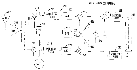
FIG. 4 is an example of a high-level block diagram and schematic circuit for a
low-
IF receiver that can be used with the system and method as described. The
receiver 200
includes an antenna 202 that receives a communications signal and passes the
signal to a
low noise amplifier (LNA) 204. The signal is split within a splitter 206 and
passes into
mixers 208, 210. A signal generator 212 generates a local oscillator (LO)
signal to the
mixers 208, 210. One of the local oscillator signals is phase changed by a non-
ideal
hybrid source or shifter 214, creating phase imbalance at broadband.
Respective signals
are passed from respective mixers 208, 210 as illustrated. Each signal passes
into
respective anti-alias filters 216, 218 and then into respective analog/digital
converters 220,
222. Digital mixing and demodulation occurs next. Each signal after conversion
passes
into a digital mixer circuit that includes multipliers 226, 228, with each
also receiving a
signal from a Direct Digital Synthesizer 224 as sine and cosine signals as
illustrated. The
signals from the Direct Digital Synthesizer 224 are multiplied in multipliers
230, 232 and
summed within summer 234 as part of digital mixing. Signals from mixers 226,
228 are
14
CA 02588357 2007-05-08
summed at summer 236. The signals from the summers 234, 236 are respectively
filtered
by selectivity filters 238, 240 and then processed within processor 242. The
anti-alias
filters can be non-ideal analog filters as a source of amplitude and phase
imbalance at
baseband.
In operation, after mixing in mixers 208, 210, the downconversion process
begins.
The mixer imbalance can create image problems as noted before. For example,
negative
frequencies can be translated to positive frequencies with significant
attenuation. The
Direct Digital Synthesizer with the multiplers can allow the shifting down to
zero.
FIGS. 5-8 are graphs showing two possible scenarios for the local oscillator
signal,
also referred to more conveniently as LO, where the local oscillator can
appear in the radio
frequency RF, as illustrated. FIGS. 5 and 6 show the negative side LO. FIG. 5
shows the
LO with a negative frequency offset from the central frequency of the wanted
signal (WS).
The interferer signal (IS) is shown on the left and the wanted signal on the
right. The
signal overlap shows the negative side LO. After the RF downconversion as
shown in
FIG. 6, the interferer image (II) appears because of the I/Q imbalance with
the amplitude
and phase.
FIGS. 7 and 8 are graphs showing preferred examples with scenarios of the
interferer and wanted signal, and the positive side LO with the positive
frequency offset.
FIG. 8 shows the interferer signal and wanted signal on the left side, and the
wanted image
(WI) and interferer image (II) on the right side as illustrated.
It should be understood that FIGS. 5 and 6 illustrate when the LO is between
the
two signals of the wanted and interferer, and thus, as the negative side LO
because it is
below the center of the wanted signal. After downconversion as shown in FIG.
6, the LO
appears to be zero DC at a basically zero Hz interferer on the negative side.
Because of
this UQ imbalance, the image of the interferer significantly reduces and the
overlap
appears with the wanted signal. The wanted signal appears to be degraded
significantly
because of the image that overlaps.
FIGS. 7 and 8 show the LO at the positive side such that after downconversion,
the
interferer on one side is relative to zero and there will be no overlap as the
wanted signal.
The selectivity filter as described before could remove some unwanted
components,
leaving wanted signals. Thus, it should be understood that in these examples,
FIGS. 5 and
6 represent a case with bad performance, and FIGS. 7 and 8 represent a case
with good
CA 02588357 2007-05-08
performance. The system attempts to reach the better position of the local
oscillator and
tries to maintain the interferer signal on the same side on the wanted signal.
There follows next a pseudocode description using C programming for the system
and method. It should be understood that the local oscillator in very low-IF
receivers
produces a single tone as an unmodulated carrier for the RF mixer input at a
wanted GSM
channel RF frequency, plus/minus very-low-IF, such that the system and method
can
dynamically choose the sign of the very-low-IF to obtain the best signal-to-
noise ratio
(SNR).
Three threads are described, each thread corresponding to a task of processing
in
the computer program. System initialization is a first thread that occurs one
time,
followed by a radio control thread and receiver demodulator thread, which are
repeated
continuously in a loop.
Pseudocode Description
System initialization:
1. Allocate array CURRENT_LO_COUNTER for all available GSM channels. Set
all entries to "0". This array defines how many times we will use currently
winning LO
side (with best SNR) until it will reach "0".
2. Allocate array LO_SIDE for all available GSM channels. Set all entries to
"0"
("0" means low side LO with negative Very_Low_IF; "1" means high side LO with
positive Very_Low_IF). This array will define currently used sign of
Very_Low_IF.
3. Allocate array TOP_LO_COUNTER for all available GSM channels. Set all
entries to "I". This array defines maximum numbers of tries system may apply
best LO
settings to particular channel without switching back to "worst" LO side to
look for
changes in the channel conditions.
4. Allocate array WINNING_LO_SNR for all available GSM channels. Set all
entries to "0". This array contains SNRs of the winning LO side for each GSM
channel.
Radio control thread:
1. If RF driver have to configure RF chipset to receive a regular GSM/GPRS
burst
then:
1.1. If CURRENT_LO_COUNTER for current GSM channel equal to "0" then
program RF chipset to use logical inversion of current LO_SIDE (inverse
Very_Low_IF
sign).
16
CA 02588357 2007-05-08
1.2. If CURRENT_LO_COUNTER for current GSM channel is larger then "0"
then program RF chipset to use current LO_SIDE (keep the same Very Low_IF
sign).
Receiver demodulator thread:
1. Demodulate received GSM/GPRS burst and get burst SNR.
2. If CURRENT_LO_COUNTER for current channel is equal to "0" (current SNR
represents loosing LO side) then:
2.1. Set CURRENT_LO_COUNTER equal to TOP_LO_COUNTER for the
current channel.
2.2. If current SNR is larger then WINNING_LO_SNR then:
2.2.1. If TOP_LO_COUNTER is equal to "1" (lowest possible
TOP_LO_COUNTER) then:
2.2.1.1. Inverse current LO_SIDE (we have new winning LO side).
2.2.1.2. Update current WINNING_LO_SNR with current SNR value.
2.2.1.3. Set CURRENT LO COUNTER to "0".
2.2.2. If TOP LO COUNTER is LARGER then "1" then decrement
TOP_LO_COUNTER.
2.3. If current SNR is smaller then WINNING LO SNR then increment
TOP_LO_COUNTER (but no higher then defined maximum limit, in my implementation
the highest possible TOP_LO_COUNTER = 60).
3. If CURRENT_LO_COUNTER for current channel is NOT equal to "0" then:
3.1. Store current SNR in the WINNING_LO_SNR array entry (corresponding to
current channel).
3.2. Decrement CURRENT LO COUNTER for the current channel.
In the pseudocode above, SNR indicates the signal-to-noise ratio. IF indicates
the
Intermediate Frequency. LO indicates the local oscillator. It should be
understood that in
very low intermediate frequency receivers, it produces a single tone typically
as an
unmodulated carrier for the RF mixer input at the wanted GSM channel RF
frequency as
+/- very-low-IF. The system and method dynamically chooses the sign of the
very-low-IF
to obtain the best SNR.
It should be understood that an array is a collection of variables of the same
type.
Individual array elements can be identified by an integer index. In C the
index typically
begins at zero. There can be single dimensioned arrays or multiple dimensional
arrays. It
17
CA 02588357 2007-05-08
should be understood that a pointer can be used in place of an array. Also,
typically
dimensions are not fixed immediately. Space can be allocated as required. When
passed
as an argument to a function, the size of the array is not necessarily known.
Although
traditionally some array types in C were one-dimensional, and a fixed, static
size specified
a compile time, there are variable length arrays that can be used. A block of
memory of
arbitrary size can be allocated at run-time using a standard library and
treated as an array.
Pointers, of course, can be formed as a reference that records the address or
location of an
object in memory and can be manipulated using normal assignments or pointer
arithmetic.
In the pseudocode identified above, the array of different channels depends on
the
form, and could support a plurality of different bands with each band having a
set of GSM
channels. For example, there could be a few hundred channels on each band. Of
course,
the more bands the device supports, the larger the array would be.
An array could define which side of the LO will be used for each particular
channel. Throughout the description, it should be understood that in the
pseudocode
above, the term "winning" is also referred to as "better performing." The LO
can be fixed
in two fixed positions, i.e., positive and negative, corresponding to a
frequency offset.
Thus, one position could give the better performance as the "winning" or
"better
performing" side. The arrays can contain counters for each channel. A top
counter could
indicate how many iterations remain on one side. For example, if the system
decides that
a negative frequency offset gives the better performance, the system will stay
at a negative
position for an "n" number of GSM bursts. If the LO is at a negative position,
this
position could change to the positive as a double check to determine if
something has
changed on the positive side. Statistics will be calculated, and the top
counter could define
how many times the system will remain on the better performing or "winning"
side. If the
negative side is better performing and the top counter is ten, then ten bursts
would be
received sequentially without changing the LO side. More statistics would be
obtained
and at some point the system is confident that the negative gives the better
performance.
In the system, there could be a reason for going to the positive side in this
example.
For example, the top LO counter could be at 60, and this many bursts would be
received
based on the LO position. The current counter could be an indicator of how
many
iterations are left to zero. Thus, the top counter can be the maximum allowed
on one side,
18
CA 02588357 2007-05-08
in this non-limiting example. This can be set to zero or one and will show
which side will
be used, indicating which side gives the better performance.
The system initialization thread occurs only once when the device or unit is
"turned on." The radio control thread and receiver demodulator thread will
cycle over and
over in sequence with each other, with the radio control thread followed by
the receiver
demodulator thread when the burst is received.
In the radio control thread, the RF driver configures the RF chip set to
receive a
burst. There can be a logical inversion as illustrated.
In the system and method as described, some memory access is maintained in
this
embedded type of device with limited resources. This system and method
provides a
minimum amount of information that can be kept in the unit, thus solving some
memory
issues concerning speed and memory. There are always issues concerning RAM
trade-
offs used for the algorithm.
Concerning the receiver demodulation thread, the hardware can be set to one
and
the losing or poor performing side would give the worst or poorer performing
performance. The system tries to receive bursts on the better performing side
of the LO
and the system often niust go back to the worst or poorer performing side of
the LO to
double-check and determine if that side had become better performing. This is
one reason
why when the current LO counter reaches zero, or as soon as it will hit zero,
the system
switches to the other position and checks what happens. For example, if the
environment
changes, the other side could be the better performing side. Thus, the current
LO counter
can be cycled and kept in the loop. When the system reaches "zero," the system
can go to
the top position to start counting backward again. When the system goes to the
worst or
poorer performing LO setting, for example, and the radio environment has
changed, the
system may determine that it is no longer the worst or poorer performing LO
setting, but it
is better because the SNR at the worst or poorer performing LO position gives
a
significantly better SNR. At that time, the system can start reducing the LO
counter for
the "winning" or better performing side. The system may not switch immediately
to the
new LO side because this is a GSM system with fading conditions and there
could be
some false results. It is not desirable to switch based on a false result, and
thus, the system
decreases the top LO counter for the better performing side because it is less
and less
"winning" or "better performing."
19
CA 02588357 2007-05-08
At some point when the top LO counter reaches one, the system is not confident
that side is the better performing. After the switch to the other LO position
as the LO side,
the system decrements until the system reaches "one" and at that point, there
is some
confidence that the previous better performing side is not winning or better
performing
any more and a switch must occur.
In the example of the pseudocode described above, the highest position
possible
was 60. This is only an example based upon a practical observation. For
example, if the
system peaks at a low value at 5, it will go to the "worst" or poorer
performing LO
position frequently and there could be a number of bursts received with lower
SNR than
expected and the performance will be degraded. But in this case, the algorithm
will react
very fast on the environment changes. It will efficiently "track" interferer
signals. On the
other hand, if the system peaks at high value (e.g., >100), overall
performance in a static
environment will be good. The algorithm will react slow if there are rapidly
changing
interferers. Based on practical observations, the value of "60" gives good
performance for
ETSI certification tests as well as maintaining system reaction reasonably
fast. If there is
a rapidly changing environment, the reactants of the algorithm would be high
and would
take some time to switch from one LO side to another and the algorithm could
be slow.
The number of counters can help alleviate this problem.
It should be understood that the algorithm for the system and method controls
the
synthesizer with one branch passing through a hybrid that can shift by 90
degrees and one
branch directly to the mixer.
Many modifications and other embodiments of the invention will come to the
mind
of one skilled in the art having the benefit of the teachings presented in the
foregoing
descriptions and the associated drawings. Therefore, it is understood that the
invention is
not to be limited to the specific embodiments disclosed, and that
modifications and
embodiments are intended to be included within the scope of the appended
claims.