Note: Descriptions are shown in the official language in which they were submitted.
CA 02588407 2007-05-17
WO 2006/055763 PCT/US2005/041788
NUKZ 2 00466
INK CARTRIDGE WITH SEMICONDUCTOR STORAGE DEVICE
Background of the Invention
[0001] This application relates to consumable devices used in connection with
associated printing apparatus and, more particularly, to ink and toner
cartridges having
an electronic device storing information relating to the printing apparatus
and/or to the
ink toner cartridges. In its preferred form, the electronic device is a
semiconductor
memory device disposed on a single-sided rigid printed circuit board which is
in turn
mounted to the cartridge. It will be appreciate, however, that the invention
may find
application in related environments and any other applications where printed
circuit
boards are used on or in connection with cartridges or housings storing a
consumable
material.
[0002] It is generally known in the art to form an ink or toner cartridge or
housing or
body from a plastic material. These housings include one or more cavities or
chambers
that hold a predetermined supply of a marking material such as ink ortoner. In
addition,
one or more receiving areas are provided on the housing for adapting the
housing to
support a printed circuit board carrying a set of contacts on a first side
thereof and a
semiconductor storage device storing information about the marking material on
a
second or back side thereof.
[0003] Figures 1(a) and 1(b) illustrate one such prior art ink cartridge 10
which is
adapted for mounting an associated ink jet printing apparatus (not shown). The
cartridge 10 has a container 11 and a lid 12. A printed circuit board 13 is
located on a
selected wall of the cartridge 10. The printed circuit board 13 carries a
plurality of
electrical contacts 14 on a first side 15 thereof (Fig. 1 a), and a memory
device 16 on a
back side 17 thereof (Fig. I b). When the cartridge 10 is mounted onto the
associated
printing apparatus, a controller (not shown) in the printing apparatus is
electrically
donnected to the memory device 16 through the electrical contacts 14. The
controller
selectively reads and writes data regarding the cartridge 10 from the memory
device 16.
The data typically includes information aboutthe marking material, namely ink
ortoner,
contained within the housing. Therefore, when the cartridge 10 is remounted to
the
printing apparatus after being removed therefrom, the controller within the
printing
apparatus can determine the quality and amount of ink remaining in the
cartridge 10.
CA 02588407 2007-05-17
WO 2006/055763 PCT/US2005/041788
-2-
[0004] The printed circuit board 13 illustrated in Figures 1(a) and 1(b)
typifies the
prior art approach of providing memory on a cartridge whereby a plurality of
contacts 14
are formed on a first side 15 of the printed circuit board 13 while the
semiconductor
memory device 16 is provided on the second side 17 of the printed circuit
board. It is
believed that the positioning of the memory device 16 on the second side 17 of
the
printed circuit board 13 protects the memory device from damage. Generally,
however,
the double sided printed circuit board approach is not very reliable due to
the longer
traces and the number of feed throughs that must be formed extending from one
side of
the circuit board to the other.
[0005] In addition to the above, the location of the semiconductor memory
device 16
on the second side 17 of the printed circuit board 13 requires that a space or
cavity 18
be provided between the back side 17 of the printed circuit board 13 and the
outer face
surface 19 of the main body 11 of the cartridge 10. This wastes space and
makes
placement of the printed circuit 13 onto the cartridge 10 difficult during
manufacture.
[0006] Single-sided flexible circuit boards have been used in the past to
provide an
electronic storage device and electrical connections thereto for use in
association with
ink jet cartridges. However, flexible circuit boards have special application
requirements. They can only be glued onto flat rigid surfaces and, therefore,
require
that a special receiving area must be provided on the cartridge housing body.
Additionally, flexible circuit boards cannot be easily located on housing
bodies using
rigid pins or the like extending from the housing body because they easily
deform during
the manufacturing process.
Summary of the Invention
[0007] The present invention provides a cartridge for use with an associated
printing
apparatus including a housing and a single-sided rigid printed circuit board
having a
semiconductor storage device and a plurality of contacts on a single side of
the rigid
printed circuit board.
[0008] The subject invention provides a cartridge for use with an associated
printing
apparatus. The cartridge includes a housing, a semiconductor storage device, a
plurality of contacts, and a single-sided rigid printed circuit board mounted
to the
housing. The housing defines a chamber for holding a marking material such as
ink or
toner within the housing. The semiconductor storage device stores information
about
the marking material. A plurality of contacts are provided on the printed
circuit board for
CA 02588407 2007-05-17
WO 2006/055763 PCT/US2005/041788
-3-
connecting the semiconductor storage device with the associated printing
apparatus.
The preferred printed circuit board defines a pair of opposite sides, the
semiconductor
storage device and the plurality of contacts being disposed exclusively on one
of the
pair of opposite sides of the printed circuit board. In a first embodiment,
the
semiconductor storage device is mounted directly to the same side of the
printed circuit
board as is the plurality of contacts. In another embodiment, an integrated
circuit (IC)
socket is mounted to the circuit board on the side with the contacts and the
semiconductor storage device is received in the socket.
[0009] A primary advantage of the invention resides in a reduced cost of the
printed
circuit board and of the overall cartridge.
[0010] Another advantage of the invention relates to the ability to provide a
more
reliable electronic circuit on a cartridge for use with an associated printing
apparatus.
[0011] Still another advantage is an improvement in design and manufacturing
efficiencies. To that end, the single-sided rigid printed circuit board
eliminates the need
in the design of the cartridge to provide for a cavity or space for
accommodating
electronic components on the unused side of the printed circuit board. Also,
during
manufacturing, the ability to locate the single-sided printed circuit board
relative to the
housing is greatly enhanced.
[0012] Yet another advantage through use of the IC socket is the ability to
construct
the cartridge with the socket during a first phase of manufacture, then add
the
semiconductor storage device when available or needed during a subsequent
phase of
manufacture and/or distribution of the cartridge.
[0013] Still other advantages and benefits of the invention will become
apparent to
those skilled in the art upon reading and understanding the following detailed
description.
Brief Description of the Drawings
[0014] The invention may take form in certain components, structures, and
steps,
the preferred embodiments of which will be illustrated in the accompanying
drawings.
[0015] FIGURES 1(a) and (b) are perspective and cross-sectional views showing
an
ink cartridge of the prior art;
[0016] FIGURE 2 is a perspective view showing an embodiment of an ink
cartridge
with a single-sided printed circuit board in accordance with the invention;
CA 02588407 2007-05-17
WO 2006/055763 PCT/US2005/041788
-4-
[0017] FIGURES 2a and 2b are cross-sectional views of the ink cartridge shown
in
Figure 2 taken along line A-A illustrating first and second embodiments of a
mounting
arrangement for attaching the printed circuit board onto the ink cartridge;
[0010] FIGURES 3a and 3b are front and rear perspective views, respectively,
of a
single-sided printed circuit board in accordance with a first embodiment
[0019] FIGURES 4a and 4b are front and rear perspective views, respectively,
of a
single-sided printed circuit board in accordance with a second embodiment;
[0020] FIGURES 5a and 5b are front and rear perspective views, respectively,
of a
single-sided printed circuit board in accordance with another embodiment;
[0021] FIGURE 6 is a cross-sectional view of an ink cartridge showing a single-
sided
printed circuit board mounted thereon in accordance with a first embodiment
of, the
invention; and,
[0022] FIGURES 7a-7h are front elevational views showing alternative fayouts
of a
single-sided printed circuit board for use in association with a consumable
ink or toner
cartridge.
Detailed Description
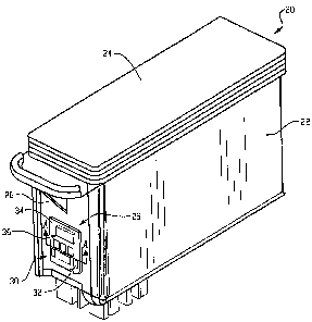
[0023] With reference now to FIGURE 2, an ink cartridge 20 is shown. The
cartridge
is adapted for mounting with an associated ink jet printing apparatus (not
shown). The
cartridge 20 includes a container 22 having an inner surface (not shown)
defining a
chamber for holding ink or other marking material therein, and a!id 24. In
accordance
with the invention, a single-sided rigid printed circuit board 30 is disposed
in a receiving
area 25 on a front outer face side 26 of the cartridge 20. In the embodiment
illustrafied,
the printed circuit board 30 carries a plurality of electrical contacts 32 on
a first side 34
thereof, and an electronic device 36 mounted directly to the first side 34. It
is to be
appreciated that, in accordance with the present invention, both the
electronic device 36
as well as the plurality of electrical contacts 32 are carried on a single
first side 34 of the
printed circuit board 30. When the cartridge 20 is mounted into the associate
printing
apparatus, a controller (not shown) in the printing apparatus is electrically
connected to
the electronic device 36 through the plurality of electrical contacts 32
arranged on the
first side surface 34 of the printed circuit board 30.
[0024] FIGURE 2a is a cross-sectional view taken along line A-A of Figure- 2
illustrating a first alternative embodiment for mounting the printed circuit
board 30 on the
front face side 26 of the ink cartridge 20. In the embodiment illustrated, the
printed
CA 02588407 2007-05-17
WO 2006/055763 PCT/US2005/041788
-5-
circuit board 30 is mounted directly in abutment with the front face side 26
of the ink
cartridge 20 using a layer of a suitable adhesive 27 such as epoxy orthe like.
Figure 2b
shows a further alternative embodiment for mounting the printed circuit board
30 to the
front face side 26 of the ink cartridge 20 by means of a pair of spaced apart
"L" shaped
finger members 21, 23 defining opposing slots 29, 31 adapted to slidingly
receive
opposite edges of the printed circuit board and carry the printed circuit
board relative to
the housing. Other alternative equivalent embodiments for mounting the printed
circuit
board to the ink cartridge are also possible such as, for example, providing a
slot or
groove in the housing body and positioning at least one edge of the circuit
board in the
slot or groove with the board extending substantially perpendicularly from a
side of the
cartridge.
[0025] FIGURE 3a is a perspective view of the first side 34 of the printed
circuit
board 30 while Figure 3b shows a second or back side 38 of the printed circuit
board
30.
[0026] In accordance with the present invention, the printed circuit board 30
is a
single-sided rigid printed circuit board. In the first embodiment illustrated,
the circuit
board carries the electronic device 36 as well as the plurality of electrical
contacts 32
directly on the first side 34 of the board.
[0027] In another embodiment to be described below, the electronic device is
received in a socket directly on the first side of the printed circuit board.
[0028] FIGURE 3b shows that none of the electrical components are disposed on
the second or rear side 38 of the printed circuit board 30. A plurality of
electrical traces
40 are disposed on the first side 34 of the printed circuit board for
connecting the
electronic device 36 to the plurality of electrical contacts 32 for electrical
communication
with the associated printing apparatus (not shown) when the subject ink
cartridge 20 is
mounted therein. With continued reference to Figures 3a and 3b, the preferred
single-
sided rigid printed circuit board 30 selectively includes at least one
locating through hole
42 and a concave portion 44 for use in assisting the positioning of the single-
sided
printed circuit board 30 onto the front face side 26 of the container 22
during
manufacture. In Figure 3a, the electronic device 36 is a programmable
microcontroller
50 including a processor and a memory unit (not shown).
[0029] FIGURES 4a and 4b illustrate an alternative embodiment of the preferred
single-sided rigid printed circuit board 30' formed in accordance with another
aspect of
the invention. As shown there, the single-sided printed circuit board 30'
includes an
CA 02588407 2007-05-17
WO 2006/055763 PCT/US2005/041788
-6-
electronic device 36' disposed on a front side 34 of the printed circuit board
and in.
electrical communication with a plurality of electric contacts 32'through a
corresponding
set of electronic traces 40'. As with the first preferred embodiment described
above, the
second or back side 38' of the printed circuit board 30' is void of any
(includes no)
electronic or electrical components, thus reducing the cost of the single-
sided printed
circuit board. At least one locating through hole 32' and a concave portion
44' are
selectively provided for enabling easy positioning of the printed circuit
board 30' on the
front face side 26 of the ink cartridge 20 during manufacture. In Figures 4a
and 4b, the
electronic device 36 is preferably an application specific integrated circuit
(ASIC) chip
52 although any other integrated circuit devices can be used.
[0030] FIGURES 5a and 5b illustrate a further embodiment of the preferred
single-
sided rigid printed circuit board 30" formed in accordance with another aspect
of the
invention. As shown there, the single-sided printed circuit board 30" includes
an
electronic device 36" disposed on a front side 34" of the printed circuit
board and in
electrical communication with a plurality of contacts 32" through a
corresponding set of
electronic traces 40". In this embodiment, the electronic device 36" is
received in an
integrated circuit (IC) socket 33. The socket 33 can take on any form
including PQFP,
dual-in-line, PLCC, pin grid array, surface mount, or the like in accordance
with the
characteristics of the electronic device 36". As with the first preferred
embodiment
described above, the second or back side 38" of the printed circuit board 30"
is void of
any electronic or electrical components, thus reducing the cost of the single-
sided
printed circuit board. At least one locating through hole 32" and a concave
portion 44"
are selectively provided for enabling easy positioning of the printed circuit
board 30" on
the front face side 26 of the ink cartridge 20 during manufacture. In FIGURES
5a and
5b, the electronic device 36" is preferably a programmable microcontroller 50'
including
a processor and a memory unit (not shown).
[0031] FIGURE 6 is a cross-sectional view of the subject ink cartridge 20
carrying a
single-sided rigid printed circuit board 30 on a front face surface 26
thereof. As shown,
the printed circuit board 30 carries one or more of an electronic device 36
and a plurality
of electrical contacts 32 for interfacing the electronic device 36 with an
associated
printing apparatus (not shown). As.illustrated, the rigid single-sided printed
circuit board
30 has a fiat back side 38 adapted to directly engage and interface with the
front face
26 of the ink cartridge body 22. This reduces the overall space required for
mounting
the ink cartridge 20 into the associated printing apparatus. Preferably,
substantially the
CA 02588407 2007-05-17
WO 2006/055763 PCT/US2005/041788
-7-
entire surface of the flat back side 38 of the printed circuit board 30 is
held in contact
with the flat surface area 26 of the receiving area 25 using a suitable
mechanical
connection such as welded tabs, an adhesive material, or the like.
[0032] FIGURES 7a-7h show alternative embodiments of the subject rigid single-
sided printed circuit board used in conjunction with an ink or toner cartridge
in
accordance with the invention. It is to be appreciated that Figures 7a-7h show
only the
front face of the single-sided printed circuit board and that the back face of
each of the
embodiments illustrated in the Figures is as shown in Figures 3b, 4b or 5b.
[0033] The invention has been described with reference to the preferred
embodiments. Obviously, modifications and alterations will occur to others
upon
reading and understanding the preceding detailed description. It is intended
that the
invention be construed as including a!l such modifications and alterations
insofar as
they come within the scope of the appended claims or the equivalents thereof.
As an
example, the substantially rigid circuit board can be mounted to any of a
variety of
devices carrying or storing consumable materials such as, for example, toner
cartridges,
paint or other marking material containers, chemical storage devices and
consumer or
commercial products or devices.