Note: Descriptions are shown in the official language in which they were submitted.
CA 02588585 2007-05-24
WO 2006/065887
PCT/US2005/045215
METHOD AND APPARATUS FOR BIAS AND ALIGNMENT
CONTROL IN AN OPTICAL SIGNAL TRANSMITTER
Technical Field
The present application relates to the optical transmission of information
and,
more particularly, to a method and apparatus for bias and alignment control in
an optical
signal transmitter.
Background
Very long optical fiber transmission paths, such as those employed in undersea
or
transcontinental terrestrial lightwave transmission systems, are subject to
decreased
performance due to a host of impairments that accumulate along the length of
the optical
fiber in the transmission path. The source of these impairments within a
single data
channel includes amplified spontaneous emission (ASE) noise generated in
Erbium-
Doped Fiber-Amplifiers (EDFAs), nonlinear effects caused by dependence of the
single-
mode fiber's index on the intensity of the light propagating through it, and
chromatic
dispersion which causes different optical frequencies to travel at different
group
velocities. In addition, for wavelength division multiplexed (WDM) systems,
where
several optical channels are on the same fiber, crosstalk between channels
caused by the
fiber's nonlinear index can be problematic.
Distortions of the received waveform are influenced by design of the
transmission
line, as well as the shape of the transmitted pulses. Known long-haul systems
have been
implemented using On-Off-Keying (00K), wherein the transmitted pulse is turned
on
and off with the ones and zeros of a data bit stream. On-Off-Keying may be
implemented in a variety of well-known formats, such as Return-to-Zero (RZ),
Non-
Return to Zero (NRZ) and Chirped-Return-to-Zero (CRZ) formats. Generally, in a
RZ
format the transmitted optical pulses do not occupy the entire bit period and
return to
zero between adjacent bits, whereas in a NRZ format the optical pulses have a
constant
value characteristic when consecutive binary ones are sent. In a chirped
format, such as
CRZ, a bit synchronous sinusoidal phase modulation is imparted to the
transmitted
pulses.
CA 02588585 2007-05-24
WO 2006/065887
PCT/US2005/045215
Phase Shift Keying (PSK) is another modulation method known to those of
ordinary skill in the art. In PSK modulation ones and zeros are identified by
phase
differences or transitions in the optical carrier. PSK may be implemented by
turning the
transmitter on with a first phase to indicate a one and then with a second
phase to
indicate a zero. In a differential phase-shift-keying (DPSK) format, the
optical intensity
of the signal may be held constant, while ones and zeros are indicated by
differential
phase transitions. DPSK modulation formats include RZ-DPSK, wherein a return-
to-
zero amplitude modulation is imparted to a DPSK signal, and CRZ-DPSK.
It has been recognized that the RZ-DPSK modulation format has particular
advantages over other formats in WDM long-haul optical systems. For example,
compared to 00K, RZ-DPSK modulation provides a significant reduction in the
required
optical signal-to-noise (OSNR) for a particular bit error rate (BER). As such,
systems for
imparting a RZ-DPSK modulation to WDM optical signals have been developed.
A RZ-DPSK modulation may be applied to a signal by imparting a periodic RZ
intensity modulation to a continuous wave optical signal, and then imparting a
NRZ
DPSK data modulation to the intensity modulated signal. The order of the RZ
and DPSK
modulation may be reversed. Those of ordinary skill in the art will recognize
that the RZ
intensity modulator and the NRZ DPSK data modulator may be Mach-Zehnder-type
optical modulators. Known two-stage Mach-Zehnder type optical modulators
conduct
modulation in a two-staged manner through serially connected Mach-Zehnder type
optical modulators disposed on a single substrate, such as lithium niobate
(LN). RZ-
DPSK modulation may be generated by selecting appropriate driving voltages and
bias
points for the serially connected Mach-Zehnder modulators.
Stable and accurate setting of the Mach-Zehnder bias points is necessary to
achieve a RZ-DPSK modulated signal that results in optimal system BER. In a RZ-
DPSK signal, the modulator imparting the RZ modulation may be biased at the
peak of
the modulator transfer function, and the modulator imparting the NRZ DPSK
modulation
may be biased at the null of the transfer function. However, factors including
temperature and aging can cause the modulator transfer function to vary,
thereby
modifying the bias point necessary to achieve optimum performance. Bias
control loops
have been developed in an attempt to ensure accurate modulator biasing. Known
bias
2
CA 02588585 2013-10-02
52601-7
control loop configurations have, however, incorporated expensive and/or
inefficient
configurations.
In addition, optimum performance requires stable and accurate relative
alignment between the RZ modulator and the NRZ DPSK modulator. Optimally, the
peak
amplitude point of the RZ modulation is aligned with the center of the data
bits modulated on
the signal by the NRZ DPSK modulator. The alignment may be achieved by
delaying the
RZ modulation relative to the DPSK modulation using an electrical phase
shifter/delay circuit
coupled to the RZ modulator's drive signal. The optimal setting of the phase
shifter to
achieve proper alignment can also vary with temperature and aging. In an
attempt to address
this problem, transmitters have been configured with predetermined alignment
settings for
various temperatures. This solution, however, requires a complicated and time
consuming
factory calibration procedure, and does not account for drift in clock-data
alignment
associated with aging or modulator operating point changes.
There is therefore a need for a system and method for efficiently and reliably
controlling the modulator bias points and timing alignment in a RZ-DPSK
transmitter.
Summary
According to one aspect of the present invention, there is provided an
apparatus for transmitting an optical signal, said apparatus comprising: a
modulator for
modulating data on an optical signal with a modulation format having a
periodic intensity
modulation and a differential phase shift keying (DPSK) data modulation, said
modulator
comprising a Mach-Zehnder RZ modulator for imparting said periodic intensity
modulation in
response to a RZ bias signal, and a Mach-Zehnder NRZ modulator for imparting
said DPSK
data modulation in response to a NRZ bias signal; a phase shifter for
selectively aligning said
periodic intensity modulation and said data modulation in response to a phase
bias signal; a
low speed photo-detector, said low speed photo-detector having a bandwidth of
at least one
order of magnitude less than a data rate of said data and being configured to
detect light
scattered at an output of said NRZ modulator and provide an output
representative of power in
said light scattered at said output of said NRZ modulator; and a controller
for providing at
3
CA 02588585 2013-10-02
52601-7
least one of said RZ bias signal, said NRZ bias signal, or said phase bias
signal, in response to
said output of said low speed photodetector.
According to another aspect of the present invention, there is provided an
apparatus for transmitting an optical signal, said apparatus comprising: a
modulator for
modulating data on an optical signal with a modulation format having a
periodic intensity
modulation and a differential phase shift keying (DPSK) data modulation, said
modulator
comprising a Mach-Zehnder RZ modulator for imparting said periodic intensity
modulation in
response to a RZ bias signal, and a Mach-Zehnder NRZ modulator for imparting
said DPSK
data modulation in response to a NRZ bias signal; a phase shifter for
selectively aligning said
periodic intensity modulation and said data modulation in response to a phase
bias signal; a
low speed photo-detector, said low speed photo-detector having a bandwidth of
at least one
order of magnitude less than a data rate of said data and being configured to
detect light
scattered at an output of said NRZ modulator and provide an output
representative of power in
said light scattered at said output of said NRZ modulator; and a controller
for providing said
RZ bias signal, said NRZ bias signal, and said phase bias signal in response
to said output of
said low speed photodetector, said RZ bias signal comprising a low frequency
RZ bias dither,
said NRZ bias signal comprising a low frequency NRZ bias dither, and said
phase bias signal
comprising a low frequency phase bias dither, each of said RZ bias dither,
said NRZ bias
dither, and said phase bias dither having an associated frequency at least one
order of
magnitude less than said data rate, said controller being configured to
provide said RZ bias
signal in response to a RZ bias error value obtained by mixing a signal
representative of said
output of said photodetector with a signal representative of said la bias
dither, said controller
being configured to provide said NRZ bias signal in response to a NRZ bias
error value
obtained by mixing said signal representative of said output of said
photodetector with a
signal representative of said NRZ bias dither, and said controller being
configured to provide
said phase bias signal in response to a phase bias error value obtained by
mixing said signal
representative of said output of said photodetector with a signal
representative of said phase
bias dither.
According to still another aspect of the present invention, there is provided
a
method of operating a modulator for modulating data on an optical signal with
a modulation
3a
CA 02588585 2013-10-02
52601-7
format having a periodic intensity modulation and a differential phase shift
keying (DPSK)
data modulation, said modulator comprising a Mach-Zehnder RZ modulator for
imparting
said periodic intensity modulation in response to a RZ bias signal, and a Mach-
Zehnder NRZ
modulator for imparting said DPSK data modulation in response to a NRZ bias
signal, and
having a phase shifter coupled thereto for selectively aligning said periodic
intensity
modulation and said data modulation in response to a phase bias signal, said
method
comprising: detecting power in light scattered at an output of said modulator
using a low
speed photo-detector, said low speed photo-detector having a bandwidth of at
least one order
of magnitude less than a data rate of said data and being configured to
provide an output
representative of power at said output of said modulator; and providing at
least one of said
phase bias signal, said RZ bias signal, or said NRZ bias signal in response to
said output of
said low speed photodetector.
Brief Description of the Drawings
Reference should be made to the following detailed description which should
be read in conjunction with the following figures, wherein like numerals
represent like parts:
FIG. 1 is a simplified block diagram of one exemplary embodiment of a system
consistent with the present invention;
FIG. 2 is a simplified block diagram of one exemplary embodiment of a system
consistent with the present invention;
FIG. 3 is a simplified block diagram of a system consistent with the present
invention including an exemplary controller consistent with the present
invention;
FIG. 4 is a timing diagram showing exemplary waveforms associated with an
exemplary transmitter consistent with the invention;
FIG. 5 shows plots of Q penalty vs. RZ error signal established by a
controller
consistent with the invention;
3b
CA 02588585 2007-05-24
WO 2006/065887
PCT/US2005/045215
FIG. 6 shows plots of Q penalty vs. NRZ error signal established by a
controller
consistent with the invention;
FIG. 7 shows plots of Q penalty vs. Phase error signal established by a
controller
consistent with the invention; and
FIG. 8 is a block flow diagram illustrating an exemplary alarm bias and
alignment
control process performed by a controller consistent with the present
invention.
Detailed Description
FIG. 1 is a simplified block diagram of one exemplary embodiment of a WDM
transmission system 100 consistent with the present invention. The
transmission system
serves to transmit a plurality of optical channels over an optical information
path 102
from a transmitting terminal 104 to one or more remotely located receiving
terminals
106. Those skilled in the art will recognize that the system 100 has been
depicted as a
highly simplified point-to-point system form for ease of explanation. For
example, the
transmitting terminal 104 and receiving terminal 106 may, of course, both be
configured
as transceivers, whereby each may be configured to perform both transmitting
and
receiving functions. For ease of explanation, however, the terminals are
depicted and
described herein with respect to only a transmitting or receiving function. It
is to be
understood that a system and method consistent with the invention may be
incorporated
into a wide variety of network components and configurations. The illustrated
exemplary
embodiments herein are provided only by way of explanation, not of limitation.
In the illustrated exemplary embodiment, each of a plurality of transmitters
TX1,
TX2 . . . TXN receives a data signal on an associated input port 108-1, 108-2
... 108-N,
and transmits the data signal on associated wavelength Xi, 2. . . A. One or
more of the
transmitters TX1, TX2 . . . TXN may be configured to modulate data on the
associated
wavelength with a RZ-DPSK modulation format while providing bias and/or
alignment
control in a manner consistent with the present invention. The transmitters,
of course,
are shown in highly simplified form for ease of explanation. Those skilled in
the art will
recognize that each transmitter may include electrical and optical components
configured
for transmitting the data signal at its associated wavelength with a desired
amplitude and
modulation.
4
CA 02588585 2007-05-24
WO 2006/065887
PCT/US2005/045215
The transmitted wavelengths or channels are respectively carried on a
plurality of
paths 110-1, 110-2...110-N. The data channels are combined into an aggregate
signal on
optical information channel 102 by a multiplexer or combiner 112. The optical
information channel 102 may include optical fiber waveguides, optical
amplifiers, optical
filters, dispersion compensating modules, and other active and passive
components.
The aggregate signal may be received at one or more remote receiving terminals
106. A demultiplexer 114 separates the transmitted channels at wavelengths ki,
X2. = = XN
onto associated paths 116-1, 116-2...116-N coupled to associated receivers
RX1,
RX2...RXN. One or more of the receivers RX1, RX2...RXN may be configured to
demodulate a RZ-DPSK modulated signal and provide an associated output data
signal
on an associated output path 118-1, 118-2, 118-3, 118-N.
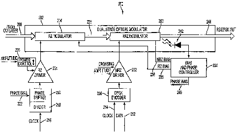
Turning to FIG. 2, there is illustrated an exemplary transmitter 200
consistent
with the present invention. The illustrated exemplary embodiment includes a
dual-stage
optical modulator 202, e.g. an LN modulator, including an RZ Mach-Zehnder type
modulator 204 for imparting a periodic RZ intensity modulation and a NRZ Mach-
Zehnder type modulator 206 for imparting an NRZ (DPSK) modulation to the
intensity
modulated signal. The two-stage modulator 202 may be driven in a known manner
to
modulate data onto a continuous wave optical signal 208, e.g. from a laser
source, with a
RZ-DPSK modulation format.
For example, the RZ modulator 204 may be driven in a well-known manner by
the data clock to impart a periodic intensity modulation to the CW optical
signal 208. As
shown, the data clock may be provided to a known divider 218 which provides an
output
including a train of identical sinusoidal pulses at half the data clock
frequency. In one
exemplary embodiment, the divider may receive a 12 GHz data clock signal and
output a
6GHz drive signal.
The output of the divider 218 may be provided to a known electrical phase
shifter/delay circuit 220. The phase shifter 220 may be configured to impart a
timing
delay to the output of the divider 218 for purposes of adjusting the alignment
of the RZ
modulation to the NRZ (DPSK) data modulation. Optimal performance is achieved
when the peak amplitude point of the RZ modulation is aligned with the center
of the
data bits modulated on the signal by the NRZ (DPSK) modulator 206. The timing
delay
5
CA 02588585 2013-10-02
52601-7
imparted by the phase shifter may be controlled by a Phase bias 222 input to
the phase
shifter 220.
The output of the phase shifter 220 may be coupled to an RF driver 224 for
driving the RZ modulator 204. The nonlinear switching characteristic of the RZ
modulator 204 doubles the frequency of the electrical drive signal from the RF
driver
224, as is well known in the art, to impart the periodic intensity modulation
to the optical
signal at a frequency equal to the data rate. The intensity modulated signal
228 is
provided at an output of the RZ modulator 204. A power control mechanism 226
may be
coupled to the RF driver 224. The power control mechanism may be configured to
adjust
the intensity modulation depth imparted to optical information signal 208. The
depth of
modulation imparted by the RZ modulator 204 may be controlled by an amplitude
control signal provided to the power control mechanism 226. In an RZ-DPSK
format the
modulation depth may be set to 100%. Periodic intensity modulation may,
however, be
imparted to the CW optical signal 208 at other modulation depths, as
described, for
example in U.S. Patent No. 6,556,326 (the '326 patent) to Neal S. Bergano.
The NRZ modulator 206 may be driven to impart a DPSK modulation to the
intensity modulated optical signal 228 in a well-known manner. As shown, for
example,
a data stream and clock may be coupled to a known DPSK encoder 230. The output
of
the DPSK encoder 230 may be provided to an RF driver 232. The RF driver 232
may
drive the NRZ modulator 206 in response to the DPSK encoder 230 output to
modulate
the phase of the intensity modulated optical signal 228 in accordance with a
DPSK
modulation format, i.e. with ones and zeros indicated by differential phase
transitions in
the optical signal. The output 244 of the NRZ modulator 206 is provided as the
modulator 202 output and is a RZ-DPSK formatted optical signal. The modulation
amplitude and the phase transition crossing point associated with the NRZ
modulator
may be adjusted using amplitude and crossing inputs to the RF driver 232.
Those of ordinary skill in the art will recognize that stable and accurate
setting
of the Mach-Zehnder modulator DC bias points and of the alignment of the RZ
modulation to the data modulation are necessary to achieve a RZ-DPSK modulated
signal that results in optimal system BER. In the illustrated exemplary
embodiment, the
6
CA 02588585 2007-05-24
WO 2006/065887
PCT/US2005/045215
modulator bias points and the alignment of the RZ modulation to the data
modulation are
established and controlled by a bias and phase controller 234. The controller
234
provides an RZ Bias output 236 to establish the DC bias of the RZ modulator
204, an
NRZ Bias output 238 to establish the DC bias of the NRZ modulator 206, and a
Phase
Bias output 240 to the Phase Bias input 222 of the phase shifter to establish
timing
alignment between the RZ 204 and NRZ 206 modulators.
As is known, optical power from the two arms of a Mach-Zehnder modulator is
coupled to the output of the modulator Y-branch as the modulator output.
Optical power
from the two arms is also scattered/radiated at or near the Y-branch coupler
and does not
appear at the modulator output. As used, herein "scattered light" and "light
scattered" at
the output of a modulator, or by a modulator, shall refer to the optical power
from the
two arms of a modulator that is scattered/radiated at or near the modulator Y-
branch
coupler.
In general, the controller bias outputs are established by the controller 234
in
response to changes of the average power in the scattered light at the output
of the NRZ
modulator 206 when dithering the modulator bias settings. The controller 234
amplifies,
low pass filters and samples the current generated by a photodetector 242,
e.g. a
photodiode, and mixes these samples separately with each dither signal to
obtain an error
value representing the energy in the photodetector current at each of the
dither
frequencies. The presence of energy at a particular dither frequency indicates
that its
associated bias voltage is not optimum. The error values are used to establish
new
associated bias settings. Optimum bias settings may be achieved by minimizing
the
associated error values.
In the illustrated exemplary embodiment, the average power in the light
scattered
by the NRZ modulator 206 is derived from the output of the photodetector 242,
which is
positioned in close proximity to the modulator Y-branch for detection of at
least a
portion of the light scattered at the output of the NRZ modulator. In one
embodiment,
the photodetector 242 may be integrated into the dual-stage modulator package
It has
been recognized that use of a photodetector which monitors the light
transmitted by the
modulator, as opposed to the scattered light, can cause the RZ bias control
loop to fail at
7
CA 02588585 2007-05-24
WO 2006/065887
PCT/US2005/045215
a specific RZ modulation depths. Using a scattered light photo-detector 242
reduces or
eliminates this problem since a much different pulse shape is imparted to the
detector.
FIG. 3 illustrates an exemplary embodiment of a bias and phase (modulation
alignment) controller 234a consistent with the invention coupled to a dual
stage
modulator 202. In operation, the controller 234a establishes initial bias
settings, Phase
Bias Setting, RZ Bias Setting, and NRZ Bias Setting, and applies low frequency
dither
signals Phase Dither, RZ Dither, NRZ Dither, respectively, to the settings.
The Phase
Bias Setting is added to the Phase Dither signal and provided to the phase
shifter as the
Phase Bias output 240 of the controller for aligning the relative phase of the
RZ
modulator 204 to the NRZ modulator 206. The RZ Bias Setting is added to the RZ
Dither signal and provided to the RZ modulator 204 as the RZ Bias output 236
of the
controller for setting the RZ modulator bias point, and the NRZ Bias Setting
is added to
the NRZ Dither signal and is provided as a NRZ output 238 of the controller to
the NRZ
modulator 206 for setting the NRZ modulator bias point. The controller 234a
adjusts the
bias settings, Phase Bias Setting, RZ Bias Setting, and a NRZ Bias Setting, in
response to
associated error values derived from comparing the average power in the light
scattered
by the NRZ modulator 206 with the dither signals.
The illustrated exemplary controller 234a generally includes an amplifier 300,
a
low pass filter (LPF) 302 and amplifier 304 coupled to the output of the
amplifier 300, a
digital signal processor (DSP) 306 including an analog-to-digital converter
(ADC) 308,
and a digital-to-analog converter (DAC) 310. As shown, the current output 312
of the
scattered photodetector 242 may be coupled to the amplifier 300. A variety of
amplifier
configurations are known to those of ordinary skill in the art. In one
embodiment, the
amplifier 300 may be configured as a logarithmic trans-impedance amplifier. A
logarithmic trans-impedance amplifier allows the ADC and associated circuitry
to
operate correctly over a wide dynamic range of monitored photocurrents.
The output of the amplifier 300 may be provided to the low pass filter (LPF)
302
and amplifier 304 configured to output an analog signal PAC containing dither
signals
recovered by the photodetector 242, plus their harmonics and noise. In an
embodiment
wherein the amplifier 300 is configured as a linear amplifier, the output of
the amplifier
300 may be provided to a second low pass filter 314 and amplifier 316
configured to
8
CA 02588585 2007-05-24
WO 2006/065887
PCT/US2005/045215
provide an analog signal Ppc, representative of the DC content of the
monitored
photocurrent. The Ppc signal may be digitized by the ADC 308, and sampled by
the DSP
306, e.g. only once for each iteration of the control loop, to achieve a value
representative
of the average power. The average power value derived from Ppc may be used to
normalize the error values to ensure that the error values increase only when
the
associated bias setting moves in the wrong direction.
The digitized PAC signal is sampled by the DSP 306. To simplify processing,
the
sampling may be conducted synchronously with the generation of the three
dither signals
Phase Dither, RZ Dither, NRZ dither. The PAC samples are mixed (i.e.
multiplied) with
each of the three generated dither tones Phase Dither, RZ Dither, NRZ dither.
The result
of each mixing is a signed error value which represents an error associated
with each bias
setting, e.g. mixing of Phase Dither with the samples produces an error value
representing error in the Phase Bias Setting, mixing of RZ Dither with the
samples
produces an error value representing error in the RZ Bias Setting, and mixing
of NRZ
Dither produces an error value representing error in the NRZ Bias Setting.
Each of the signed error values may be coupled to a separate associated
proportional-integral-differential controller (ND). Each HD may calculate new
values
for an associated one of the bias settings. The PID controllers may be
implemented in
the DSP 306, e.g. in software, hardware or a combination thereof. The DSP 306
may
provide the new control setting values via a DAC interface 318 to the DAC 310,
e.g. an
SPI bus, which produces the new bias settings. The new bias settings, Phase
Bias
Setting, RZ Bias Setting, and NRZ Bias Setting provided by the DAC 310 may be
added
to their associated dither signals, Phase Dither, RZ Dither, NRZ dither,
respectively, e.g.
by adders 320, 322, 324 and coupled to the phase bias port of the phase
shifter, the bias
port of the RZ modulator, and the bias port of the NRZ modulator,
respectively.
FIG. 4 is a timing diagram showing exemplary PAC, RZ Dither, NRZ Dither,
Phase Dither and sampling instants associated with an exemplary bias and phase
controller consistent with the present invention. In a controller consistent
with the
present invention, the dither signals may be low frequency signals. As used
herein, the
term "low frequency" refers to a frequency that is at least an order of
magnitude (i.e. a
factor of 10) less than the modulator data rate. The term "low speed", as used
herein,
9
CA 02588585 2007-05-24
WO 2006/065887 PCT/US2005/045215
refers to a device having an operating bandwidth that is at least an order of
magnitude
(i.e. a factor of 10) less than the modulator data rate. Use of low frequency
dither
signals, allows use low frequency/low speed components, e.g. the scattered
light
photodetector 242, amplifier 300, LPF 302, ADC 308, DSP 306, DAC 310, etc.
capable
of manipulating and/or processing the dither signals. This reduces the cost
and
complexity of the system compared to high frequency (bandwidth on the order of
the data
rate) designs.
The PAC signal 400 shown in FIG. 4 is an analog signal. PAC is digitized by
the
ADC 308 and sampled N times by the DSP 306 for each iteration of the control
loop. In
one embodiment, a 60 KHz sampling frequency may be used to provide 60 samples
(N=60) for each iteration of the control loop. The PAC samples are multiplied,
separately,
by the RZ Dither 402 , NRZ dither 404 and Phase Dither 406 signals to obtain
separate
error values associated with the RZ bias, NRZ bias, and Phase bias,
respectively.
To avoid interference between the RZ Bias, NRZ Bias and Phase Bias control
loops, each dither signal may have a different frequency. In an embodiment
including a
60 kHz sampling frequency, the RZ dither frequency may be about 5 kHz, the NRZ
dither frequency may be about 3 kHz, and the Phase dither frequency may be
about 2
kHz. Those of ordinary skill in the art will recognize that a variety of other
sampling
and dither frequencies may be provided. To avoid interference between the
dither
frequencies, however, the dither frequencies may be established such the no
dither
frequency is an integer multiple of any other dither frequency, and the
period, TRz, MR.&
Tphase, respectively, of the dither signals are a factor of N.
In addition, to simplify the controller the phase of the dither signals may be
optimized with respect to the digitized PAC signal. The controller may be
configured, e.g.
through software, hardware or a combination of software and hardware, to allow
for
deterministic low frequency phase differences between the dither signals and
the
digitized PAC signal. The optimal phase value for,each dither signal may be
determined
by purposefully misadjusting the bias signals and measuring the error values
as a
function of the phase value. The phase value may be set for each loop at a
value that
minimizes the error value.
CA 02588585 2007-05-24
WO 2006/065887
PCT/US2005/045215
Consistent with the present invention, the optimal setting for the RZ bias,
NRZ
bias and Phase bias signals may be achieved by minimizing the associated
signed error
values. FIGS 5-7, for example, illustrate the Q penalty vs. error signal value
associated
with one exemplary controller consistent with the invention wherein the RZ
pulse width
is characterized by a carrier-to-side-band ratio (CSR) of 7.5 dB. The
illustrated Q
penalty represents the decrease in Q associated with incorrect biasing
compared to the Q
achieved with optimal biasing, i.e. a Q penalty of 0 dB represents optimal
biasing. FIG.
5 includes a plot 500 of Q penalty vs. the RZ error signal value established
by the
controller. FIG. 6 includes a plot 600 of Q penalty vs. the NRZ error signal
value
established by the controller. FIG. 7 includes a plot 700 of Q penalty vs. the
Phase error
signal value established by the controller. As shown, for a CSR of 7.5 dB the
Q penalty
associated with the modulator bias settings is below about 0.02 dB when the
error signals
values are minimized, e.g. approximately zero.
Those of ordinary skill in the art will recognize numerous methods of
minimizing
the error signal values to achieve optimum bias settings. In one embodiment,
for
example, the error signal values may be minimized by perturbing the bias
settings to
achieve a minimum error. A new bias setting may be calculated and written to
the DAC
in response to each signed error value. The sign (+1-) of the error value may
establish a
direction of change in the associated bias signal. The bias may be changed in
any
increment. Smaller incremental changes in the bias lead to increased bias
resolution and
accuracy. In one embodiment, the bias may be changed by a constant multiple of
the
error value. The optimum bias may be achieved when the same change in the
associated
average power is achieved when the bias is changed in one direction and then
back to the
optimum as is achieved when the bias is changed in the opposite direction and
then back
to the optimum. When the optimum bias is achieved the average power no longer
contains a spectral component at the fundamental of the associated dither
frequency. The
average power may still contain spectral components at harmonics of the dither
frequency.
FIG. 8 is a block flow diagram of one example of a bias and alignment control
process 800 performed by a controller consistent with the present invention.
The block
flow diagram is illustrated with a particular sequences of steps. It can be
appreciated,
11
CA 02588585 2007-05-24
WO 2006/065887
PCT/US2005/045215
however, that the sequence of steps merely provides an example of how the
general
functionality described herein can be implemented. Further, each sequence of
steps does
not have to be executed in the order presented unless otherwise indicated.
In the exemplary embodiment illustrated in FIG. 8, the process starts 802 with
initializing 804 each bias control loop. The initialization may include
setting the RZ Bias
Setting, NRZ Bias Setting and Phase Bias Setting values to levels located at
the middle
of the bias ranges, and activating the RZ Dither, NRZ Dither, and Phase Dither
signals.
The RZ Bias Setting, NRZ Bias Setting and Phase Bias Setting may be written to
the
DAC 806. A delay 808 may be provided to allow the bias settings to settle into
the DAC
analog circuitry and appear at the DAC output for addition to the dither
signals.
Once the initial bias signals and dither signals are added and provided at the
associated ports of the RZ modulator, NRZ modulator and phase shifter, N
samples of
the PAC signal may be taken 810 by the DSP. The samples may be mixed with the
dither signals to establish the error values 812, and bias adjustments may be
calculated
814 from the error values. If the adjusted bias signals are within a
predetermined
expected range 816, they may be written to the DACS 806 and flow may continue.
Otherwise, a bias control alarm may be set 818 and flow may return to the
initialization
step 804.
There is thus provided a method and apparatus for bias and alignment control
in a
RZ-DPSK transmitter that provides stable, accurate, and efficient bias and
alignment
control. In one exemplary embodiment, the apparatus includes a dual-stage Mach-
Zehnder modulator for modulating data on an optical signal with a modulation
format
having a periodic intensity modulation and a DPSK data modulation. The
modulator
may include a Mach-Zehnder RZ modulator for imparting the periodic intensity
modulation in response to a RZ bias signal, and a Mach-Zehnder NRZ modulator
for
imparting the DPSK data modulation in response to a NRZ bias signal. A phase
shifter
may be provided for selectively aligning the periodic intensity modulation and
the data
modulation in response to a phase bias signal. A low speed photodetector may
be
configured to detect scattered light at the output of the modulator. The low
speed photo-
detector may have a bandwidth of at least one order of magnitude less than a
data rate of
the data and be configured to provide an output representative of power
scattered by the
12
= CA 02588585 2013-10-02
52601-7
N'RZ modulator. A controller may provide at least one of the RZ bias signal,
the NRZ
bias signal, or the phase bias signal, in response to the output of the low
speed
photodetector.
The embodiments that have been described herein but some of the several which
utilize this invention and are set forth here by way of illustration but not
of limitation.
Many other embodiments, which will be readily apparent to those skilled in the
art, may
be made without departing materially from the scope of the invention.
13