Note: Descriptions are shown in the official language in which they were submitted.
CA 02588701 2007-05-16
HIGH SPEED MODULAR JACK
WTTH FLEXIBLE COMPENSATION CIRCUIT
[0001] This application claims priority to provisional application number
60/747,534
entitled "HIGH SPEED MODULAR JACK" filed May 17, 2006, the entirety of which
is hereby
incorporated by reference.
Background of the Invention
[0002] The invention relates to a modular jack and, more particularly, to a
modular jack
which may be compliant with multiple communication standards and/or which
includes
improved noise compensation abilities.
[0003] The use of modular plugs and jacks for data transmission is known.
Basically, in
order to establish electrical communication and a data path between a first
and second device, the
first device may send information in the form of electrical signals out into a
cable that terminates
in a plug. The second device may include a jack. The plug and jack are
designed so as to be
easily mechanically mate-able in a male-female configuration. Once the plug
and jack are
mated, electrical members in the plug and connector engage and are
electrically mated so that
electrical information signals may travel from the first device to the second
device.
[0004] This plug and jack design is limited by the physical configuration of
the modular
plug and jack. As data transmission speeds have increased, electrical
performance relating to the
transfer of electrical signals from plug to connector, has been affected. Each
plug and jack
frequently includes multiple pairs of contacts used to communicate
information. Cross talk
between these pairs (where electrical signals in one pair affect electrical
signals in another pair)
and interference from sources exteinal to the plug-jack configuration, become
more of a factor at
CA 02588701 2007-05-16
higher speeds. In order to carry the higher speed data without signal
degradation, the plug and
connector design changed to include compensation circuitry such as that used
to balanced
impedance in transmission lines.
[0005) Standards organizations such as the Telecommunication Industry
Association and
the International Organization for Standardization publish standards regarding
performance
specifications and equipment configurations for plugs and connectors.
Different levels or
"categories" have been defined for use in twisted-pair cabling such as where a
single insulated
sheath includes two twisted wires. For example, "Category 6" jacks should be
able to handle
data communications with a frequency up to 250 MHz. More recent requirements,
e.g. Category
7, require jacks which can communicate as high as 600MHz.
[0006] Prior art Category 6 jacks typically employ the compensation circuit
near
terminals in the jack. That is, a plug having contacts mates with a jack
having contacts so that
the contacts in the plug physically touch and electrically engage with the
contacts in the jack.
The electrical signals sent from the contacts of the plug to the contacts of
the jack travel through
the contact portions of the contacts of the jack to terminals portion of the
contacts of the jack and
then those terminal portions are connected to a circuit board. The
compensation circuit in these
prior art Category 6 jacks is typically disposed near the terminal portions.
For example,
information signals may travel through the terminal portions through the
compensation circuit
and then to the circuit board. The inventors of the present invention have
performed research
and learned of the surprising discovery that movement of the compensation
circnit to a different
location yields significantly better electrical characteristics as is
discussed in more detail below.
-2-
CA 02588701 2007-05-16
[0007] An example of a prior art jack which may be used for both Category 6
and
Category 7 communications is shown in U.S. Patent 6,739,892 and is reproduced
in part, in Fig.
1. Referring to Fig. 1, a prior art connector 50 consists of a shield 52, a
dielectric housing 54, a
switch insert 56 and a circuit board sub-assembly 58. When assembled, sub-
assembly 58 is
inserted into switch insert 56, switch insert 56 is inserted into housing 54,
and housing 54 is
inserted into shield 52. When a Category 6 plug is inserted into jack 50,
terminals on sub-
assembly 58 engage corresponding terminals of the plug for data communication.
If a Category
7 plug is inserted into jack 50, a protrusion on the plug (not shown) engages
a switch 60 on
switch insert 56. Switch 60 causes some of the ternunals in connector 50 to be
lifted away from
electrical connection and moved into contact with a grounding member (not
shown).
[0008] There are problems with the prior art connector shown in Fig. 1.
Requiring a
switch to disengage or ground some of the terminals increases the complexity
of the device.
Moreover, there is the possibility of an open circuit especially if there is a
failure in the switch.
Finally, any compensation circuitry is disposed from tenninal portions of the
contacts.
Summarv of the Invention
[0009] One embodiment of the invention is a jack comprising a housing and a
contact
block in the housing, the contact block including a base member and a
plurality of contacts
carried by the base member, each contact including a contact portion effective
to touch a
corresponding contact of a plug when the plug is inserted into the jack, a
first end portion
effective to be attached to an electronic circuit, and a second end portion.
The jack further
comprises a substrate connected to the second end portion, the substrate
including a
compensation circuit for the jack.
-3-
CA 02588701 2007-05-16
[0010] Another embod'unent of the invention is a jack comprising a housing and
at least
one contact in the housing, each contact including a contact portion effective
to touch a
corresponding contact of a plug when the plug is inserted into the jack, a
first end portion
effective to be attached to an electronic circuit, and a second end portion.
The jack further
comprises a substrate connected to the second end portion, the substrate
including a
compensation circuit for the jack.
Brief Descrintion of the Drawing
[0011] Fig. 1 is a side perspective view of a jack in accordance with the
prior art.
[0012] Fig. 2 is a side perspective cut-away view of a jack in accordance with
an
embodiment of the invention.
[0013] Fig. 3 is a magnified side perspective cut-away view of a combination
plug and
jack in accordance with an embodiment of the invention.
[0014] Fig. 4 is a side perspective cut-away view of a jack in accordance with
an
embodiment of the invention.
[0015] Fig. 5 is a bottom perspective cut-away view of a jack in accordance
with an
embodiment of the invention.
[0016] Fig. 6 is a rear perspective cut-away view of a jack in accordance with
an
embodiment of the invention.
[0017] Fig. 7 is a side perspective cut-away view of a jack in accordance with
an
embodiment of the invention.
-4-
CA 02588701 2007-05-16
[0018] Fig. 8 is a side perspective cut-away view of a jack in accordance with
an
etnbodiment of the invention.
[0019] Fig. 9 is a side perspective cut-away view of a jack in accordance with
an
embodiment of the invention.
[0020] Fig. 10 is a side perspective view of a jack in accordance with an
embodiment of
the invention.
[0021] Fig. 11 is a side perspective view of a jack in accordance with an
embodiment of
the invention.
[0022] Fig. 12 is a side perspective view of a jack in accordance with an
embodiment of
the invention.
[0023] Fig. 13 is a front perspective view of a plug combined with a jack in
accordance
with an ernbodiment of the invention.
[0024] Fig. 14 is a top perspective view of a plug combined with a jack in
accordance
with an embodiment of the invention.
[0025] Fig. 15 is a front cut-away view of a jack in accordance with an
embodiment of
the invention.
[0026] Fig. 16 is a side cut-away view of a jack in accordance with an
embodiment of the
invention.
[0027] Fig. 17 is a chart detailing particular measurements which could be
used in
constructing an ernbodiment of the invention.
-5-
CA 02588701 2007-05-16
[0028] Fig. 18 is a chart detailing particular measurements which could be
used in
constructing an embodiment of the invention.
[0029] Fig. 19 is a side perspective cut-away view of a jack in accordance
with an
embodiment of the invention.
[0030] Fig. 20 is a front perspective cut-away view of a jack in accordance
with an
embodiment of the invention.
[0031] Fig. 21 is a side perspective cut-away view of a housing which could be
used in
accordance with an embodiment of the invention.
[0032] Fig. 22 is a circuit diagram along with tolerances for circuit elements
which could
be used in accordance with an embodiment of the invention.
[0033] Fig. 23 is a bottom perspective view of a jack in accordance with an
embodiment
of the invention.
[0034] Fig. 24 is a side perspective exploded view of a jack in accordance
with an
embodiment of the invention.
[0035) Fig. 25 is a front perspective view of a contact block in accordance
with an
embodiment of the invention.
[0036] Fig. 26 is a bottom perspective view of a contact block in accordance
with an
embodiment of the invention.
[0037] Fig. 27 is a rear perspective view of a jack in accordance with an
embodiment of
the invention.
-6-
CA 02588701 2007-05-16
[0038] Fig. 28 is a front perspective view of a jack in accordance with an
embodiment of
the invention.
[0039] Fig. 29 is a top perspective view of a contact block in accordance with
an
etnbodiment of the invention.
[0040] Fig. 30 is a top perspective view of a plurality of contacts in
accordance with an
embodiment of the invention.
[0041] Fig. 31 is a top view of a plurality of contacts in accordance with an
embodiment
of the invention.
[0042] Fig. 32 is a bottom perspective view of a plurality of contacts in
accordance with
an embodiment of the invention.
[0043] Fig. 33 is a bottom perspective exploded view of a jack in accordance
with an
embodiment of the invention.
[0044] Fig. 34 is a side perspective exploded view of a jack in accordance
with an
embodiment of the invention.
[0045] Fig. 35 is a front perspective view of a contact block in accordance
with an
embodiment of the invention.
[0046] Fig. 36 is a side perspective view of a jack in accordance with an
embodiment of
the invention.
[0047] Fig. 37 is a front perspective view of a jack in accordance with an
embodiment of
the invention.
-7-
CA 02588701 2007-05-16
[0048] Fig. 38 is a side perspective exploded view of a jack in accordance
with an
embodiment of the invention.
[0049] Fig. 39 is a bottom perspective exploded view of a jack in accordance
with an
embodiment of the invention.
[0050] Fig. 40 is a side perspective view of a contact block in accordance
with an
embodiment of the invention.
[0051] Fig. 41 is a rear perspective view of a contact block in accordance
with an
embodiment of the invention.
[0052] Fig. 42 is a front perspective view of a jack in accordance with an
embodiment of
the invention.
Detailed Description of the Preferred Embodiment(s)
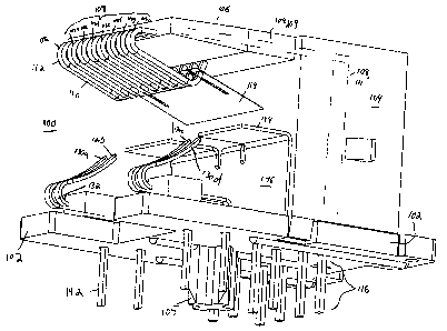
[0053] Referring to Fig. 2, there is shown a jack 100 in accordance with an
embodiment
of the invention with a portion of the housing removed. Jack 100 is capable of
communicating
with a plug (not shown) using Category 6, Category 6A, Category 7, Category 7A
communication standards as well as other communication standards. Jack 100
includes a base
102 on which elements of jack 100 are mounted. A post 105 having a cross-
shaped cross-section
extends from a bottom of base 102 and may be used to mechanically mount jack
100 to a circuit
board (not shown). Although shown on a bottom of jack 100, post 105 could be
disposed on a
top of jack 100 and used to mount jack 100 to a circuit board from either
above, below, to the
side or oblique to jack 100.
-8-
CA 02588701 2007-05-16
[0054] Jack 100 includes a pass-through housing 104 (which may include a
removable
cover having recesses) mounted on base 102. As discussed below, pass-through
housing 104
may be used to provide a pathway for tenninals to pass through to base 102.
Housing 104
includes a cantilevered support 106. Support 106 supports upper contacts 108.
As shown, eight
(8) upper contacts 108a, 108b, 108c, 108d, 108e, 108f, and 108g may be used as
is customary in
RJ45 type connectors when communicating at Category 6 or 6A speeds and
configurations.
Upper contacts 108 include contact portions 110 which physically touch
contacts of an inserted
plug (partially shown in Fig. 3). Upper contacts 108 further include an
arcuate connecting
portion 112 fixed at one end to support 106. Contact portions 110 extend
downward into a plug-
receiving area of jack 100 and terminate at first ends 114. First ends 114 are
coupled to a
flexible substrate 118 upon which a compensation circuit is provided.
[0055] Upper contacts 108 farther include bridge portions 109 that extend
through the
cantilevered support 106 (e.g. are insert molded therein), and vertical
terminal portions 111 that
extend through pass-though housing 104 and though base 102 - both shown in
dotted lines.
Upper contacts 108 exit from base 102 to form pins 116 to provide electrical
connnunication
with a circuit board (not shown). Pins 116 exit base 102 in two planes as
shown.
[0056] Flexible compensation circuitry 118 may be used to cancel out
interference
between neighboring pairs of contacts 108, reduce cross-talk between contacts
108, or to balance
a cable terniinating in jack 100. A circuit including capacitors electrically
connecting
neighboring contacts 108 may be used. For example, referring to contacts 108a-
108h as first
though eighth, respectively, between a third and a fifth contact 108, a
capacitor with a value in a
range of approximately 300 to 3600 fF could be used; between a fourth and a
sixth contact 108, a
capacitor with a value in a range of approximately 300 to 3600 fF could be
used; between a first
-9-
CA 02588701 2007-05-16
and a third contact 108, a capacitor with a value in a range of approximately
0 to 2400 fF could
be used; between a second and a sixth contact 108, a capacitor with a value in
a range of
approximately 0 to 2100 fF could be used; between a third and a seventh
contact 108, a capacitor
with a value in a range of approximately 0 to 2100 tF could be used; between a
sixth and an
eighth contact 108, a capacitor with a value in a range of approximately 0 to
2400 fF could be
used. Other arrangements and capacitance values are within the scope of the
invention.
[0057] Referring to Fig. 3, there is shown an enlarged cut - away view of the
connection
between flexible compensation circuitry 118 and contacts 108. As shown, when a
plug with a
blade-like contact 120 is inserted into jack 100, plug blade 120 physieally
touches and
communicates electrically with one of contacts 108. Flexible compensation
circuit 118 is
soldered at circuit contacts 124 to the ends of contacts 108. The connection
is designed to
minimize the distance D between the point 126 of the plug-connector contact
and the connection
of the connector contact to the circuit 118 to minimize signal degradation.
[0058] Flexible compensation circuit 118 has a flexible substrate including a
plurality of
spaced fingers 109a..109h (only 109a..109f shown in the figure). The spacing
of fingers 109
allows contacts 108 to move independently to accommodate variations in size of
an inserted
plug. If compensation circuit 118 were a solid member, contacts 108 may be
required to move
together to accommodate plug variations. When plug blades 120 engage the
contact portions 110
of contacts 108 (thereby flexing contacts 108 around arcuate portions 112),
respective fingers
109 of circuit substrate 118 will also flex andJor move to allow for such
insertion but still remain
connected to contacts 108.
-10-
CA 02588701 2007-05-16
[0059] Referring again to Fig. 2, jack 100 may be used to provide electrical
connection
with a plug using Category 6 communication. Upper contacts 108 enable such
communications.
Jack 100 further allows for communication using Category 7 speeds and
corresponding plugs.
Such plugs have blade-like contacts disposed on both a top and a bottom of the
plug. To
accommodate such plugs, jack 100 includes bottom contacts 130 on a side of
jack 100 opposite
contacts 108. As shown, four bottom contacts 130a, 130b, 130c, and 130d, are
arranged in two
pairs on a bottom ofjack 100 on a side opposite upper contacts 108.
[0060] Each bottom contact 130 includes a base portion 132 fixedly mounted to
a
mounting member 134. For simplicity, explanation will be made with respect to
bottom contact
130a though it should be clear that all bottom contacts 130 are similarly
structured. As shown
most clearly in Fig. 4 (where base 102 has been removed for clarity), mounting
member 134 has
a downwardly extending cylindrical shaped projection 136. Projection 136 may
be used to mate
with a corresponding recess in base 102. Bottom contacts 130 fiuther include
an arcuate portion
138 and terminate at a first contact portion 140. First contact portion 140 is
spring biased
upwardly at arcuate portion 138 so as to enhance electrical and mechanical
communication with
an inserted plug. Bottom contacts 130 have vertical portions which project
through the base 102
(Fig. 3) to form pins 142 which communicate with a circuit board (not shown).
Pins 142 exit
base 102 in two planes as shown.
[0061] Referring to both Figs. 2 and 4, an L-shaped shield 144 made of a
metallic
material is mounted to housing 104. Shield 144 includes a base portion 146
extending parallel to
the pins 116 of upper contacts 108 and to pins 142 of lower contacts 130.
Shield 144 further
includes a flange 148 extending perpendicular to base 146. Shield 144 includes
a tab 150
-11-
CA 02588701 2007-05-16
extending parallel to flange 148 but in an opposite direction from flange 148.
Tab 150 may be
used to mount shield 144 to housing 104 through a T-shaped recess 152 shown in
Fig. 5.
[0062] Shield 144 provides desirable shielding for connector 100 when used
with
Category 7 communications. Base 146 of shield 144 provides shielding between
bottom contacts
130 and the vertical portions 111 of top contacts 108 that extend through
through-housing 104.
Further, flange 148 provides shielding between bottom contacts 130 and top
contacts 108 in an
area where a plug is inserted into connector 100.
[0063] When using Category 7 communications, laterally disposed pairs of upper
contacts 108a, 108b, 108g and 108h are used. Referring to Fig. 6, to further
shield signal pairs in
these upper contacts from each other, a vertical shield 154 may be used to
shield
communications between upper contacts 108a, 108b and contacts 108g, 108h
(contacts shown
most clearly in Fig. 2) as the vertically extending contact portions 110 (Fig.
2) of these contacts
extend on either sides of shield 154. Of upper contacts 108, only contacts
108a, 108b, 108g and
108h are used for Category 7 communications. The vertical shield 154 may be
made of a
metallic material and may be mounted in a rear of housing 104 in a recess 156
and in a support
158. Referring also to Fig. 7, an additional vertical shield 160 may be
mounted on support 106
between upper contacts 108d and 108e. Again, shield 160 is made of a metallic
material and
serves to shield upper contacts 108a, 108b from upper contact 108g, 108h when
Category 7
communications are used. As discussed, when Category 7 communications and
plugs are used,
shields 144, 154 and 160 may be used to shield communication between
respective upper and
lower contacts 108, 130.
-12-
CA 02588701 2007-05-16
[0064] Now that the arrangement of the contacts for connecting the jack with a
plug and
the shielding of these contacts has been described, the housing and external
shielding ofjack 100
will be explained. Referring now to Fig. 8, a housing 170 of connector 100
includes a top 172, a
top front 174, a bottom front 180 and sides 178. Note that Fig. 8 is a cut-
away view of housing
170 and only one side 178 is shown. Top front 174 includes cavities 176 for
receiving optical
light pipes discussed below. Top front 174 fiuther includes a flat frame
portion 182 used to help
define an insertion area 184 for a plug (not shown) to be inserted. Bottom
front 180 of housing
170 has a stepped cross-section typical for receiving modular plugs. Flat
frame portion 182, in
combination with sides 178 and bottom front 180 define a plug-receiving cavity
184. Cavity 184
is defined so as to be capable of receiving both Category 6 and Category 7
plugs.
[0065] Referring to Fig. 9, more detail of housing 170 is shown including the
provision
of optical light pipes. As shown in the figure, optical light pipes 188 may be
inserted into a
longitudinal opening defined by housing 170. The openings terminate at ends of
housing 170
and form cavities 176 defined by top front portion 174. Each optical light
pipe 188 includes an
exposed end 186 situated in a respective cavity 176. LEDs 192 are disposed at
a rear of housing
170 and include LED terminals 194 extending downwardly. LEDs 192 are in
optical
communication with light pipes 192 so that light emitted from LEDs 192 may
travel through
light tubes 192 and be visible at ends 186. Such light may indicate that jack
100 is receiving
power and/or indicate that jack 100 is receiving or transmitting information
or simply connected
to a plug. Light pipes 188 include outwardly biased flanges 190 used to
connect light pipe 188
to housing 170. Flange 190 is discussed in more detail below. A rear support
193 is used to
retain LEDs 192 and terminals 194 on housing 170 and to provide further
structural support for
housing 170.
-13-
CA 02588701 2007-05-16
[0066] Refetring to Fig. 10, there is shown a view of the entire housing 170.
As shown,
sides 178 of housing 170 further include rear portions 196. Rear portions 196
define openings
198 for receiving the flanges 190 of light tubes 188. In this way, light tubes
188 may be inserted
from a rear of housing 170 toward front 174, 180 of housing. A user inserting
tubes 188 into
housing 170 causes outward biased flange 190 to bend inwardly. Once flange 190
of light tube
188 reaches opening 198, flange 190 again extends outwardly thereby
maintaining tube 188 in
housing 170. To replace tube 188, a user may push flange 190 inward and then
push tube 188 to
the rear of housing 170.
[0067] Referring to Figs. 11-14, there is shown an exterrnal shield 200 which
may be used
with jack 100. Shield 200 includes a base including a top portion 202, lips
204 which extend
from top 202 to sides of jack 100, side front portions 206, side rear portions
208, and a front face
218. Side front portions 206 terminate in ground connectors 210. Ground
connectors 210 may
be used to ground shield 200 to a circuit board. Shield 200 includes spring
members 212
extending outward from top 202, sides 206, 208 and a bottom 216 of shield 200.
Spring members
212 are effective to engage a grounding member (not shown) of a chassis (not
shown) when jack
100 is inserted into the chassis.
[0068] Focusing on Figs. 13 and 14, there is shown a plug 300 mating with jack
100.
These figures highlight how shield 200 of jack 100 provides grounding for an
inserted plug. A
top spring 213 (Fig. 13) of shield 200 touches a point 308 (Fig. 14) of shield
302 of plug 300.
Further, spring member 214 of shield 200 touch sides of shield 302 of plug
300. Finally, a
bottom spring 215 of shield 200 touches a bottom of shield 200. In this way,
shield 302 of plug
300 is brought to the same potential as shield 200.
-14-
CA 02588701 2007-05-16
[0069] Referring to Figs. 15-18, there are shown various dimensions for the
spacing of
contacts on Category 7 connectors. Fig. 15 is a front cut-away view of a
Category 7 connector
and Fig. 16 is a side cut-away view of Category 7 connector. Figs. 17 and 18
are charts listing
some of the preferred dimensions for the various structures though it should
be clear that other
dimensions could be used and would be within the scope of the invention.
[0070] Referring to Fig. 19, there is shown another embodiment of the
invention. In Fig.
19, a jack 100' includes many of the same components as jack 100 and a
detailed description of
these components is therefore omitted. For example, shield 154 may be used
with jack 100'.
Jack 100' includes upper contacts 108' (shown at a lower portion of the
figure) shaped differently
from upper contacts 108 of connector 100. Contacts 108' include contact
portions 230 effective
to communicate with contacts of a plug (not shown) and a base portion 232.
Base portion 232 is
captured under a lip of base portion 106'. Upper contacts 108' continue
through pass through
housing 104 and terminate at pins 116'. In this embodiment, mounting post 104
is disposed
distal from both tenninals 142 of lower contacts 130 and ternunals 116' of
upper contacts. The
use of the terms "upper" and "lower" are for convenience only and can be used
interchangeably.
For example, mounting post 104 may be used to mount connector 100 or connector
100' from
above or from below. In the embodiment of Fig. 19, all of terminals 142 and
116' from both
lower contacts 130 and upper contacts 108' emerge at the top of jack 100'. The
structures shown
for upper contacts 130 and for mounting post 104' could be used with any of
the previously
described embodiments.
[0071] Referring to Fig. 20, there is shown a more complete view of jack 100'.
As
shown, jack 100' includes an upper printed circuit board 246 from which
terminals 142 and 116'
of both lower contacts 130 and upper contacts 108' extend. Also extending from
upper circuit
-15-
CA 02588701 2007-05-16
board 246 are input terminals 240 and 242 which are in electrical
communication (circuitry not
shown) with ends 142 and 116'. Terminals 240 and 242 are connected to magnetic
filter circuits
244. Magnetic filter circuits 244 may be used to remove spurious signals
moving through jack
100' andlor may be used to remove any signal interference such as that caused
by
electromagnetic waves incident upon jack 100'. As shown, two input terminals
240 and two
input ternninals 242 are connected to respective magnetic filter circuits 244 -
i.e. there are four
magnetic filter circuits, each with its own set of cores. An output of the
magnetic filter circuits
244 is fed to output terminals 250 and 252 respectively.
[0072] Referring to Fig. 21, each magnetic filter circuit 244 is disposed in
its own filter
cavity 254. A housing divider 256 disposed on either side of connector 100'
separates and
defines these cavities. Jumper pins 258 extend away from upper circuit board
246 and are used
to provide electrical communication to magnetic filter circuits 244.
[0073] Referring to Fig. 22, there is shown an example of circuit which may be
used for
magnetic filter circuits 244. Also shown is circuitry 270 which may be used to
connect terminals
142 and 116 with input terminals 240, 242, and circuitry 272 which may be used
to connect
magnetic filter circuits 244 to output terminals 250, 252. Also shown are some
tolerances for the
circuit elements depicted. Clearly these elements and tolerances may be
changed without
altering the scope of the invention.
[0074] Referring to Fig. 23, there is shown a view of jack 100' including a
shield. As
with jack 100, jack 100' includes a shield front 260, a shield rear 262 and
grounding posts 264
used in grounding the shield to a circuit board (not shown).
-16-
CA 02588701 2007-05-16
[0075] Refening to Fig. 24, there is shown a jack 300 in accordance with
another
embodiment of the invention. Jack 300 may receive a plug inserted in a
direction perpendicular
to a plane defined by a surface of a circuit board (not shown) where jack 300
is mounted -
sometimes referred to as a "vertical jack". Jack 300 includes a contact block
302, a housing 304
and a shield 306. Referring also to Figs. 25 and 26, contact block 302
includes a base plastic
member 316 carrying contacts 317 having an arcuate portion 314, a contact
portion 312, an end
portion 310 and a tenninal end 318. Plastic member 316 further includes a
tongue 332
(discussed below). End portion 310 is connected to flexible substrate 308
including
compensation circuitry as discussed above. Contacts further include terminal
ends 318 used in
connecting with a circuit board (not shown). Base plastic member 316 may have
a central
portion cut-out (shown at 340) to reduce the dielectric constant of the base
plastic member 316
and to improve relevant electrical properties.
[0076] Housing 304 includes walls 320 defining a plug receiving cavity 324, a
mounting
post 322 used in mounting jack 300 to a circuit board (not shown), a flexible
tab 336 biased
upwardly and a groove 324. Shield 306 includes spring members 328, effective
to facilitate
grounding of jack 300, and spring biased outwardly from a base of shield 306.
Shield 306
further includes ground posts 326 and a void 338 effective to receive and
retain tab 336 of
housing 304 therein.
[0077] Referring to Figs. 24, 27 and 28, to assemble jack 300, a user may
slide tongue
332 of contact block 302 into groove 334 (Fig. 27) of housing 304 and then
insert housing 304
into shield 306 so that tab 336 mates with void 338.
-17-
CA 02588701 2007-05-16
[0078] As shown most clearly in Figs. 26 and 27, terminal ends 318 enter base
plastic
member 316 in a single plane (Fig. 26) but may move to different planes inside
plastic member
316 (as best seen through cut-away 340) and exit plastic member 316 in
different planes. As
shown in Fig. 27, terminals ends 318 may exit plastic member 316 at a first
plane 342 and a
second plane 344. Terminal ends 318a, 318b, 318c, 318f, 318g and 318h remain
in their
respective planes 342 and 344. However, temzinal ends 318d and 318e (which may
correspond
to wires 4 and 5) may optionally cross-over so that they terminate in
different planes. Terminal
ends 318 may alternatively remain in their respective planes 342, 344 as shown
in Fig. 29.
[0079] Inside plastic member 316, the contacts 317 may cross-over one another
one or
more times to reduce cross-talk between contacts. As shown in Figs. 30 and 31
(with plastic
member 316 removed for illustration), in addition to the optional cross-over
of tenminal ends
318d, 318e, contacts 317a and 317b may cross-over inside plastic member 316 at
cross-over
point 346 so that contact portions 312a, 312b terminate in terminal ends 318b
and 318a
respectively. Similarly, contacts 317d and 317e may cross-over inside plastic
member 316 so
that contact portions 312d, 312e tenninate in temzinal ends 318e and 318d
respectively; and
contacts 317g and 317h may cross-over inside plastic member 316 so th.at
contact portions 312g,
312h terminate in terminal ends 318h and 318g respectively.
[0080] Alternatively, as shown in Fig. 32, contacts 317a, 317b, may cross-over
twice at
cross-over points 346 and 348 so that contact portions 312a, 312b terminate in
terminal ends
318a, 318b. Similarly, contacts 317d, 317e, may cross-over twice so that
contact portions 312d,
312e terminate in terminal ends 318d, 318e and contacts 317g, 317h, may cross-
over twice so
that contact portions 312g, 312h terminate in terminal ends 318g, 318h.
-18-
CA 02588701 2007-05-16
[0081] Referring to Figs. 33 and 34, there is shown a jack 400 in accordance
with another
embodiment of the invention. Jack 400 may receive a plug inserted in a
direction parallel to a
plane defined by a surface of a circuit board (not shown) where jack 400 is
mounted - sometimes
refen-ed to as a "horizontal jack". Jack 400 includes a rear cover 430, a
contact block 402, a
housing 404 and a shield 406. Rear cover 430 includes recesses 450. Referring
also to Fig. 35,
contact block 402 includes a base plastic member 416 carrying contacts 417
having an arcuate
portion 414, a contact portion 412, an end portion 410 and a terminal end 418.
Plastic member
416 further includes a tongue 432 (discussed below). End portion 410 is
connected to flexible
substrate 408 including compensation circuitry as discussed above. Contacts
417 further include
terminal ends 418 used in connecting with a circuit board (not shown). Base
plastic member 416
may have a central portion cut-out to reduce the dielectric constant of the
base plastic member
416 and to improve relevant electrical properties as discussed above or may be
solid as shown in
the figure.
[0082] Housing 404 includes walls 420 defining a plug receiving cavity 424, a
mounting
post 422 used in mounting jack 400 to a circuit board (not shown), and a
groove 424. Shield 406
includes spring members 428, effective to facilitate grounding of jack 400,
and spring biased
outwardly from a base of shield 406. Shield 400 also includes a ground post
426, a flexible tab
436 biased upwardly and a void 438 effective to receive and retain tab 436
therein. A rear of
shield 406 may be opened up to receive housing 404 by disengaging tab 436 from
void 438.
[0083] Referring to Figs. 33, to assemble jack 400, a user may slide tongue
432 of
contact block 302 into groove 424 of housing 304 and then insert housing 404
into shield 406.
Rear cover 430 may then be slid on to contact block 402 with recesses 450 of
rear cover 430
mating with terminal ends 418. An assembled jack 400 is shown in Fig. 37.
-19-
CA 02588701 2007-05-16
[0084] As shown most clearly in Figs. 35 and 36, terminal ends 418 enter base
plastic
member 416 in a single plane but may move to different planes inside plastic
member 416 and
exit plastic member 416 in different planes. Terminal ends 418a, 418e, 418f,
418g may exit
plastic member 416 at a first plane 442 and terminal ends 418b, 418c, 418d,
and 418h may exit
plastic member 416 at a second plane 444. Once terminal ends 418 exit plastic
member 416,
terminal ends 418 may bend downwardly at bends 443 and 445 so as to be insert-
able in a circuit
board extending parallel to plug receiving cavity 424. As can be seen,
terminal ends 418b, 418d,
418f and 418h bend at first bends 443 and terminate in a third plane 450.
Terminal ends 418a,
418c, 418e, and 418g bend at second bends 445 and terminate in a fourth plane
452. Terminals
418c and 418f cross-over in that they start off in a plane with three
terminals and end up in a
plane with a different three terminals. Jack 400 may also use the cross-over
arrangements
discussed above with reference to Figs. 30-32.
[0085] Referring to Figs. 38 and 39, there is shown ajack 500 in accordance
with another
embodiment of the invention. Jack 500 may receive plug inserted in a direction
oblique to a
plane defined by a surface of a circuit board (not shown) where jack 500 is
mounted - sometimes
referred to as an "angle jack". Jack 500 includes a contact block 502, a
housing 504 and a shield
506. Referring also to Figs. 40 and 41, contact block 502 includes a base
plastic member 516
carrying contacts 517 having an arcuate portion 514, a contact portion 512, an
end portion 510
and a terminal end 518. Plastic member 516 further includes a tongue 532
(discussed below).
End portion 510 is connected to flexible substrate 508 including compensation
circuitry as
discussed above. Contacts 517 further include terminal ends 518 used in
connecting with a
circuit board (not shown). Base plastic member 516 may have a central portion
cut-out to reduce
-20-
CA 02588701 2007-05-16
the dielectric constant of the base plastic member 516 and to improve relevant
electrical
properties as discussed above or may be solid as shown in the figure.
[0086] Housing 504 includes walls 520 defining a plug receiving cavity 524, a
mounting
post 522 used in mounting jack 500 to a circuit board (not shown), and a
groove 524. Shield 506
includes spring members 528, effective to facilitate grounding of jack 500,
and spring biased
outwardly from a base of shield 506.
[0087] Referring to Figs. 38 and 39, to assemble jack 500, a user may slide
tongue 532 of
contact block 502 into groove 524 of housing 504 and then insert housing 504
into shield 506.
An assembled jack 500 is shown in Fig. 42.
[0088] As shown most clearly in Figs. 40 and 41, terminal ends 518 enter base
plastic
member 516 in a single plane but may move to different planes inside plastic
member 516 and
exit plastic member 516 in different planes.
[0089] Contacts 517 may exit plastic 516 at two planes 544, 542. As shown,
terminal
ends 518a, 518e, 518f, and 518g exit plastic member 516 at first plane 542 -
which is more
toward a top of plastic member 516 than a second plane 542. Conversely,
terminal ends 518b,
518c, 518d, and 518h exit plastic member 516 at second plane 544 which is more
toward a
bottom of plastic member 516 than first plane 542.
[0090] Terminal ends 518a, 518e, and 518g bend so that terminals ends 518a,
518e, and
518g terminate in a third plane 552 which is more toward a top of plastic
member 516 than a
fourth plane 550.
-21-
CA 02588701 2007-05-16
[0091] Terminal ends 518b, 518d, and 518h bend so that terminal ends 518b,
518d, and
518h terminate in fourth plane 550 which is more toward a bottom of plastic
member 516 than
third plane 552.
[0092] Terminal ends 518c and 518f cross-over in that they start off in a
plane with three
terminals and end up in a plane with a different three terminals. Jack 500 may
also use the cross-
over arrangements discussed above with reference to Figs. 30-32.
[0093] Having described the preferred embodiments of the invention, it should
be noted
that the scope of the invention is limited only by the scope of the claims
attached hereto and
obvious modifications may be made without departing from the scope and spirit
of the invention.
-22-