Note: Descriptions are shown in the official language in which they were submitted.
CA 02590062 2007-06-07
WO 2006/063037 PCT/US2005/044236
AUTOMATIC POWER FACTOR CORRECTOR
1. Field of the Invention. This invention relates to power factor
c.orrection. More specifically, this invention relates to computer controlled
solid-state
switching power factor correction.
2. Description of Related Art. A variety of techniques for power factor
correction have been proposed and are well known in the art. Generally, these
prior
systems and techniques sense only one phase and switch, using contactor
relays, all
three phases at one time.
Although, the following may not necessarily be "prior art", the reader is
referred to the following U.S. patent documents for general background
material.
Each of these patent documents is hereby incorporated by reference in its
entirety for
the material contained therein.
U.S. Patent No. 4,356,440 describes a discrete-time, closed loop power factor
corrector system that control the coupling of a delta-connected switched
capacitor array to a 3- or 4-wire power line which may have time-varying,
unbalanced, inductive loads.
U.S. Patent No. 4,417,194 describes an electric power generator system that
includes a switched capacitor controlled induction generator adapted to
provide power
at a regulated voltage and frequency.
U.S. Patent No. 4,493,040 describes a computer-controlled welding apparatus
that includes a phase-controlled resistance welding circuit for selectively
conducting
pulses of a welding current to a workpiece and a control circuit for
controlling the
conduction of the welding circuit.
U.S. Patent No. 5,134,356 describes a system and method for determining and
providing reactive power compensation for an inductive load.
U.S. Patent No. 5,180,963 describes an optically triggered solid-state switch
and method for switching a high voltage electrical current.
U.S. Patent No. 5,473,244 describes an apparatus for performing non-
contacting measurements of the voltage, current and power levels of conductive
elements such as wires, cables and the like, that includes an arrangement of
capacitive
sensors for generating a first current in response to variation in voltage of
a
conductive element.
Summary of Invention
CA 02590062 2007-06-07
WO 2006/063037 PCT/US2005/044236
2
It is desirable to provide a method and system for automatically correcting
the
power factor in an electrical power system. It is particularly desirable to
provide such
a method and system, which saves electrical energy by using solid state
switching to
eliminate current in-rush and eliminating the need for the reactors required
to handle
such current in-rush. It is also desirable to provide frequent power factor
correction to
the desired levels in a system that is automatic once installed.
Accordingly, an embodiment of this invention provides conzputer controlled
solid-state switching power factor correction.
An embodiment of this invention provides power factor correction using solid
state switches that switch at or about the zero crossing point.
Furthermore, an embodiment of this invention provides power factor
correction that senses the phase angle of the current and adds or removes
capacitors as
needed on each phase individually.
Also, an embodiment of this invention provides power factor correction that
switches multiple times per second and that uses multiple steps of correction.
An embodiment of this invention provides power factor correction that
minimizes current in-rush, thereby eliminating the required reactors
associated with
this inrush of current.
An embodiment of this invention provides power factor correction that is
automatic.
An embodiment of this invention provides power factor correction that senses
multiple phases.
Additional advantages and other novel features of this invention will be set
forth in part in the description that follows and in part will become apparent
to those
skilled in the art upon examination of the following or may be learned with
the
practice of the invention. The advantages of this invention may be realized
and
attained by means of the instrumentalities and combinations particularly
pointed out
in the appended claims. Still other advantages of the present invention will
become
readily apparent to those skilled in the art from the following description
wherein
there is shown and described the preferred embodiment of this invention,
simply by
way of illustration of one of the modes best suited to carry out this
invention. As it
will be realized, this invention is capable of other different embodiments,
and its
several details, specific circuits and method steps are capable of
modification without
CA 02590062 2007-06-07
WO 2006/063037 PCT/US2005/044236
3
departing from the invention. Accordingly, the advantages, drawings and
descriptions
should be regarded as illustrative in nature and not as restrictive.
Brief Description of Drawings
The accompanying drawings incorporated in and forming a part of the
specification, illustrate a preferred embodiment of the present invention.
Some,
although not all, alternative embodiments are described in the following
description.
In the drawings:
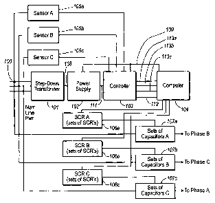
Figure 1 is a system block diagram showing the major sections of the present
embodiment of the invention.
Figure 2 is a top-level flow chart of the power factor control method of the
present embodiment of the invention.
Reference will now be made in detail to the present preferred embodiment of
the invention, an example of which is illustrated in the accompanying
drawings.
Detailed Description
Power factor correction is used to align phase angles of the voltage and
current
in an A/C power system. Power factor correction is important in maximizing the
energy efficiency of a power system. Typically power factor correction has
been
accomplished by storing unused current in capacitor(s) until the next cycle.
The use of
fixed capacitors in power factor correction has been demonstrated to have
significant
limitations in any system without constant loads. Adjustable capacitance power
correction has been attempted, but prior systems have also had significant
drawbacks.
For example, prior systems sense only one phase of a three phase electrical
system
and then "correct" all phases based only on the information from the single
phase.
Also, prior systems have typically used electro-magnetic relays, which have a
tendency to create power spikes. Electro-magnetic relays also tend to be
susceptible to
contact point wear and damage that leads to undesirable heat, resistance and
distortion. In sum, electro-magnetic relays are not appropriate for use in
switching
capacitors.
This present invention uses computerized electronic switching technology to
provide long lasting, low to no maintenance, user-friendly, full-time power
factor
correction. This invention can work with 690, 480, 308, 240 and 208 Volt three-
phase
power systems, Wye or Delta configurations and both 50Hz and 60Hz. Power
factorõ
correction from zero to maximum rating can be accomplished. This present
invention
is designed to sense the phase angle on all three phases individually and
applies to
CA 02590062 2007-06-07
WO 2006/063037 PCT/US2005/044236
4
each phase single voltage phase to current phase correction. The present
embodiment
of this invention can incrementally adjust by as little as . l7kVAr, in as
many as 256
incremental steps per phase. The number of incremental steps and amount of
adjustment can be increased or decreased in alternative embodiments of this
invention. This invention minimizes switching transients and provides true or
near-
true zero crossing through the use of computerized electronic technology.
Figure 1 shows a system block diagram showing the major sections of the
present embodiment of the invention, in this embodiment, three-phase main line
power 100 is connected to a step-down transformer 101. The three-phase main
line
power 100 can be in either a delta or Wye configuration. The step-down
transformer
101 provides 120 VAC power 108. The 120 VAC power 108 is provided to a power
supply 102. The power supply 102, in the present embodiment, provides 5 VDC
power 109 to power the controller 103 and the computer or processor 104. A
current
sensor 105a, 105b, 105c is connected to a phase of the three-phase main line
power
100, with each phase having a current sensor 105a,b,c connected thereto. The
current
sensors 105a,b,c identify the phase of the current signal being measured on
each
phase of the three-phase main line power 100. Each current sensor 105a,b,c
provides a
current signal 110a,b,c to the controller 103. A voltage signal 111 is sent
from the
power supply 102 to the controller 103. This voltage signal 111 contains the
AC
phase information of the voltage from the main line power 100. The controller
103
processes the received voltage signal 111 and the received current phase
signals
110a,b,c and produces a square wave voltage signal 112 and a square wave
current
signal 113a,b,c for each phase of the main line power 100. In this present
embodiment these signals 112, 113a,b,c are square waves, although in
alternative
envisioned embodiments these signals may be other detectable wave forms,
including
but not limited to saw-tooth waves, triangular waves, sinusoidal waves and the
like.
These signals 112, 113a,b,c are provided by the controller 103 to the computer
104
for processing. The computer 104 processes and compares the phase angle of the
signals 112, 113a,b,c. The computer 104 identifies if the phase angle of each
current
component lags or leads the phase angle of the voltage. Once the phase angle
lead or
lag, for each of the main line power phases 100 is identified by the computer
104, the
computer 104 commands banks of switches SCR A 106a, SCR B 106b and SCR C
106c to switch in or out one or more sets of capacitors 107a, 107b, 107c. In
the
present embodiment of this invention, each SCR 106a,b,c is includes eight sets
of one
CA 02590062 2007-06-07
WO 2006/063037 PCT/US2005/044236
or more SCRs, thereby, capable of switching on or off up to eight different
sets of
capacitors for each phase A, B and C. Also, in the present embodiment, each
switch
SCR A 106a, SCR B 106b, SCR C 106c is connected to a bank of eight capacitors
or
sets of capacitors 107a,b,c. Each bank of capacitors 107a,b,c is presently
composed of
5 capacitors of varying capacitance of increasing values of capacitance. For
example, a
typical bank of capacitors 107a,b,c would include a set of capacitors having a
relatively small capacitance, a second set having a value of capacitance
double that of
the first set, a third set having a value of capacitance double that of the
second set, and
so on through the eight sets of capacitors. In this manner there are up to 256
different
combinations or steps of capacitance that can be selected for each phase of
the main
line power 100. The banks of capacitance 107a,b,c each receive a single phase
of the
main line power 100 and provide three-phase power where the phase angle of the
current is aligned with the phase angle of the voltage. Accordingly, this
invention
minimizes the loss of electrical energy cause by phase differences between the
voltage
signal and the current signals. Typical AC power operates at 50 Hz or 60 Hz,
therefore in the present embodiment of this invention corrections are made by
computer 104 commands to the switches 106a,b,c to the banks of capacitors
107a,b,c,
thereby correcting the phase angles of the current and voltage signals at
least once per
cycle or 50 or 60 times per second. In alternative embodiments, the
corrections to the
phase angles of the power phases can be done more frequently or less
frequently and
required to bring the power into efficient alignment. The sensors 105a,b,c are
adapted
to sense and characterize the current components of the three-phase main line
power
100. Typically, this includes sensing the current phase angle. The controller
103
converts the sensor signals to a waveform, which can be processed and compared
by
the computer 104. The computer 104 performs the phase angle comparison and
controls the selection of capacitance for each phase of three-phase power 100.
As
noted above, the switches 106a,b,c receive the control signal from the
computer 104
and turn on or off as desired the sets of capacitors 107a,b,c in order to
effect a phase
angle shift of the current to thereby align the current with the voltage.
Figure 2 shows a top-level flow chart of the power factor control method of
the present embodiment of the invention. The present embodiment of the method
of
comparing current and voltage phase angles is performed in a programmable
computer device 104. The typical such computer 104 includes a processor;
dynamic
and static memory; a long term storage device, such as a magnetic disc drive:
an input
CA 02590062 2007-06-07
WO 2006/063037 PCT/US2005/044236
6
device, such as a keyboard and/or mouse; a display device, such as a CRT or
flat
panel display; and an output device, such as a printer or the like. Although,
in
alternative embodiments, the computer could be a stand-alone processing unit
without
dedicated input, display or output devices. Also, it is likely that the
computer device
used in this invention would be provided with a network interface for
communicating
with other computational devices, over a dedicated line, a telephone line, a
wireless
RF link or the like. The present method has been coded in the Pascal
programming
language, and has been compiled to be executed on a standard personal
computer.
Alternative embodiments of this method may be written in alternative languages
or
assembly or machine code and can be executed on special purpose computational
devices, without departing from the concept of this invention. The method
typically,
but not exclusively, begins with variable and parameter initialization 201.
The user
can then be given an opportunity to modify 202 the values and trigger points
for the
comparison between the received phase angles of the current and that of the
voltage.
A comparison 203 between the phase angle of each current with the phase angle
of
the voltage is made. If the comparison results in a difference that exceeds
the
parameter triggers or thresholds set during initialization 201 or duririg
modification
202, the SCRs are set 204 to switch either on or off the appropriate sets of
capacitors.
This comparison 203 step includes receiving the current and voltage phase
angles,
computing the difference between the current and voltage phase angles and
producing
a value for the amount of difference between the current and voltage phase
angles.
The value of difference is compared against the values and/or trigger points
initialized
in step 201 or modified in step 202. Values, including the phase angles and
other
measures of the current and voltage as well as the variables and parameters,
including
trigger points, can then be displayed 205 for the user. The process, being
continuous,
repeats 206 by returning to the modify values step 202 where the user is
provided an
opportunity to modify the values. In some alternative configurations, during
operation
the modify values step 202 and the display values step 205 would not be
performed.
These steps 202 and 205 would, in these alternative embodiments, only be
performed
during diagnostics or system administrator maintenance.
The foregoing description of the present embodiment of this invention has
been presented for the purposes of illustration and description of the best
mode of the
invention currently known to the inventor. It is not intended to be exhaustive
or to
limit the invention to the precise form disclosed. Obvious modifications or
variations
CA 02590062 2007-06-07
WO 2006/063037 PCT/US2005/044236
7
are possible and foreseeable in light of the above teachings. This embodiment
of the
invention was chosen and described to provide the best illustration of the
principles of
the invention and its practical application to thereby enable one of ordinary
skill in the
art to make and use the invention in various embodiments and with various
modifications as are suited to the particular use contemplated. All such
modifications
and variations which are within the scope of the appended claims, when then
are
interpreted in accordance with the breadth to which they are fairly, legally
and
equitably entitled, should be considered within the scope of this invention.
15
25