Note: Descriptions are shown in the official language in which they were submitted.
CA 02591521 2007-05-31
WIDE SUPPLY RANGE FLYBACK CONVERTER
BACKGROUND OF THE INVENTION
1. Field of the Invention
The present invention generally relates to power converters. Specifically, the
present invention relates to
power converters operating in flyback mode and more specifically those that
maintain high efficiency
despite a wide range of line and load variations, have very low idle power
consumption, and are low cost.
Wherein, the ratio of high line to low line can be greater than 3 to 1.
2. Description of the Prior Art
Prior art embodiments customarily use DCM (Discontinuous Conduction Mode)
operation for low power
and CCM (Continuous Conduction Mode) operation for medium power conversion for
wide range input
AC to DC adapters. Employing purely CCM operation inherently produces high
switching losses at high
line whereas DCM operation for low power produces undesirably high conduction
losses at low line input
voltages. DCM operation allows for the minimization of the transformer size
but increases conduction
losses whereas CCM operation increases the transformer size requirement and
switching losses.
SUMMARY OF THE INVENTION
The present invention exploits the advantages of flyback operation while not
suffering from the
disadvantages of this mode of operation which include its tendency toward
reduced efficiency at high and
low line conditions. It adapts to changes in line condition thereby reducing
the drop in efficiency due to
conductive losses at low line and switching losses at high line. Further, the
present invention is practical for
applications wherein reduced size, cost, and idle power consumption are
desirable thus providing a superior
alternative to the prior art.
CA 02591521 2007-05-31
BRIEF DESCRIPTION OF DRAWINGS
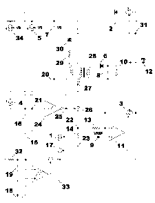
Figure 1 is a schematic diagram of the preferred embodiment of the present
invention.
Figure 2 is an illustration of voltage waveforms developed under operation at
junction points as referenced
in Figure 1 essential to the understanding of the present invention.
Figure 3 is another illustration of voltage waveforms developed under
operation at junction points as
referenced in Figure 1 essential to the understanding of the present
invention.
DETAILED DESCRIPTION OF THE PREFERRED EMBODIMENT
In order to better understand the embodiment of the present invention, a wide
supply range flyback
converter will be described with reference to FIGURE 1. One terminal of a
timing capacitor 16 is
connected to a voltage controlled current sink 4 as in FIGURE 1 forming
junction 21. Voltage controlled
current source with gated threshold 2 and feed forward current source 5 are
further connected to said
junction point. Switched current source I is additionally connected to this
junction. This junction also
forms the input of inverted Schmitt trigger 24. A waveform as in FIGURE 2B is
developed at junction
point 21. The other terminal of said timing capacitor 16 is connected to
common ground 15. Ground points
15, 18, 20 and 23 represent a common point and are only separated for the
purposes of this illustration.
The output of said inverted Schmitt trigger 24 is connected to the input
terminal of a switching
element 26, such as a MOSFET, and is additionally connected to the other
terminal of voltage controlled
current sink 4 forming junction point 25. A waveform as in FIGURE 2C is
developed at junction point 25.
The first output terminal of switching element 26 is connected to the dotted
terminal of the primary
winding of transformer 28 forming junction point 27 where a waveform as in
FIGURE 2D is developed. In
FIGURE 2D, VSPjKf, denotes the maximum voltage point across switching element
26 which will decay to
the reflected voltage value, VREFUICrED . Transformer 28 further comprises a
secondary winding and a bias
winding. The other terminal of said primary winding of transformer 28 is
connected to the positive terminal
of the converter's DC supply 7, a power source typically derived from
rectified and filtered AC mains, the
other terminal of said feed forward current source 5, a terminal of voltage
controlled current source 34, and
2
CA 02591521 2007-05-31
a terminal of startup resistor 32. The negative terminal of said DC supply 7
is connected to common ground
20.
The second output terminal of switching element 26 is connected to a terminal
of sensing resistor
14 and the a terminal of a current sample feed resistor 13 forming junction
point 22. A waveform as in
FIGURE 2A is developed at junction point 22. The remaining terminal of said
current sample feed resistor
13 is connected to the negative input of current sense comparator 11, a
terminal of voltage controlled
current source 3, and the remaining terminal of voltage controlled current
source 34. The remaining
terminal of sensing resistor 14 is connected to common ground 23. The positive
input of said current sense
comparator 11 forms voltage reference point 9.
A terminal of the secondary winding of transformer 28 is connected to a
terminal of output
capacitor 8 and a terminal of load 10 forming the negative output of the
converter. The dotted tenninal of
the secondary winding of transformer 28 is connected the anode of rectifier 6.
The cathode of said rectifier
6 is connected to the remaining terminals of output capacitor 8 and load 10
forming the positive output of
the converter.
The output of said current sense comparator 11 is connected to the input of
switching element 17,
typically a transistor. An output terminal of said switching element 17 is
connected to the remaining
terminal of switched current source 1. The other output terminal of switching
element 17 is connected to
the output terminal of a typical under-voltage lockout circuit with hysteresis
33, the other terminal of
voltage controlled current source 3, the other terminal of voltage controlled
current source with gated
threshold 2, and the cathode of bias rectifier 30 forming junction point 31.
The input terminal of said under-
voltage lockout circuit with hysteresis 33 is connected to the remaining
terminal of startup resistor 32 and a
terminal of storage capacitor 19. The remaining terminal of said storage
capacitor 19 and the ground
terminal of said under-voltage lockout circuit with hysteresis 33 are
connected to common ground 18.
Said voltage controlled current sources with gated threshold 2 and voltage
controlled current
source 3 are both controlled by the signal developed at feedback point 12.
Feed forward current source 5
and voltage controlled current source 34 are controlled by DC supply 7.
The anode of said bias rectifier 30 is connected to a terminal of bias
resistor 29. The other terminal
of bias resistor 29 is connected to the dotted terminal of the bias winding of
transformer 28. The other
3
CA 02591521 2007-05-31
terminal of the bias winding of transformer 28 is connected to common ground
20.
In order to better understand the present invention, typical operation will be
described with
reference to the waveforms developed as shown in FIGURES 2 and 3. For the
purposes of this
explanation, t = 0 will be defined as the moment when the voltage on timing
capacitor 16 crosses the
lower threshold, Vj , of inverted Schmitt trigger 24 thus turning switching
element 26 on, wherein the
control waveform at junction point 25, as shown in FIGURE 2C, is produced and
lasts for the duration of
the on time. Said on time is defined as the time required for the current to
ramp up to the current sense
threshold as demonstrated by the voltage waveform arising at junction point
22, as shown in FIGURE 2A,
which is proportional to the current through current sense resistor 14. The
proportionality factor is the
resistance of current sense resistor 14. The voltage appearing at junction 22
is combined at the negative
input of current sense comparator 11 with the feedback signal provided via
voltage controlled current
source 3 therein reducing the current sense threshold in response to a load
reduction and an increase in the
supply voltage sample. When this combination exceeds the value of the
reference at voltage reference point
9, the current sense comparator turns switching element 17 on, thereby
allowing switched current source 1
to rapidly charge timing capacitor 16 to above the upper threshold, VH , of
inverted Schmitt trigger 24. At
this point, the on time of switching element 26 will be terminated and timing
capacitor 16 will be
discharged by the sum of the currents of voltage controlled current sink 4,
voltage controlled current source
with gated threshold 2, and feed forward current source 5 until the voltage
reaches V, again thus initiating
a new cycle.
Since the discharge value of voltage controlled current sink 4 is reduced by
feed forward current
source 5, proportional to DC supply 7 voltage, Vti , power supply rejection is
greatly improved together
with the overload condition when high line voltage is applied. This is
achieved by increasing off time at a
rate faster than on time is decreased due to the current slope increase
through switching element 26 as per
V di
where V is the voltage at DC supply 7 and L is the magnetic inductance of the
primary
L dt
winding of said transformer 28. The net effect will be a drop in frequency
which in turn will decrease
switching losses at high line and conduction losses at low line.
4
CA 02591521 2007-05-31
Since the sensed peak current through the magnetizing winding of transformer
28 varies with
changes in supply voltage due to the turn off delay between junction 22 and
junction 25, thereby resulting
in increased sensed current error with increased supply voltage, voltage
controlled current source 34 is used
to compensate for this error. Thus, voltage controlled current source 34 can
be designed to keep the peak of
the sensed current relatively constant with respect to supply voltage
variation.
The signal at feedback point 12 initially modifies (reduces) current sense
threshold in response to
a load current decrease and thereby reduces the on time. When said feedback
signal reaches a
predetermined level, voltage controlled current source with gated threshold 2
will be activated as well and a
simultaneous on time reduction and off time increase will be achieved
resulting in high light load
efficiencies. Voltage controlled current source with gated threshold 2 is
typically set to be activated when
the signal at feedback point 12 exceeds the lower threshold, VL, of inverted
Schmitt trigger 24. The voltage
waveform at junction 21 across timing capacitor 16 is shown in FIGURE 2B and
the typical voltage
waveform at junction 27 is shown in FIGURE 2D.
Another important feature of the operation of the present invention is the
inherent noise filtration
of the current waveform. The typical current waveform appearing at junction 22
is not nearly as ideal as
that depicted in FIGURE 2A. FIGURE 3A shows the control waveform of switching
element 26 and the
non-ideal current response is shown in FIGURE 3B wherein the leading edge of
the current waveform
contains a spike 35 due to the input capacitance of switching element 26. This
current spike 35, which
easily reaches above the current sense threshold, Vn.s , would reset the
inverted Schmitt trigger 24 if this
was not counteracted by the integrating effect of timing capacitor 16 and
switched current source 1. The
actual effect of the spike 35 of the waveform at junction 21, the input of
inverted Schmitt trigger 24, is
shown in FIGURE 3C wherein a voltage increase of dV is not sufficient to trip
said inverted Schmitt
trigger 24 to the off condition. Therein, the integrator formed by timing
capacitor 16 and switched current
source I greatly reduces chances of false triggering. FIGURE 3C further shows
an off time discharge
pattern typical to the implementation of a resistor in place of voltage
controlled current sink 4.
Yet another feature of the operation of the present invention is related to
the overload condition.
Bias rectifier 30 can be chosen to have a limited but sufficiently large
reverse recovery time such that bias
rectifier 30 in conjunction with bias resistor 29 will be average responding.
Therefore, under overload
5
CA 02591521 2007-05-31
condition, the bias voltage at junction 31 can be made to collapse
sufficiently with the output voltage across
load 10 to disable the operation of the converter by means of typical under-
voltage lockout circuitry 33.
Yet another feature of the operation of the present invention is related to
the no load condition.
Therein, a low frequency load hunting operation of the under-voltage lockout
circuitry 33 will be invoked,
one cycle of which will be described herein. In order to achieve low power
consumption under no load
condition, the above mentioned rectification scheme of the bias voltage,
utilizing bias rectifier 30 and bias
resistor 29, is chosen such that at loads approaching 1% of the nominal full
load value, said bias voltage
average will be sufficiently small to trip the lockout feature of said under-
voltage lockout circuit with
hysteresis 33 whereby the converter is disabled for the duration required for
startup resistor 32 to charge
storage capacitor 19 to the positive going threshold, VH 7"40 , of under-
voltage lockout circuitry 33 lasting
several hundred milliseconds. When said positive going threshold has been
reached, the converter turns on
for a few milliseconds and in the absence of loads greater than 1% of the
nominal full load value, the
voltage on capacitor 19 will drop again below the level of the negative going
threshold, V~~xu) , of under-
voltage lockout circuitry 33 thereby initiating a new cycle.
Although the present invention has been described in relation to particular
embodiments thereof,
many other variations, modifications, and other uses will become apparent to
those skilled in the art.
Therefore, the present invention should be limited not by specific disclosures
herein, but only by the
appended claim.
6