Note: Descriptions are shown in the official language in which they were submitted.
CA 02591799 2007-07-09
MOBILE WIRELESS COMMUNICATIONS DEVICE HAVING DUAL ANTENNA
SYSTEM FOR CELLULAR AND WiFi
Field of the Invention
The present invention relates to the field of conununications devices, and
more
particularly, to communications devices that use dual antenna systems.
Background of the Invention
Cellular communication systems continue to grow in popularity and have become
an integral part of both personal and business communications. Cellular
telephones and
similar devices allow users to place and receive phone calls most anywhere
they travel.
Moreover, as cellular telephone technology is increased, so too has the
functionality of
cellular devices. For example, many cellular devices now incorporate Personal
Digital
Assistant (PDA) features such as calendars, address books, task lists,
calculators, memo
and writing programs, etc. These multi-function devices usually allow users to
send and
receive electronic mail (email) messages wirelessly and access the internet
via a cellular
network and/or a wireless local area network (WLAN), for example, when the
devices
include appropriate circuitry for WiFi and other IEEE 802.11 WLAN access.
Many of the cellular communications use packet burst transmissions as part of
a
Global System for Mobile communications (GSM) system, which includes the 850
MHz,
900 MHz, 1800 MHz and 1900 MHz frequency bands. Although these mobile wireless
communication devices function as a cellular telephone, as noted before, the
device can
also operate and incorporate Persotial Digital Assistant (PDA) features and
send and
receive email and other messages wirelessly and across the internet via the
cellular
network and/or a wireless Local Area Network (LAN). This function can include
access
to "hot spots" as part of a WiFi network using IEEE 802.11 standards.
When such devices incorporate WiFi technology, the circuits could be
considered
to describe WLAN products based on IEEE 802.11 standards, using one or more
Access
Points (APs) as "hot spots" and various numbers of clients. An AP typically
broadcasts a
Service Set Identifier, "network name" (SSID), using packets called "beacons"
by some
skilled in the art, which are broadcast every one hundred or so milliseconds
at about one
I
CA 02591799 2007-07-09
Mbit\s duration in some non-limiting examples. Some of these WiFi devices
operate in
the 2.4 or 5.0 GHz band.
A wireless access point usually connects wireless stations to an adjacent,
wired
local area network, and is operative similar to an Ethernet hub. The access
point can relay
wireless data to other compatible wireless devices and to a single, connected
local area
network device, such as a Ethernet hub or switch. Wireless routers are often
used to
integrate a wireless access point with a Ethernet switch and Ethernet router.
In a mobile wireless communications device, if the cellular capability is
integrated
with WiFi capability, often two different antennas are used, for example, a
main cellular
antenna operative at GSM or other CDMA band and a WiFi antenna operative in
the at
least 2.4 GHz band, and sometimes the 5.0 GHz band, making the device not only
compatible with cellular GSM communications, but also compatible with WiFi
communications using IEEE 802.11 standards. The antenna designs become more
challenging, however, as the size and thickness of the mobile phones become
smaller to
meet marketing requirements and the desires of end-use consumers. In order to
implement
multiple antennas in a compact environment, the antennas should be designed to
reduce
the coupling between the various antennas. This is necessary not only to
enhance radio
performance, but also reduce the cost of implementing Electromagnetic
Interference
(EMI) filters at harmonic frequencies. Thus, the type of antenna designs used
in such
devices become important to reduce the mutual coupling due to the third
harmonics
between a GSM or similar cellular antenna, operative, for example, at 850 MHz,
and a
WiFi antenna operative at 2.4 GHz. Isolatirig these antennas can be difficult,
and different
feeding techniques should be introduced to enhance isolation between the two
antennas.
The two systems, cellular as a Wide Area Network (WAN) and WiFi need to work
simultaneously, and thus, isolation between antennas is very critical.
Summary of the Invention
A mobile wireless communications device includes a housing and circuit board
carried by the housing. Radio Frequency (RF) circuitry is mounted on the
circuit board.
A first antenna is supported by the circuit board within the housing and
operatively
connected to the RF circuitry and configured for cellular phone
communications. A
2
CA 02591799 2007-07-09
second antenna is supported by the circuit board within the housing and
operatively
connected to the RF circuitry and configured for WiFi communications. The
second
antenna comprises an inverted-F or monopole antenna having an opening gap that
is
pointed away from the first antenna.
In yet another aspect, the first antenna is operative at frequencies in the
Global
System for Mobile (GSM) communications band (or CDMA). The second antenna is
operative at the 2.4 GHz and 5.0 GHz band in accordance with 802.11 standards.
The
second antenna can include a feeding point positioned distal from the opening
gap at an
opposing end from the opening gap. The housing can include an upper and lower
portion.
In one aspect the first antenna is positioned at a lower portion of the
housing and the
second antenna is mounted on the circuit board at an upper portion of the
housing. The
opening gap is positioned upward toward the upper portion of the housing in
one non-
limiting example.
In yet another aspect, the circuit board can be formed as a ground plane for
the first
and second antennas. The second antenna is substantially rectangular
configured in plan
view in one non-limiting exampleznd includes an upper edge that forms the
opening gap
of the inverted-F or monopole antenna. A lower edge fonns a lower leg of the
antenna.
This lower edge or leg could include a feeding point and grounding point at
opposite
corners thereof, which could be reversed from each other. In another non-
limiting
example, the second antenna can be configured at a quarter or half lamda in
length.
In accordance with one non-limiting example, the WiFi antenna is operative in
the
2.4 GHz frequency bands in this non-limiting example, and is bottom-fed
relative to the
cellular antenna, which is also positioned in the housing. This relative
positioning reduces
mutual coupling to the cellular, e.g., GSM 850 MHz antenna at its third
harmonic
frequency. For purposes of clarity and description, the term WiFi antenna can
refer to any
number of antennae that are operative in these frequency bands in accordance
with IEEE
802.11 and similar standards. Also included under this term WiFi antenna could
be
different Bluetooth applications.
The WiFi antenna could be a quarter or half lamda long and preferably is
formed
as an inverted-F or monopole type antenna. The opening gap in the inverted-F
or
monopole type antenna faces away from the cellular, e.g., GSM antenna (or
CDMA)
3
CA 02591799 2007-07-09
positioned preferably at the lower portion of the device housing. The inverted-
F or
monopole type WiFi antenna is positioned on the main Printed Circuit Board
(PCB) of the
wireless device, such as at an upper portion. This PCB also serves as a ground
plane for
the antennas. The WiFi antenna includes a feeding point and a grounding point,
positioned preferably at the lower portion of the inverted-F or monopole type
antenna,
opposite the opening gap. These two positions for the grounding point and
feeding point
could be interchangeable. It should also be understood that the inverted-F or
monopole
antenna could be used for other non-WiFi applications, such as GPS.
Brief Description of the Drawings
Other objects, features and advantages will become apparent from the detailed
description which follows when considered in light of the accompanying
drawings in
which:
FIG. 1 is a schematic block diagram of an example of a mobile wireless
communications device configured as a handheld device that can be used in
accordance
with non-limiting examples and illustrating basic internal components thereof.
FIG. 2 is a front elevation view of the mobile wireless communications device
of
FIG. 1.
FIG. 3 is a schematic block diagram showing basic functional circuit
components
that can be used in the mobile wireless communications device of FIGS. 1-2.
FIG. 4 is a plan view showing the interior of a mobile wireless communications
device similar to those shown in FIGS. I through 3 and showing in greater
detail the
relative positioning of a WiFi antenna and a cellular (or GSM) antenna.
FIG. 5 is a fragmentary, side elevation view of the communications device such
as
shown in FIG. 4 and showing a fragmentary representation of the circuit board
and the
configuration of a bottom-fed WiFi antenna formed as an inverted-F antenna,
and showing
an opening gap facing up and its position relative to the cellular antenna, in
accordance
with a non-limiting example.
FIG. 6 is a fragmentary, top plan view of the circuit board shown in FIG. 5,
and
showing the location of the cellular antenna, the location of WiFi antenna
formed as an
4
CA 02591799 2007-07-09
inverted-F antenna, and location of the grounding and feeding points at
opposite, lower
corners of the inverted-F antenna, in accordance with a non-limiting example.
Detailed Description of the Preferred Embodiments
Different embodiments will now be described more fully hereinafter with
reference
to the accompanying drawings, in which preferred embodiments are shown. Many
different forms can be set forth and described embodiments should not be
construed as
limited to the embodiments set forth herein. Rather, these embodiments are
provided so
that this disclosure will be thorough and complete, and will fully convey the
scope to those
skilled in the art. Like numbers refer to like elements throughout.
A brief description will now proceed relative to FIGS. 1-3, which disclose an
example of a mobile wireless communications device, for example, a handheld
portable
cellular radio, which can incorporate non-limiting examples of various
circuits that can be
used with the cellular antenna and WiFi antenna. FIGS. 1-3 are representative
non-
limiting examples of the many different types of functional circuit components
and their
interconnection, and operative for use with the antenna as later described
below.
Referring initially to FIGS. 1 and 2, an example of a mobile wireless
communications device 20, such as a handheld portable cellular radio is first
described.
This device 20 illustratively includes a housing 21 having an upper portion 46
and a lower
portion 47, and a dielectric substrate (i.e., circuit board) 67, such as a
conventional printed
circuit board (PCB) substrate, for example, carried by the housing. A housing
cover (not
shown in detail) would typically cover the front portion of the housing. The
term circuit
board 67 as used hereinafter can refer to any dielectric substrate, PCB,
ceramic substrate
or other circuit carrying structure for carrying signal circuits and
electronic components
within the mobile wireless communications device 20. The illustrated housing
21 is a
static housing, for example, as opposed to a flip or sliding housing, which is
used in many
cellular telephones. However, these and other housing configurations may also
be used.
Circuitry 48 is carried by the circuit board 67, such as a microprocessor,
memory,
one or more wireless transceivers (e.g., cellular, WLAN, etc.), which includes
RF
circuitry, including audio and power circuitry, including any keyboard
circuitry. It should
be understood that keyboard circuitry could be on a separate keyboard, etc.,
as will be
CA 02591799 2007-07-09
appreciated by those skilled in the art. A battery (not shown) is also
preferably carried by
the housing 21 for supplying power to the circuitry 48. The term RF circuitry
could
encompass the interoperable RF transceiver circuitry, power circuitry and
audio circuitry.
Furthermore, an audio output transducer 49 (e.g., a speaker) is carried by an
upper
portion 46 of the housing 21 and connected to the circuitry 48. One or more
user input
interface devices, such as a keypad (keyboard) 23 (FIG. 2), is also preferably
carried by
the housing 21 and connected to the circuitry 48. The term keypad as used
herein also
refers to the term keyboard, indicating the user input devices having lettered
and/or
numbered keys commonly known and other embodiments, including multi-top or
predictive entry modes. Other examples of user input interface devices include
a scroll
whee137 and a back button 36. Of course, it will be appreciated that other
user input
interface devices (e.g., a stylus or touch screen interface) may be used in
other
embodiments.
A cellular antenna 45, for example, a GSM antenna, is preferably positioned at
the
lower portion 47 in the housing and can be formed as a pattern of conductive
traces that
make an antenna circuit, which physically forms the antenna. This cellular
antenna is
connected to the circuitry 48 on the main circuit board 67. In one non-
limiting example,
the cellular antenna could be formed on an antenna circuit board section that
extends from
the main circuit board at the lower portion of the housing. An example of a
cellular
antenna that could be used or modified for use is disclosed in commonly
assigned U.S.
Patent Publication No. 2006/0172785. By placing the cellular antenna 45
adjacent the
lower portion 47 of the housing 21, the distance is advantageously increased
between the
cellular antenna and the user's head when the phone is in use to aid in
complying with
applicable SAR requirements. Also, a separate keyboard circuit board could be
used. The
WiFi antenna (not shown in this figure) can be located away from the cellular
antenna 45,
as explained in greater detail below.
More particularly, a user will typically hold the upper portion of the housing
21
very close to his head so that the audio output transducer 49 is directly next
to his ear.
Yet, the lower portion 47 of the housing 21 where an audio input transducer
(i.e.,
microphone) is located need not be placed directly next to a user's mouth, and
can be held
away from the user's mouth. That is, holding the audio input transducer close
to the user's
6
CA 02591799 2007-07-09
mouth may not only be uncomfortable for the user, but it may also distort the
user's voice
in some circumstances.
Another important benefit of placing the cellular antenna 45 adjacent the
lower
portion 47 of the housing 21 is that this may allow for less impact on antenna
performance
due to blockage by a user's hand. That is, users typically hold cellular
phones toward the
middle to upper portion of the phone housing, and are therefore more likely to
put their
hands over such an antenna than they are an antenna mounted adjacent the lower
portion
47 of the housing 21. Accordingly, more reliable performance may be achieved
by
placing the cellular antenna 45 adjacent the lower portion 47 of the housing
21.
Still another benefit of this configuration is that it provides more room for
one or
more auxiliary input/output (UO) devices 50 to be carried at the upper portion
46 of the
housing. Furthermore, by separating the cellular antenna 45 from the auxiliary
I/O
device(s) 50, this may allow for reduced interference therebetween.
Examples of auxiliary UO devices 50 include a WiFi or WLAN (e.g., Bluetooth,
IEEE 802.11) antenna for providing WLAN communication capabilities, as will be
explained in greater detail below, and/or a satellite positioning system
(e.g., GPS, Galileo,
etc.) antenna for providing position location capabilities, as will be
appreciated by those
skilled in the art. Other examples of auxiliary I/O devices 50 include a
second audio
output transducer (e.g., a speaker for speaker phone operation), and a camera
lens for
providing digital camera capabilities, an electrical device connector (e.g.,
USB,
headphone, secure digital (SD) or memory card, etc.).
It should be noted that the term "input/output" as used herein for the
auxiliary I/O
device(s) 50 means that such devices may have input and/or output
capabilities, and they
need not provide both in all embodiments. That is, devices such as camera
lenses may
only receive an optical input, for example, while a headphone jack may only
provide an
audio output.
The device 20 further illustratively includes a display 22, for example, a
liquid
crystal display (LCD) carried by the housing 21 and connected to the circuitry
48. A back
button 36 and scroll wheel 37 can also be connected to the circuitry 48 for
allowing a user
to navigate menus, text, etc., as will be appreciated by those skilled in the
art. The scroll
wheel 37 may also be referred to as a "thumb wheel" or a "track wheel" in some
instances.
7
CA 02591799 2007-07-09
The keypad 23 illustratively includes a plurality of multi-symbol keys 24 each
having
indicia of a plurality of respective symbols thereon. The keypad 23 also
illustratively
includes an alternate function key 25, a next key 26, a space key 27, a shift
key 28, a
return (or enter) key 29, and a backspace/delete key 30.
The next key 26 is also used to enter a"*" symbol upon first pressing or
actuating
the alternate function key 25. Similarly, the space key 27, shift key 28 and
backspace key
30 are used to enter a "0" and "#", respectively, upon first actuating the
alternate function
key 25. The keypad 23 further illustratively includes a send key 31, an end
key 32, and a
convenience (i.e., menu) key 39 for use in placing cellular telephone calls,
as will be
appreciated by those skilled in the art.
Moreover, the symbols on each key 24 are arranged in top and bottom rows. The
symbols in the bottom rows are entered when a user presses a key 24 without
first pressing
the alternate function key 25, while the top row symbols are entered by first
pressing the
alternate function key. As seen in FIG. 2, the multi-symbol keys 24 are
arranged in the
first three rows on the keypad 23 below the send and end keys 31, 32.
Furthermore, the
letter symbols on each of the keys 24 are arranged to define a QWERTY layout.
That is,
the letters on the keypad 23 are presented in a three-row format, with the
letters of each
row being in the same order and relative position as in a standard QWERTY
keypad.
Each row of keys (including the fourth row of function keys 25-29) is arranged
in
five columns. The multi-symbol keys 24 in the second, third, and fourth
columns of the
first, second, and third rows have numeric indicia thereon (i.e., 1 through 9)
accessible by
first actuating the alternate function key 25. Coupled with the next, space,
and shift keys
26, 27, 28, which respectively enter a"*", "0", and "#" upon first actuating
the alternate
function key 25, as noted above, this set of keys defines a standard telephone
keypad
layout, as would be found on a traditional touch-tone telephone, as will be
appreciated by
those skilled in the art.
Accordingly, the mobile wireless communications device 20 as described may
advantageously be used not only a's a traditional cellular phone, but it may
also be
conveniently used for sending and/or receiving data over a cellular or other
network, such
as Internet and email data, for example. Of course, other keypad
configurations may also
8
CA 02591799 2007-07-09
be used in other embodiments. Multi-tap or predictive entry modes may be used
for
typing e-mails, etc. as will be appreciated by those skilled in the art.
The cellular antenna 45 is preferably formed as a multi-frequency band
antenna,
which provides enhanced transmission and reception characteristics over
multiple
operating frequencies. More particularly, the cellular antenna 45 is designed
to provide
high gain, desired impedance matching, and meet applicable SAR requirements
over a
relatively wide bandwidth and multiple cellular frequency bands. By way of
example, the
cellular antenna 45 preferably operates over five bands, namely a 850 MHz
Global System
for Mobile Communications (GSM) band (GSM 850), a 900 MHz GSM band, a DCS
band, a PCS band, and a WCDMA band (i.e., up to about 2100 MHz) (or CDMA
850/1900), although it may be used for other bands/frequencies as well. To
conserve
space, the cellular antenna 45 may advantageously be implemented in three
dimensions
although it may be implemented in two-dimensional or planar embodiments as
well.
The mobile wireless communications device shown in FIGS. I and 2 can
incorporate e-mail and messaging accounts and provide different functions such
as
composing e-mail, PIN messages, and SMS messages. The device can manage
messages
through an appropriate menu that can be retrieved by choosing a messages icon.
An
address book function could add contacts, allow management of an address book,
set
address book options and manage SIM card phone books. A phone menu could allow
for
the making and answering of phone calls using different phone features,
managing phone
call logs, setting phone options, and viewing phone information. A browser
application
could permit the browsing of web pages, configuring a browser, adding
bookmarks, and
changing browser options. Other applications could include a task, memo pad,
calculator,
alarm and games, as well as handheld options with various references.
A calendar icon can be chosen for entering a calendar program that can be used
for
establishing and managing events such as meetings or appointments. The
calendar
program could be any type of messaging or appointment/meeting program that
allows an
organizer to establish an event, for example, an appointment or meeting.
A non-limiting example of various functional components that can be used
in the exemplary mobile wireless communications device 20 of FIGS. 1 and 2 is
further
described in the example below with reference to FIG. 3. The device 20
illustratively
9
CA 02591799 2007-07-09
includes a housing 120, a keypad 140 and an output device 160. The output
device 160
shown is preferably a display, which is preferably a full graphic LCD. Other
types of
output devices may alternatively be used. A processing device 180 is contained
within the
housing 120 and is coupled between the keypad 140 and the display 160. The
processing
device 180 controls the operation of the display 160, as well as the overall
operation of the
mobile device 20, in response to actuation of keys on the keypad 140 by the
user.
The housing 120 may be elongated vertically, or may take on other sizes and
shapes (including clamshell housing structures). The keypad may include a mode
selection
key, or other hardware or software for switching between text entry and
telephony entry.
In addition to the processing device 180, other parts of the mobile device 20
are
shown schematically in FIG. 3. These include a conununications subsystem 101;
a short-
range communications subsystem 102; the keypad 140 and the display 160, along
with
other input/output devices 106, 108, 110 and 112; as well as memory devices
116, 118 and
various other device subsystems 121. The mobile device 20 is preferably a two-
way RF
communications device having voice and data communications capabilities. In
addition,
the mobile device 20 preferably has the capability to communicate with other
computer
systems via the Internet.
Operating system software executed by the processing device 180 is preferably
stored in a persistent store, such as the flash memory 116, but may be stored
in other types
of memory devices, such as a read only memory (ROM) or similar storage
element. In
addition, system software, specific device applications, or parts thereof, may
be
temporarily loaded into a volatile store, such as the random access memory
(RAM) 118.
Communications signals received by the mobile device may also be stored in the
RAM
118.
The processing device 180, in addition to its operating system functions,
enables
execution of software applications 130A-130N on the device 20. A predetermined
set of
applications that control basic device operations, such as data and voice
communications
130A and 130B, may be installed on the device 20 during manufacture. In
addition, a
personal information manager (PIM) application may be installed during
manufacture.
The PIM is preferably capable of organizing and managing data items, such as e-
mail,
calendar events, voice mails, appointments, and task items. The PIM
application is also
CA 02591799 2007-07-09
preferably capable of sending and receiving data items via a wireless network
141.
Preferably, the PIM data items are seamlessly integrated, synchronized and
updated via
the wireless network 141 with the device user's corresponding data items
stored or
associated with a host computer system.
Communication functions, including data and voice communications, are
performed through the communications subsystem 101, and possibly through the
short-
range communications subsystem. The communications subsystem 101 includes a
receiver
150, a transmitter 152, and one or more antennae 154 and 156. In addition, the
communications subsystem 101 also includes a processing module, such as a
digital signal
processor (DSP) 158, and local oscillators (LOs) 161. The specific design and
implementation of the communications subsystem 101 is dependent upon the
communications network in which the mobile device 20 is intended to operate.
For
example, the mobile device 20 may include a communications subsystem 101
designed to
operate with the MobitexTM, Data TACTM or General Packet Radio Service (GPRS)
mobile data communications networks, and also designed to operate with any of
a variety
of voice communications networks, such as AMPS, TDMA, CDMA, PCS, GSM, etc.
Other types of data and voice networks, both separate and integrated, may also
be utilized
with the mobile device 20.
Network access requirements vary depending upon the type of communication
system. For example, in the Mobitex and DataTAC networks, mobile devices are
registered on the network using a unique personal identification number or PIN
associated
with each device. In GPRS networks, however, network access is associated with
a
subscriber or user of a device. A GPRS device therefore requires a subscriber
identity
module, commonly referred to as a SIM card, in order to operate on a GPRS
network.
When required network registration or activation procedures have been
completed,
the mobile device 20 may send and receive communications signals over the
communication network 141. Signals received from the communications network
141 by
the antenna 154 are routed to the receiver 150, which provides for signal
amplification,
frequency down conversion, filtering, channel selection, etc., and may also
provide analog
to digital conversion. Analog-to-digital conversion of the received signal
allows the DSP
158 to perform more complex communications functions, such as demodulation and
11
CA 02591799 2007-07-09
decoding. In a similar manner, signals to be transmitted to the network 141
are processed
(e.g., modulated and encoded) by the DSP 158 and are then provided to the
transmitter
152 for digital to analog conversion, frequency up conversion, filtering,
amplification and
transmission to the communication network 141 (or networks) via the antenna
156.
In addition to processing communications signals, the DSP 158 provides for
control of the receiver 150 and the transmitter 152. For example, gains
applied to
communications signals in the receiver 150 and transmitter 152 may be
adaptively
controlled through automatic gain control algorithms implemented in the DSP
158.
In a data communications mode, a received signal, such as a text message or
web
page download, is processed by the communications subsystem 101 and is input
to the
processing device 180. The received signal is then further processed by the
processing
device 180 for an output to the display 160, or alternatively to some other
auxiliary UO
device 106. A device user may also compose data items, such as e-mail
messages, using
the keypad 140 and/or some other auxiliary I/O device 106, such as a touchpad,
a rocker
switch, a thumb-wheel, or some other type of input device. The composed data
items may
then be transmitted over the communications network 141 via the communications
subsystem 101.
In a voice communications mode, overall operation of the device is
substantially
similar to the data communications mode, except that received signals are
output to a
speaker 110, and signals for transmission are generated by a microphone 112.
Alternative
voice or audio I/O subsystems, such as a voice message recording subsystem,
may also be
implemented on the device 20. In addition, the display 160 may also be
utilized in voice
communications mode, for example to display the identity of a calling party,
the duration
of a voice call, or other voice call related information.
Any short-range communications subsystem enables communication between the
mobile device 20 and other proximate systems or devices, which need not
necessarily be
similar devices. For example, the short-range communications subsystem may
include an
infrared device and associated circuits and components, or a BluetoothTM
communications
module to provide for communication with similarly-enabled systems and
devices.
It should be understood that GSM is one type of preferred communications
system
and uses a radio interface that can have an uplink frequency band and downlink
frequency
12
CA 02591799 2007-07-09
band with about 25 MHz bandwidth, typically subdivided into 124 carrier
frequency
channels, each spaced about 200 KHz apart as non-limiting examples. Time
division
multiplexing can be used to allow about 8 speech channels per radio frequency
channel,
giving 8 radio time slots and 8 burst periods grouped into what is called a
TDMA frame.
For example, a channel data rate could be about 270.833 Kbps and a frame
duration of
about 4.615 milliseconds (MS) in one non-limiting example. The power output
can vary
from about I to about 2 watts.
Linear predictive coding (LPC) can also be used to reduce the bit rate and
provide
parameters for a filter to mimic a vocal track with speech encoded at about 13
Kbps. Four
different cell sizes can be used in a GSM network, including macro, micro,
pico and
umbrella cells. A base station antenna can be installed on a master building
above the
average rooftop level in a macrocell. In a microcell, the antenna height can
be under the
average rooftop level and used in urban areas. Microcells typically have a
diameter of
about a few dozen meters and are used indoors. Umbrella cells can cover
shadowed
regions or smaller cells. Typically, the longest distance for the GSM
specification covered
by an antenna is about 22 miles depending on antenna height, gain and
propagation
conditions.
GSM systems typically include a base station subsystem, a network and
switching
subsystem, and a General Packet Radio Service (GPRS) core network. A
subscriber
identify module (SIM) is usually implemented in the communications device, for
example,
the well known SIM card, similar to a smart card containing the subscription
information
and phone book of a user. The user can also switch handsets or could change
operators by
changing a SIM.
The GSM signaling protocol has three general layers. Layer 1 is a physical
layer
using channel structures above the air interface. Layer 2 is the data link
layer. Layer 3 is
a signaling protocol, which includes three sublayers. These include a Radio
Resources
Management sublayer to control the setup, maintenance and terrnination of
radio and fixed
channels, including handovers. A Mobility Management sublayer manages the
location
updating and registration procedures and secures the authentication. A
Connection
Management sublayer handles general call control and manages supplementary
services
and the short message service. Signaling between different entities such as
the Home
13
CA 02591799 2007-07-09
Location Register (HLR) and Visiting Location Register (VLR) can be
accomplished
through a Mobile Application Part (MAP) built upon the Transaction
Capabilities
Application Part (TCAP) of the top layer of the Signaling System No. 7.
A Radio Resources Management (RRM) sublayer can oversee the radio and fixed
link establishment between the mobile station and an MSE.
It is also possible to used Enhanced Data Rates for GSM Evolution (EDGE), as
an
enhancement to General Packet Radio Service (GPRS) networks. EDGE can use 8
Phase
Shift Keying (8 PSK) and Gaussian Minimum Shift Keying (GMSK) for different
modulation and coding schemes. A three-bit word can be produced for every
changing
carrier phase. A rate adaptation algorithm can adapt the Modulation and Coding
Scheme
(MCS) according to the quality of the radio channel and the bit rate and
robustness of data
transmission. Base stations are typically modified for EDGE use.
FIG. 4 is a top plan view showing the interior of a mobile wireless
communications
device 200, such as described in FIGS. 1-3, but that incorporates the first
and second
antenna designs described above. Reference numerals begin in the 200 series
for the
description relative to FIGS. 4-6. The device 200 shown in FIG. 4 includes a
printed
circuit board 202 and various transducers 204 having a function as described
before. The
main cellular antenna 206 is illustrated at the bottom portion of the housing
208 and
corresponds to the antenna described before, and operative as a multi-
frequency antenna as
described before. The WiFi antenna 210 is positioned at the upper right corner
inside the
housing in this non-limiting example and shown as a rectangular configured
antenna. It is
operative at the 2.4 GHz frequency band in accordance with a non-limiting
example for
WiFi, WLAN and similar applications. It could be used for other applications
in some
non-limiting examples. A battery 212 and other electronic components 214 are
shown
positioned on the circuit board 202 as illustrated. This antenna 210 has its
feeding point
210a at the bottom edge or formed "leg" 210b and toward the cellular antenna
206 as
illustrated.
FIG. 5 is a fragmentary, side-elevation view showing the printed circuit board
202
that is operative as a ground plane. The WiFi antenna 210 is preferably formed
as an
inverted-F antenna and is bottom fed. This WiFi antenna 210 is positioned away
from the
cellular antenna 206 formed as a GSM antenna (or CDMA) in this non-limiting
example.
14
CA 02591799 2007-07-09
The cellular antenna 206 is positioned at the lower portion of the device
housing, and can
be configured as described before. The WiFi antenna 210 is positioned toward
the upper
portion of the housing and is bottom fed, such that the lower horizontal leg
210b that
forms part of the inverted-F is positioned towards the cellular antenna 206.
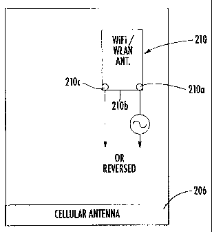
FIG. 6 is a plan view showing the feeding point 210a and a grounding point
210c
positioned at lower corners on the "leg" 210b relative to the cellular antenna
206, as
illustrated. The opening gap 210d formed by the inverted-F or monopole design
is
positioned opposite from the cellular antenna 206, towards the top or upper
portion of the
device as illustrated.
It should be understood that the design of the inverted-F or monopole antenna
210
can vary depending on end-use requirements and the nature of the housing,
circuit board,
proximity to the main cellular antenna, and other factors that could be
determined by those
skilled in the art. Typically, the height of the inverted-F is established by
the leg 210b
relative to the ground plane defined by the PCB 202. Input impedance at the
feeding point
210a can vary from about 30 to about 75 ohms, but centered at 50 ohms, in some
non-
limiting examples. Resonances can vary depending on the type of feeding lines
or traces
that are used.
The inverted-F antenna typically is a small size and is designed for ease of
design
and fabrication. This WiFI antenna 210 as described could be fed by a
microstrip line
printed on the printed circuit board 202. In some cases, the inverted-F
antenna could be
formed as an Active Inverted-F Antenna (AIFA) and printed on the PCB 202, for
example,
with a thickness of about 1 mm in one non-limiting example. Some designs could
use a
straight-F design and still be printed on a FR-4 or similar substrate with
other circuit
components to provide a low-cost antenna. For example, in a straight-F
antenna, an
inductive tuning arm could be on the same side of a capacitive arm. In any
event, the
antenna designs should be designed such that the opening gap 210d is
positioned to face
away from the cellular antenna 206, in these non-limiting examples.
In some non-limiting examples, an inverted-F antenna is similar to a free-
standing
(quarter-wave) monopole positioned above a ground plane, rather than a half-
wave printed
antenna in some non-limiting examples. The antenna can be formed in an area
less than
about 10 mm by 10 mm in non-liniiting examples. The inductive and capacitive
arms of
CA 02591799 2007-07-09
an inverted-F antenna could add to the total antenna length in some designs.
In other
antenna designs, it is possible to have a ground plane edge to determine
functional
characteristics and the operation band. An upper part of the "F" could be used
for
inductive tuning and a lower part of the "F" could be used to form a
capacitively coupled
monopole.
It is possible to apply Method of Moments (MoM) design considerations to wire
antennas of arbitrary shape to form a Dual Inverted-F Antenna (DIFA). It
should be
understood that the inverted-F antenna is a variation on a transmission line
antenna or bent
monopole antenna. It could include an offset feed to provide for adjustment of
the input
impedance in some non-limiting examples. Thus, the resulting antenna geometry
resembles the letter F, rotated to face the ground plane.
Many modifications and other embodiments of the invention will come to the
mind
of one skilled in the art having the benefit of the teachings presented in the
foregoing
descriptions and the associated drawings. Therefore, it is understood that the
invention is
not to be limited to the specific embodiments disclosed, and that
modifications and
embodiments are intended to be included within the scope of the appended
claims.
16