Note: Descriptions are shown in the official language in which they were submitted.
CA 02593093 2007-06-28
WO 2006/069450 PCT/CA2005/001987
COUPLING METHODS AND ARCHITECTURES FOR INFORMATION
PROCESSING
CROSS REFERENCE TO RELATED APPLICATIONS
This application claims priority to United States Patent Application No.
60/640,420, filed December 30, 2004 and United States Patent Application No.
11/247,857, filed October 10, 2005, each ofwhich is hereby incorporated herein
by
reference in its entirety.
1. FIELD OF THE INVENTION
This invention relates to the field of quantum computing and to the field of
superconducting devices.
2. SACKGROUND
In 1982, Richard Feynman proposed that a controllable quantum system could
be used to simulate other quantum systems more efficiently than conventional
computers. See Feymnan, 1982, International Journal of Theoretical Physics 21,
pp.
467-488, which is hereby incorporated by reference in its entirety. This
controllable
quantum system is now commonly referred to as a quantum computer, and effort
has
been put into developing a general purpose quantum computer that can be used
to
siinulate quantwn systems or run specialized quantum algorithms. In
particular,
solving a model for the behavior of a quantum system commonly involves solving
a
differential equation related to the Hamiltonian of the quantum system. David
Deutsch observed that a quantuni system could be used to yield a time savings,
later
shown to be an exponential time savings, in certain computations. If one had a
problem, modeled in the form of an equation that represented the Hamiltonian
of the
quantum system, the behavior of the system could provide information
regardiiig the
solutions to the equation. See Deutsch, 1985, Proceedings of the Royal Society
of
London A 400, pp. 97-117, which is hereby incorporated by reference in its
entirety.
One limitation in the quantun computing art is the identification of systems
that
can support quantum computation. The basis for performing quantum computation
is a
unit, which is hereinafter termed an information device. Infoimation devices
can have
many embodiments but must fulfill several requirements. One requireinent is
that the
information device must be reducible to a quanttun two-level system, which
meails that it
1
CA 02593093 2007-06-28
WO 2006/069450 PCT/CA2005/001987
must be able to have two distinguishable quantuin states that can be used for
computation.
The information devices must also be capable of producing quantum effects like
entanglement and superposition, described below. In general, the quantum
information
stored in an information devices can, but does not need to be, coherent. A
device with
coherency has a quantum state that persists without significant degradation
for a long
period of time, on the order of microseconds or more. One non-limiting example
of an
information device is a qubit, also termed a quantum bit. A qubit is analogous
to a bit in a
classical (digital) computer, and is a type of information device that
requires coherence.
The loss of coherence is referred to herein as decoherence.
The computing power of a quantum computer increases as its basic building
blocks, information devices, are coupled together in a controllable manner
such that
the quantuin state of one information device affects the quantum state of each
of the
information devices to which it is coupled. This form of coupling is referred
to as
entanglement. Another limitation in the quantuin computing art is the
identification
of methods that can be used to controllably entangle the states of information
devices
without introducing a significant source of decoherence.
2.1 Approaches to Quantum Computing
There are several general approaches to the design and operation of a quantum
computer. One approach that has been put forth is circuit model quantum
computing.
Circuit model quantum computing requires long quantum coherence, so the type
of
information device used in quantum computers that support such an approach are
qubits, which by definition should ideally have long coherence times. Circuit
model
quantum computing is based upon the premise that qubits can be acted on by
logical.
gates, much like bits, and can be programmed using quantum logic in order to
perform calculations. Research has been done to develop qubits that can be
programmed to perform quantum logic functions. For example, see Shor, 2001,
arXiv.org:quant-ph/0005003, which is hereby incorporated by reference in its
entirety.
However, reducing the decoherence of qubits such that many calculations can be
perforined before information stored in the qubit is destroyed has not been
successfully achieved in the art.
Another approach to quantum computing, called optimization quantum
conlputing, involves the use of a system of information devices to simulate a
quantum
system, This approach does not make critical use of quantum gates and
circuits.
2
CA 02593093 2007-06-28
WO 2006/069450 PCT/CA2005/001987
Instead, it relies upon quantum effects to manipulate the states of a system
of
interacting information devices starting from a known initial Hamiltonian so
that the
final state represents the Hamiltonian of the physical system in question. In
this
process, quantum coherence is not a requirement, so general information
devices, and
not just qubits, can be used as the computational building blocks. Examples of
this
type of approach are adiabatic quantum computing and simulated annealing,
which
are described in Farhi et al., 2002, arXiv.org:quant-ph/0201031, which is
hereby
incorporated by reference in its entirety.
2.2 Qubits
As mentioned previously, one possible information device is a qubit, also
known as a quantum bit. A qubit, wliile analogous to a digital bit in
classical
computers, has far more computational potential than a digital bit. Instead of
only
encoding one of two discrete states, like "0" and "1" as found in a digital
bit, a qubit
can also be placed in a superposition of "0 " and "1." That is, the qubit can
exist in
both the "0" and "1" state at the same time, and so can perform a quantum
coinputation on both states siinultaneously. In general, N qubits can be in a
superposition of 2N states. Quantum algoritluns make use of the superposition
property to speed up certain computations.
In standard notation, the basis states of a qubit are referred to as the 10)
and 11)
states. During quantum computation, the state of a qubit, in general, is a
superposition of
basis states so that the qubit has a nonzero probability of occupying the 10)
basis state and a
simultaneous nonzero probability of occupying the 11) basis state.
Mathematically, a
superposition of basis states means that the overall state of the qubit, which
is denoted IlI'),
has the form I LI') = aI 0) + bI1) , where a and b are coefficients
corresponding to the
probabilities Ja12 and Jb12, respectively. The coefficients a and b each have
real and
imaginary components, which allows the phase of the qubit to be characterized.
The
quantum nature of a qubit is largely derived from its ability to exist in a
coherent
superposition of basis states, and for the state of the qubit to have a phase.
A qubit will
retain this ability to exist as a coherent superposition of basis states when
the qubit is
sufficiently isolated from sources of decoherence.
To complete a computation using a qubit, the state of the qubit is measured
(e.g.,
read out). Typically, when a measurement of the qubit is done, the quantum
nature of the
3
CA 02593093 2007-06-28
WO 2006/069450 PCT/CA2005/001987
qubit is temporarily lost and the superposition of basis states collapses to
either the 10)
basis state or the 11) basis state, thus regaining its similarity to a
conventional bit. The
actual state of the qubit after it has collapsed depends on the probabilities
jaiz and lbl 2
immediately prior to the readout operation.
Information devices can have all the physical properties described above for
qubits. That is, the quantum state of an information device can be a
superposition of basis
states, and can be described by the forin I tI') = al 0) + bl 1) , where a and
b are coefficients
corresponding to the probabilities Ja12 and Jb12, respectively. The quantum
state of an
information device also collapses to a basis state when measured. However, as
mentioned
in Section 2.1, information devices no not have a stringent requirement for
quantum
coherence, as opposed to qubits.
2.3 Superconducting Information Devices
There are many different technologies that can be used to construct quantum
computers. One implementation uses superconducting materials. Quantum
computers constructed with superconducting information devices have the
advantage
of scalability. The possibility of realizing large scale quantum computers
using
superconducting information devices shows promise since the technologies and
processes involved in fabricating superconducting information devices are
similar to
those used for conventional computers, for which there already exists an
established
infrastructure of fabrication equipment and technological know-how. Such known
fabrication techniques (e.g., chemical vapor deposition, plasma enhanced
chemical
vapor deposition, etc.) are described, for example, in Van Zant, 2000,
Microchip
Fabrication, Fourth Edition, McGraw-Hill, New York; Levinson, 2001, Principles
of
Lithography, The International Society for Optical Engineering, Bellingham
Washington; Madou, 2002, Fundamentals ofMicrofabrication, Second Edition, CRC
Press LLC, Boca Raton, Florida; and Choudhury, 1997, Handbook of
Microlithography, Micromachining and Microfabrication Volume 1:
Microlithography, The International Society for Optical Engineering,
Bellingham
Washington, each of which is hereby incorporated by reference in its entirety.
Toward the realization of such a computer, Shnirman et al., 1997, Physics
Review
Letters 79, 2371-2374, which is hereby incorporated by reference in its
entirety,
proposed an embodiment of a superconducting quantum computer using
4
CA 02593093 2007-06-28
WO 2006/069450 PCT/CA2005/001987
superconducting information devices comprising Josephson junctions in order to
produce the required quantum effects.
Superconducting iizformation devices can be separated into several categories
depending on the physical property used to encode information. A general
division of
information devices separates them into charge and phase devices, as discussed
in
relation to qubits in Makhlin et al., 2001, Reviews of Modef=n Physics 73, pp.
357-
401, which is hereby incorporated by reference in its entirety. Charge devices
store
and manipulate information in the charge states of the device, where
elementary
charges consist of pairs of electrons called Cooper pairs. A Cooper pair has a
charge
of 2e and consists of two electrons bound together by a phonon interaction.
See, for
example, Nielson and Chuang, 2000, Quantum Computation and Quantum
Information, Cambridge University Press, Cambridge, pp. 343-345, which is
hereby
incorporated by reference in its entirety. Phase, or flux, devices, on the
other hand,
store information in the phase or flux states of the device. More recently,
hybrid
devices have been developed that can use both the charge and phase degrees of
freedom to control information. Some examples of hybrid devices are described
in
U.S. Patent No. 6,838,694 B2 to Esteve et al. as well as U.S. patent
application No.
10/934,049 to Amin et al., each of which is hereby incorporated by reference
in its
entirety.
2.4 Superconducting Flux Devices
Superconducting flux device designs are described in Bocko et al., 1997, IEEE
Transactions on Applied Superconductivity 7, p. 3638, as well as Makhlin et
al., 2001,
Review of Modern Physics 73, p. 357, each of which is hereby incorporated by
reference in its entirety. Many other superconducting flux device designs have
been
described, including the persistent current qubit. See Mooij et al., 1999,
Science 285,
1036; and Orlando et al., 1999, Physics Review B 60, 15398, which are hereby
incorporated by reference in their entireties. The persistent current qubit
consists of a
loop of thick superconducting material interrupted by tliree Josephson
junctions. The
critical current value of one Josephson junction is designed to be less than
that of the
other two Josephson junctions, which often have the same or very similar
critical
currents. The persistent current qubit can be built such that the loop of
5
CA 02593093 2007-06-28
WO 2006/069450 PCT/CA2005/001987
superconducting material encompasses a small area (e.g., an approximate area
of 1
micrometer squared).
The persistent current qubit has coherence times of between 10 nanoseconds
(ns) to 100 ns. See, for example, Orlando et al., 1999, Physics Review B 60,
15398,
and Il'ichev et al., 2003, Physics Review Letters 91, 097906, each of which is
hereby
incorporated by reference in its entirety. Some other types of flux devices
comprise
superconducting loops interrupt by either more or less than three Josephson
junctions.
See, e.g., Blatter et al., 2001, Physics Review B 63, 174511; and Friedman et
al.,
2000, Nature 406, 43, wluch are hereby incorporafied by reference in their
entireties.
Gradiometric flux devices are a special type of flux devices that are
insensitive
to homogenous magnetic fields. That is, a magnetic field which is homogenous
over
the entirety of a gradiometric flux device will not affect the quantum state
of the
device. An example of a gradiometric device is described in U.S. Patent No.
4,937,525 to Daalmans, which is hereby incorporated by reference in its
entirety.
Gradiometric flux device are discussed in more detail below.
2.5 Information Device Coupling
Regardless of which type of information device is used to construct a quantum
computer, it is desirable that the information devices of the quantum computer
interact with each other in a controllable manner. Such interaction between
the
informationdevices of a quantum computer is referred to as coupling. Depending
on
inipleinentation, different coupling methods can be used. Furthermore, a
system
Hamiltonian can be used to describe the states of the information devices of a
quantum computer as well as the interactions between the information devices.
In coupling two flux-based superconducting information devices together, the
sign of the coupling interaction in the system Hamiltonian determines the
energy
landscape of the system comprising the two devices. Generally, the coupling
between
two flux-based superconducting information devices is either ferromagnetic or
anti-
ferroinagnetic because flux devices typically interact via their respective
magnetic
fluxes. That is, a change in flux in one information device will affect the
flux of
another information device that is coupled to it. In ferromagnetic coupling,
it is
energetically favorable for a change in flux of a first information device to
produce a
similar change in the flux of a second information device that is coupled to
the first
information device. For example, an increase in flux in the first information
device
6
CA 02593093 2007-06-28
WO 2006/069450 PCT/CA2005/001987
will cause an increase in flux in the second information device when they are
ferromagnetically coupled. In the anti-ferromagnetic case, the coupling will
cause the
opposite effect on the coupled device (e.g. a flux increase in the first
device leads to a
flux decrease in the second coupled device) because it is more energetically
favorable.
By energetically favorable, it is meant that the quantum system prefers to be
in a
specific configuration because the energy is lower in the specific
configuration than in
other configurations.
. A flexible coupling scheme provides the ability to vary the strength of the
coupling between information devices, shut off coupling between such devices
altogether, andlor switch the sign of the coupling between such devices. By
switching
the sign of the coupling, it is meant that the type of coupling between two
information
devices is switched from ferromagnetic to anti-ferromagnetic or vice versa.
Switching the sign of the coupling in circuit model quantum computing is
useful for
constructing specific logic gates, such as the CNOT gate described in Plourde
et al.,
2004, arXiv.org:quant-ph/0406049, which is hereby incorporated by reference in
its
entirety. Switching the coupling sign in optimization quantum computing gives
greater flexibility to mapping problems that are to be solved by a quantum
computer
onto the quantum computer's information device grid. Here, the term
information
device grid refers to a set of information devices in a quantum computer in
which
each information device in the set is controllably coupled to at least one
other
information device in the set.
In one representation of the Hamiltonian of two flux information devices
coupled together, 6 67represents the "sigma z" coupling between two devices
with
a variable J as a pre-factor to indicate the strength of the coupling. When J>
0, the
coupling is anti-ferromagnetic, with a higher J meaning a stronger anti-
ferromagnetic
coupling. When J < 0, the coupling is ferromagnetic, with a lower J meaning a
stronger ferromagnetic coupling. When J = 0, there is no coupling. Thus,
switching
the sign of J switches the type of coupling. In the general case of a two-
level system,
ferromagnetic coupling implies it is energetically favorable to have parallel
fluxes and
anti-ferromagnetic coupling implies it is energetically favorable to have anti-
parallel
fluxes. An example of ferromagnetic and anti-ferromagnetic coupling is
coupling
between two flux devices with circulating currents in their respective loops.
7
CA 02593093 2007-06-28
WO 2006/069450 PCT/CA2005/001987
In ferromagnetic coupling, a clockwise superconducting current in a first
information device will cause a clockwise superconducting current to be more
energetically favorable than a counter-clockwise superconducting current in a
second
information device that is ferromagnetically coupled to the first device.
Conversely,
in ferromagnetic coupling, a counterclockwise superconducting current in the
first
device will cause a counterclockwise superconducting current to be more
energetically favorable than a clockwise superconducting current in the second
device. On the other hand, in anti-ferromagnetic coupling, a clockwise
superconducting current in the first infonnation device will make a
counterclockwise
superconducting current more energetically favorable than a clockwise
superconducting current in the second anti-ferromagnetically coupled device.
Further, in anti-ferromagnetic coupling, a counterclockwise superconducting
current
in the first device will make a clockwise superconducting current more
energetically
favorable than a counterclockwise superconducting current in the second
device.
Superconducting information devices can be inductively coupled in a direct
manner (e.g., without any intervening device), but this type of coupling is
typically
not controllable, meaning that the strength of the coupling cannot readily be
altered.
One way of coupling flux devices is through a superconducting quantum
interference
device, or SQUID.
A SQUID is a type of sensitive magnetometer, which means it can detect
small changes in magnetic flux. See, for example, U.S. Patent No. 6,627,916 to
Amin
et al., which is hereby incorporated by reference in its entirety. A SQUID
comprises
a superconducting loop interrupted by at least one Josephson junction. The
current
flowing in the superconducting loop of the SQUID can be biased in any of
several
different manners. For example, the current can be biased by an inductive flux
positioned close to the SQUID. In another the current can be biased using a
current
bias from a wire connected to the SQUID. Two examples of SQUIDs that differ in
the way they are biased are dc-SQUIDs (current or flux biased) and rf-SQUIDs
(flux
biased). SQUIDs can also generate flux in a controllable manner. Since flux
devices
interact via their magnetic fluxes, a SQUID-type device can be used to mediate
the
coupling, like the scheme suggested in Majer et al., 2003, arXiv.org:cond-
mat/0308192, which is hereby incorporated by reference in its entirety.
Mooij et al., 1999, Science 285, 1036, which is hereby incorporated by
reference in its entirety, propose a type of coupling scheme capable of
switching the
8
CA 02593093 2007-06-28
WO 2006/069450 PCT/CA2005/001987
type of coupling between two flux devices. However, Mooij has the drawback
that it
is not the ferromagnetic and anti-ferromagnetic coupling types that are
switched.
Rather, a switch between aZ aZ and 6 D 6x coupling is accomplished.
Further,
there is no way to completely turn off the couplirig in Mooij.
The inductive SQUID, or INSQUID, has been proposed as another coupling
device in Clarke et al., 2002, Physica Scripta T102, 173, which is hereby
incorporated
by reference in its entirety. INSQUID coupling can switch the type of
coupling, but
again it is not between ferromagnetic and anti-ferromagnetic coupling. It is
possible
to turn the INSQUID coupling off, but this is difficult to achieve.
A tunable flux transformer is described in Filippov et al., 2003, IEEE
Transactions on Applied Superconductivity 13, 1005, which is hereby
incorporated by
reference in its entirety. The tunable flux transfornler of Filippov et al.
relies on the
gradiometric nature of the employed device. The transformer itself is also
gradioinetric, and tunability is achieved by incorporating compound junctions
with
variable couplings. Thus, the transformer can be biased to couple or uncouple
a flux
device to a magnetometer or another device. However, the large gain that is
needed
creates the problem of imprecise balancing of the gradiometric loops of the
transformer. This leads to inaccuracy in maintaining a specified coupling
strength.
Also, the transformer is rather large (150 m x 150 m) and thus infeasible in
systems with a large number of devices. Lastly, the transformer is bistable,
or has two
energy minima, which is not preferred for coupling flux devices together.
Another type of gradiometric flux transformer was considered in Cosmelli et
al., 2004, arXiv.org:cond-mat/0403690, which is hereby incorporated by
reference in
its entirety. In Cosmelli et al., each arm of the gradiometer couples to one
adjacent
device, and the tunable element is a single compound junction in the central
leg. Yet
another rf-SQUID coupler is described in Plourde et al., 2004, Physical Review
B 70,
140501, which is hereby incorporated by reference in its entirety. In Plourde
et al.,
the coupling is mediated through a current biased dc-SQUID. The dc-SQUID can
be
tuned to switch the sign of the coupling. However, such systems are expensive
to
fabricate and cannot provide full flexibility in adjusting the strength or
sign of the
coupling.
Coupling flux devices together using a Josephson junction galvanically
connected to both flux devices has been proposed in Levitov et al., 2001,
9
CA 02593093 2007-06-28
WO 2006/069450 PCT/CA2005/001987
arXiv.org:cond-mat/0108266; and Butcher, 2002, Graduate Thesis, Delft
University
of Technology, each of which is hereby incorporated by reference in its
entirety. Both
references show a single large Josephson junction coupling a chain of three
Josephson
junction flux devices together. However, neither reference properly enables
the
operation of the coupling. Also, the type of coupling suggested in these
references is
always "on" and cannot be shut off.
2.6 State of the Art
As the above description indicates, there exist devices for coupling
superconducting information devices together. However, improvement in the
field is
desired in order to realize cost effective quantum computing. Thus, there
exists a
need in the art to provide more control over the coupling between
superconducting
information devices. What is desired is coupling that would allow for the
freedom to
change the strength or sign of the coupling between superconducting
information
devices as well as the ability to altogether shut the coupling off when
desired.
3. BRIEF DESCRIPTION OF TI3E DRAWINGS
Figure lA illustrates two information devices in a dual coupling scheme in
accordance with aii embodiment of the invention.
Figures 1B and 1C illustrate coupling devices or coupling elements in
accordance
with embodiments of the present invention.
Figure 2 illustrates two information devices in a dual coupling scheme in
accordance with another embodiment of the present invention.
Figure 3 illustrates a two-dimensional array of information devices that are
coupled to each other using a dual coupling scheme in accordance with an
embodiment of
the present invention.
Figure 4 illustrates a two-dimensional array of information devices that are
coupled to each other using a dual coupling scheme in accordance with another
embodiment of the present invention.
CA 02593093 2007-06-28
WO 2006/069450 PCT/CA2005/001987
Figure 5 illustrates a tunable coupling between flux devices using an rf-SQUID
in
accordance with an embodiment of the present invention.
Figure 6 is a graph of the total flux of an rf-SQUID versus the applied
external flux
in accordance with an embodiment of the present invention.
Figure 7 illustrates another tunable coupling between flux devices using a dc-
SQUID in accordance with an embodiment of the present invention.
Figure 8 is a graph of the normalized external current bias versus the
external flux
bias for a dc-SQUID in accordance with an embodiment of the present invention.
Figure 9 illustrates a tunable coupling between information devices using
direct
Josephson junction coupling in accordance with an embodiment of the present
invention.
Figure 10 illustrates another ttmable coupling between information devices
using
direct Josephson junction coupling in accordance with an embodiment of the
present
invention.
Figure 11 illustrates a fabrication metliod in accordance with an embodiment
of the
present invention.
Like reference numerals refer to corresponding parts throughout the several
views of the drawings.
4. SUMMARY OF THE INVENTION
One aspect of the present invention provides a structure comprising a first
and
a second flux device as well as a first and a second coupling element. The
first flux
device has at least a first lobe and a second lobe that are in electrical
communication
with each other. The second flux device has at least a first lobe and a second
lobe that
are in electrical communication with each other. The first coupling element
inductively couples the first lobe of the first flux device to the first lobe
of the second
flux device. The second coupling element inductively couples the first lobe of
the
11
CA 02593093 2007-06-28
WO 2006/069450 PCT/CA2005/001987
first flux device to the second lobe of the second flux device. The first and
second
coupling elements are not in electrical communication with each other. The
first and
second coupling element each have a dimensionless inductance that is between
0.5
and 2. In some embodiments, the first flux device and the second flux device
are
gradiometric flux devices.
In some embodiments, the at least first and second lobes of the first flux
device and the at least first and second lobes of the second flux device each
hold a
different circulating current configuration. In some embodiments, the first
coupling
element or the second coupling element couples the first flux device to the
second
flux device ferromagnetically or anti-ferromagnetically. In one embodiment,
the first
coupling element has no coupling strength and the second coupling element has
a
finite coupling strength.
In some embodiments, the structure further comprises a switch dimensioned
and configured relative to the first and second flux devices such that the
switch can
create a state in which both the first and second coupling elements have no
coupling
strength. In some embodiments, the structure further comprises a switch
dimensioned
and configured relative to the first and second flux devices such that the
switch can
toggle between a first state in which both the first and second coupling
elements have
a finite coupling strength and a second state in which both the first and
second
coupling elements have no coupling strength.
In some embodiments, the first coupling element, the second coupling
element, or both the first coupling element and the second coupling element
comprise
a dc-SQUID. In some embodiments, the first coupling element, the second
coupling
element, or both the first coupling and second coupling elements comprise an
rf-
SQUID. In some embodiments, the structure further comprises means for
controllably tuning the first coupling element, the second coupling element,
or both
the first and second coupling elements. In some embodiments, this switch
comprises
means for tuning the first and second coupling elements so that the first and
second
flux devices are not inductively coupled to each other. In some embodiments,
the first
and second flux devices are superconducting. In some embodiments, the
dimensionless inductance of the first and second coupling elements is between
0.5
and 1.5. In other embodiments, the dimensionless inductance of the first and
second
coupling elements is approximately 1.
12
CA 02593093 2007-06-28
WO 2006/069450 PCT/CA2005/001987
In some embodiments, the structure further comprises a plurality of flux
devices, the plurality of flux devices comprising the first and second flux
devices.
Such embodiments further comprise a plurality of coupling devices. Each of one
or
more coupling devices in the plurality of coupling devices comprises a
plurality of
coupling elements. Furthermore, a first coupling device in the plurality of
coupling
devices comprises the first and second coupling elements described above. In
some
embodiments, the structure further comprises a second coupling device
comprising
third and fourth coupling elements as well as a third flux device comprising
first and
second lobes. In such embodiments, the third coupling element couples the
first lobe
of the first flux device with the first lobe of the third flux device and the
fourth
coupling element couples the second lobe of the first flux device with the
first lobe of
the third flux device.
In some embodiments, one or more flux devices in the plurality of flux devices
is coupled to two, three, or four flux devices through different coupling
devices in the
plurality of coupling devices. In some embodiments, a Hamiltonian of a problem
to
be solved can be mapped onto the plurality of flux devices.
Another aspect of the present invention provides an apparatus comprising a
first and a second information device as well as a coupling device comprising
one or
more coupling elements. The coupling device is configured to inductively
couple the
first and second information device devices together. The coupling device is
further
configured to switch the inductive coupling between ferromagnetic coupling and
anti-
ferromagnetic coupling of the first and second information devices in a
controllable
inamier. Each coupling element in the coupling device has a dimensionless
inductance that is between 0.5 and 2. In some embodiments, the one or more
coupling elements consists of two coupling elements that are electrically
insulated
from each other. In some embodiments, the coupling device fiuther comprises a
switch for switching the inductive coupling between ferromagnetic coupling and
anti-
ferromagnetic coupling of the first and second information devices in a
controllable
manner. The switch comprises means for concurrently causing: (a) a first
coupling
element in the one or more coupling elements to go from (i) a first state in
which the
first coupling element has no coupling strength to (ii) a second state in
which the first
coupling element has a coupling strength, and (b) a second coupling element in
the
one or more coupling elements to go from (i) a third state in which the second
13
CA 02593093 2007-06-28
WO 2006/069450 PCT/CA2005/001987
coupling element has a coupling strength to (ii) a fourth state in which the
second
coupling element has no coupling strength.
In some embodiments, the first and second information devices are
gradiometric flux devices. In some embodiments, each coupling element in all
or a
portion of the coupling elements in the one or more coupling elements
comprises a
dc-SQUID. In some embodiments, each coupling element in all or a portion of
the
coupling elements in the plurality of coupling elements comprise an rf-SQUID.
In
some embodiments, the cottpling device comprises means for tuning the
inductive
coupling between the first and second information device on and off. In some
embodiments, the coupling device comprises mea.ns for tuning a coupling
strength of
the inductive coupling between the first and second information device.
Yet another aspect of the present invention provides a method of switching a
coupling between information two devices. In such embodiments, the two
information devices are coupled to each other by a coupling device comprising
coupling elements. In the method, a first coupling element in the coupling
device is
turned off. The first coupling element couples a first lobe of a first of the
two
information devices with a first lobe of the second of the two information
devices. A
second coupling element in the coupling device is turned off. The second
coupling
element couples the first lobe of the first of the two information devices
with a second
lobe of the second information devices. The first coupling element is
initially on and
the second coupling element is initially off. The first and second coupling
elements
are not in electrical communication with each other. Both coupling elements
have a
dimensionless inductance that is between 0.5 and 2.
In some einbodiments, the step of tuniing off the first coupling element
removes a first coupling between the first and second information devices.
Furthermore, the step of turning on the second coupling element introduces a
second
coupling between the information devices. In some embodiments, the first
coupling is
ferromagnetic and the second coupling is anti-ferromagnetic. In other
embodiments,
the first coupling is anti-ferromagnetic and the second coupling is
ferromagnetic.
Still another aspect of the present invention provides a method of removing a
coupling between a first and a second information device. The first and second
information devices are coupled to each other by a coupling device comprising
coupling elements. In the method, a first coupling element in the coupling
device is
tuned. The first coupling element couples a first lobe of the first
information device
14
CA 02593093 2007-06-28
WO 2006/069450 PCT/CA2005/001987
with a first lobe of the second information device. A second coupling element
is
tuned. The second coupling element couples the first lobe of the first
information
device with a second lobe of the second infomiation device. The coupling
produced
by the tuning of the second coupling elenient cancels the coupling produced by
the
tuning of the first coupling element. The first and second coupling elements
are not in
electrical communication with each other. Both coupling elements have a
dimensionless inductance that is between 0.5 and 2.
In some embodiments, the first coupling element is a dc-SQUID and the
tuning of the first coupling or the tuning of the second coupling comprises
tuning a
current bias or a flux bias. In some embodiments, the first coupling element
is an rf-
SQUID, and the tuning of the first coupling or the tuning of the second
coupling
comprises tuning a flux bias. In some embodiments, the second coupling element
is a
dc-SQUID, and the tuning of the first coupling or the tuning of the second
coupling
comprises tuning a current bias or a flux bias. In some embodiments, the
second
coupling element is an rf-SQUID, and the tuning of the first coupling or the
tuning of
the second coupling comprises tuning a flux bias. In some embodiments, the
first
coupling element couples the first and second information devices together
ferromagnetically, and the second coupling element couples the first and
second
information devices together anti-ferromagnetically.
Still another aspect of the invention provides a structure comprising a first
and
second flux device as well as a first SQUID coupler inductively coupled to the
first
and second flux devices. The first SQUID coupler is configured to provide
ferromagnetic or anti-ferromagnetic coupling between the first and second flux
devices. The SQUID coupler has a dimensionless inductance between 0.5 and 2.
In
some embodiments, the first flux device comprises a first loop of
superconducting
material interrupted by a first Josephson junction and the second flux device
comprises a second loop of superconducting material interrupted by a second
Josephson junction. In some embodiments, the first SQUID coupler is an rf-
SQUID
coupler. In some embodiments, the rf-SQUID coupler has a dimensionless
inductance between 0.7 and 1. In some embodiments, the device further
comprises a
magnetic switch for applying a magnetic field to the rf-SQUID coupler. A field
strength of the magnetic field determines wliether an inductive coupling
between the
first and second flux devices is ferromagnetic or anti-ferromagnetic. In some
embodiments, the magnetic field has a flux close to zero and the inductive
coupling
CA 02593093 2007-06-28
WO 2006/069450 PCT/CA2005/001987
between the first and second flux devices is anti-ferromagnetic. In some
embodiments, the magnetic field has a flux close to n and the inductive
coupling
between the first and second flux devicess is ferromagnetic. In some
embodiments,
the rf-SQUID coupler is monostable. In some embodiments, the structure further
comprises a biasing switch configured to bias the rf-SQUID coupler with a flux
close
to a number of quanta.
In some embodiments, the first SQUID coupler is a dc-SQUID coupler. The
dc-SQUID coupler is configured to provide ferromagnetic or anti-ferromagnetic
coupling between the first and second flux devices. In some embodiments, the
dc-
SQUID coupler is symmetric and is tuned by a flux bias device and current bias
device. In some embodiments, the dc-SQUID coupler is asymmetric and is tuned
by a
flux bias device. In some embodiments, the structure further comprises a
plurality of
flux devices, the plurality of flux devices comprising the first and second
flux devices
as well as a plurality of SQUID couplers. Each SQUID coupler is inductively
coupled to a different pair of flux devices in the plurality of flux devices
and the
plurality of SQUID couplers includes the aforementioned first SQUID coupler.
Each
SQUID coupler has a dimensionless inductance between 0.5 and 2. In some
embodiments, each SQUID coupler in the plurality of SQUID couplers is
configured
to provide ferromagnetic or anti-ferromagnetic coupling between its respective
pair of
flux devices.
Another aspect of the present invention provides a structure comprising a
first
and second flux device with a first coupler galvanically coupled to each of
the flux
devices. The first coupler comprises a plurality of Josephson junctions and is
configured to provide ferromagnetic or anti-ferromagnetic coupling between the
flux
devices. In some embodiments, the first and second flux device each comprise
three
Josephson junctions in a superconducting loop.
In some embodiments, the first coupler comprises three Josephson junctions in
a superconducting loop as well as an external flux bias that can tune the flux
through
the superconducting loop. In some embodiments, the first flux device is
galvanically
connected across a first Josephson junction of the first coupler and the
second flux
device is galvanically connected across a second Josephson junction of the
first
coupler. The external flux bias can be tuned to provide zero coupling between
the
16
CA 02593093 2007-06-28
WO 2006/069450 PCT/CA2005/001987
first and second flux devices and can tune the coupling from ferromagnetic to
anti-
ferromagnetic and vice versa.
In some embodiments, the first coupler comprises a first intersection between
a first wire and a second wire, a second intersection between the first wire
and a third
wire, a third intersection between the second wire and a fourth wire, and a
fourth
intersection between said the wire and the fourth wire. Each wire comprises a
Josephson junction and the second and third wires cross each other without
forming
an electrical contact. Each intersection is fiuther in electrical
communication with a
current bias . In some embodiments, the second and third current bias are
tuned to
provide currents that are opposite to the currents provided by the first and
fourth
current bias and the coupling between the first and second flux device is
ferromagnetic. In other embodiments, the third and fourth current bias are
tuned to
provide currents that are opposite to the currents provided by the first and
second
current bias and the coupling between the first and second flux device is anti-
ferromagnetic. In some embodiments, the magnitude of the current provided by
each
current bias is equal.
In some embodiments, the structure further comprises a plurality of flux
devices, where the plurality of flux devices includes the first and second
flux device.
The structure also comprises a plurality of couplers including the first
coupler, with
each coupler galvanically coupled to a different pair of flux devices in the
plurality of
flux devices. Each such coupler comprises a plurality of Josephson junctions.
In
some embodiments, each coupler in the plurality of couplers is configured to
provide
ferromagnetic or anti-ferromagnetic coupling between its respective pair of
flux
devices.
5. DETAILED DESCRIPTION
In accordance with the present invention, coupling devices for coupling
information devices are provided. Such coupling devices are capable of tuning
the
coupling of information devices between an on (coupled) state and an off
(uncoupled) state. The coupled state can be either ferromagnetic (negative) or
anti-
ferromagnetic (positive). The coupling devices can be controlled by any of a
number
of ways, including through a magnetic flux source or a current source, such
that the
above identified coupling regimes can be realized. In accordance with the
present
invention, an integrated circuit comprising many information devices and
coupling
17
CA 02593093 2007-06-28
WO 2006/069450 PCT/CA2005/001987
devices is useful for computing solutions or approximate solutions to
optimization
problems. See, e.g., United States provisional patent application serial no.
60/638,600, entitled "Analog Processor with Quantum Devices," to Geordie Rose,
filed December 23, 2004 under attorney docket number 706700-888200 which is
hereby incorporated by reference in its entirety.
In accordance with the present invention, an information device comprises a
superconducting loop interrupted by one or more Josephson junctions. An
information device is capable of storing binary information. In some
embodiments of
the present invention, the information devices are flux devices capable of
storing and
processing binary quantum information. As described above, flux devices are
well
known in the art. In some embodiments of the present invention, information
devices
and flux devices comprise the same basic components.
Coupling devices in accordance with the some embodiments of the present
invention function in the on and off states independently of the nature of the
information devices that they couple. Flux devices in accordance with some
embodiments of the present invention store binary information in the same
manner as
flux qubits, but differ from flux qubits in the sense that they do not need to
store
quantum information coherently for long periods of time. Removing the need for
long coherence times reduces the constraints on device fabrication and
improves chip
yield.
In accordance with the present invention, the coupling devices operate over
a range of temperatures. In order to maximize coherence times, superconducting
devices are frequently operated in an ultra-low temperature environment,
ranging
from about 5 inilli-Kelvin (mK) to about 70 mK. Such low temperatures reduce
noise
from the environment and hence facilitate coherent storage and processing of
quantum information. In some embodiments of the present invention, one or more
integrated circuits comprising a plurality of information devices and coupling
devices
(e.g., 10 or more iiiformation devices and associated coupling devices, 100 or
more
information devices and associated coupling devices, between 10 and 10,000
information devices and associated coupling devices, etc.) are operated at
temperatures above those at which conventional superconducting devices are
normally operated (about 5 mK to about 70 mK). For example, in some
embodiments, the one or more integrated circuits are operated in an
environment
ranging from about 5 mK to about 4 K. When the information devices are
operated
18
CA 02593093 2007-06-28
WO 2006/069450 PCT/CA2005/001987
within this temperature range, various quantum effects, such as incoherent
quantum
tunneling, are present and contribute to the computation. The operating
temperature
of the one or more integrated circuits is less than the critical temperature
of the
superconducting metals that make up the infonnation devices and couplers of
the
integrated circuit. For example, aluminum or niobium can be used in such
integrated
circuits. These elements have critical temperatures of about 1.2 K and 9.3 K
respectively. In some embodiments of the present invention, the information
devices
and/or couplers in the one or more integrated circuits are made from different
superconducting materials, and the maximum temperature of operation is set by
the
information device and/or coupler that is made from a material having the
lowest
critical temperature.
In accordance with the present invention, novel structures and methods for
the controllable coupling of superconducting flux devices are described in
detail. In
some embodiments of the invention, two superconducting quantum interference
devices (SQUIDs) are used to couple two flux devices together in a tunable
manner
that permits switching of the coupling sign. The coupling sign dictates
whether the
coupling is ferromagnetic or anti-ferromagnetic. In an aspect of the
invention, flux
device arrays comprising a plurality of information devices (e.g., 10 or more
information devices, 20 or more information devices, 30 or more information
devices,
100 or more information devices, 300 or more information devices) in which all
or a
portion of the information devices in the plurality of information devices are
coupled
to at least one other information device in the plurality of information
devices by a
tunable coupling devices are presented. In an aspect of the invention, it is
shown how
to operate such coupling devices in order to switch coupling sign and, when
desired,
to shut off the coupling altogether.
In an embodiment of the present invention a coupler SQUID is used to
couple two rf-SQUIDs. In such an arrangement, the rf-SQUIDs that are coupled
by
the coupler SQUID serve as information devices and are referred to as flux
device rf-
SQUIDS. The coupler SQUID can either be a dc-SQUID or an rf-SQUID. In an
embodiinent of the present invention, a coupler rf-SQUID is a monostable rf-
SQUID
or a bistable rf-SQUID. In an embodiment of the present invention, a coupler
dc-
SQUID is a symmetric dc-SQUID or an asymmetric dc-SQUID.
In an embodiment of the present invention, a coupling device with a
plurality of Josephson junctions is used to galvanically couple two flux
devices=. The
19
CA 02593093 2007-06-28
WO 2006/069450 PCT/CA2005/001987
coupling device provides either ferromagnetic or anti-ferromagnetic coupling
between
the flux devices, and is further configured to dictate the coupling strength
between the
flux devices. In some embodiments, the coupling device is tuned by an external
flux
bias and comprises a superconducting loop interrupted by three Josephson
junctions.
In some embodiments, the coupling device comprises four Josephson junctions
arranged in a cross-wire design and is tuned by four external current biases.
A gradiometric flux device is a type of information device that is insensitive
to
homogenous magnetic fields applied over the device surface area. A
gradiometric
flux device comprises at least one loop of superconducting material
interrupted by one
or more Josephson junctions. Each of the at least one loops in the
gradiometric flux
device can comprise one or more lobes. Each lobe in a given loop is flipped
with
respect to adjacent lobes in the loop so that superconducting current flowing
in the
loop will circulate in one direction in one lobe and the opposite direction in
another
lobe. Each lobe in a gradiometric flux device can be in electrical
communication with
the other lobes, meaning that electrical current can flow from one lobe to
another. A
magnetic field threading a superconducting loop will induce current to flow in
a
direction that depends on the direction of the magnetic field. In the case
where each
loop of a gradiometric flux device has exactly two lobes forming a lobe pair
and each
of these lobe pairs are flipped with respect to each other, a magnetic field
that is
homogeneous across the flux device will act on both lobes of each lobe pair to
induce
circulating current in the same direction in both lobes of each lobe pair. The
resulting
currents in each lobe of each lobe pair oppose each other and hence cancel
out,
resulting in no total circulating current. Conversely, an inhomogeneous or
asymmetric magnetic field will induce a stronger current in one lobe of a lobe
pair,
such that the resulting persistent currents do not cancel out, resulting in a
net total
circulating current. In the case where a gradiometric fltix device has an even
nuinber
of lobes, then currents caused by a homogenous magnetic field also all cancel
each
other out as described above. When a gradiometric flux device with an odd
number
of lobes is exposed to a homogenous magnetic field, then one or more external
magnetic field biases are needed in order to cancel out all the currents. In
an
embodiment of the present invention, a gradiometric flux device with an even
nuinber
of lobes is used as information device.
In some embodiments of the present invention, each information device has
the gradiometric configuration described above. A gradiometric configuration
is
CA 02593093 2007-06-28
WO 2006/069450 PCT/CA2005/001987
useful for controlling the coupling between information devices and for
reducing
noise-sensitivity across the integrated circuit. In some embodiments of the
invention,
each lobe of each information device in a plurality of information devices is
fabricated on the same layer in a superconducting chip. In some embodiments of
the
invention, each lobe is fabricated on the same layer in a superconducting chip
but the
crossover (the area where the lobes are flipped relative to each other) is
fabricated on
another layer, which can be useful in balancing the inductances of the lobes.
In some
embodiments of the invention, each lobe is fabricated in separate layers such
that one
lobe from each information device is fabricated on one layer of a
superconducting
chip, while the other lobe is fabricated on a different layer of the chip. In
accordance
with an embodiment of the present invention, gradiometric information devices
are
operated in environments witli a temperature ranging between about 5 inK and
about
4 K. The operating temperature of the integrated circuit is less than the
critical
temperature of the superconductors that make up the integrated circuit.
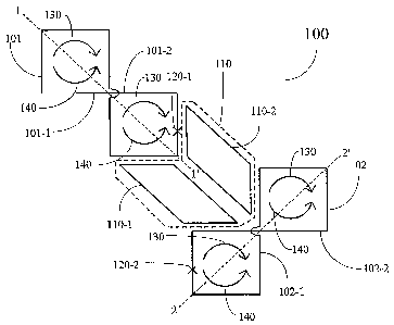
FIG. lA shows an embodiment of the present invention for coupling two
superconducting information devices using coupling device 110. In FIG. 1,
coupling
device 110 comprises two coupling elements 110-1 and 110-2 that are not in
electrical
communication with each other. This novel type of coupling, comprising two
coupling elements like in FIGS. 1 and 2, is referred to herein as the dual
coupling
scheme. In some embodiments, information devices 101 and 102 are flux devices,
and may have the same structure and size. In some embodiments of the
invention,
while information devices 101 and 102 have similar structures and sizes, they
are not
identical due to fabrication imperfections. In some embodiments of the present
invention, information devices 101 and 102 are gradiometric flux devices. In
some
embodiments of the present invention, other types of information devices 101
and 102
can be used. Information devices 101 and 102 in FIG. 1 A illustrate one
embodiment
of a gradiometric flux device, in which each device has one loop comprising
two
lobes (lobes 101-1 and 101-2 in information device 101, as well as lobes 102-1
and
102-2 in information device 102). Information devices 101 and 102 liave only
one
loop since the corners of the lobes are not electrically connected where they
meet in
FIG. 1. As illustrated in FIG. 1, the loop in information device 101 and the
loop in
information device 102 is interrupted by a Josephson junction 120, denoted by
an X.
The location of the Josephson junction in each loop can vary from information
device
to information device on a single chip and between chips. In some embodiments
of
21
CA 02593093 2007-06-28
WO 2006/069450 PCT/CA2005/001987
the present invention, the information devices comprise more than one
Josephson
junction.
Information devices 101 and 102 are coupled by coupling device 110 that is
placed diagonally between flux devices 101 and 102 as shown in FIG. 1A.
Coupling
device 110 applies an inductive coupling between information devices 101 and
102.
In some embodiments of the present invention, coupling device 110 comprise a
plurality of SQUIDs, such as dc-SQUIDs or rf-SQUIDs. Each element (e.g., rf-
SQUID or dc-SQUID) within coupling device 110 can be operated independently of
the others.
Using both elements 110-1 and 110-2, information devices 101 and 102 can be
controllably coupled. When coupling device 110 comprises dc-SQUIDs,
controllable
coupling can be obtained by applying a bias current to each respective
coupling
element (here each respective coupling dc-SQUID) or by changing the magnetic
flux
within the respective coupling element loops. When coupling device 110
comprises
rf-SQUIDs, controllable coupling is achieved by changing the magnetic flux
within
the SQUID loop of each respective coupling element. In some embodiments, one
coupling element in coupling device 110 is a dc-S QUID while the other
coupling
element is an rf-SQUID. In such embodiments, controllable coupling is achieved
by
applying a bias current or by changing the magnetic flux of the dc-SQUID and
by
changing the magnetic flux within the SQUID loop of the rf-SQUID.
Exemplary coupling elements 110 in accordance with some embodiments of
the present invention are illustrated in FIGS. IB and IC, In FIG. 1B, an
exemplary
coupling element 110 comprises an rf-SQUID that includes a loop of
superconducting
material 110-A interrupted by Josephson junction 110-B. In the embodiment
illustrated, controllable coupling is realized by controlling the magnetic
flux through
the rf-SQUID. The coupling element 110 of FIG. IB further includes a flux bias
source 110-C for threading magnetic flux through loop 110-A. In some
embodiments,
flux bias source 110-C comprises a loop of metal placed such that it is
inductively
coupled to superconducting loop 110-A. The coupling state of the coupling
element
can be controlled by varying the current in flux bias source I 10-C. When a
current is
applied to flux bias source 110-C a magnetic field results that threads
superconducting
loop 110-A. In some embodiments, the magnetic flux is useful for controlling
the
coupling state of coupling element 110 of FIG. 1B. In an embodiment of the
present
22
CA 02593093 2007-06-28
WO 2006/069450 PCT/CA2005/001987
invention, the magnetic flux ranges from -(Do to +(D0, where (Do is the flux
quantum.
In some embodiments, magnetic flux useful for controlling coupling element 110
of
FIG. 1B ranges from about -10*(DQ to about +10*(D0. The flux required to
control
coupling element 110 of FIG. I B depends on the characteristics of the device,
such as
the size of superconducting loop 110-A and the properties of Josephson
junction 110-
B. In some embodiments, superconducting loop 110-A has a size ranging from
about
1 square micron to about 10,000 square microns. In some embodiments, Josephson
junction 110-B has a size ranging from about 0.1 microns to about 50 microns.
In
some embodiments, superconducting loop 110-A is made out of niobium. In some
embodiments, superconducting loop 110-A is made of aluminum. In some
embodiments, superconducting loop 110-A is made of a superconductor fabricated
on
a silicon substrate.
FIG. 1 C illustrates another coupling element 110 in accordance with the
present invention. The coupling element 110 of FIG. 1 C comprises a DC-SQUID
that
includes a loop of superconducting material 110-A interrupted by two Josephson
junctions 110-B 1 and 110-B2. The coupling element 110 of FIG. 1 C further
includes
two bias leads 110-Cl and 110-C2 for applying a bias current through the
coupling
element 110. In some embodiments, the characteristics of the coupling element
110
of FIG. 1 C are substantially the same as those of the coupling element I 10
of FIG.
1B. Josephson junctions 110-B1 and 110-B2 can be the same size as Josephson
junction 110-B or different. The coupling element 110 of FIG. 1C can be
controlled
by applying a bias current across leads 110-C 1 and 110-C2 and also by a flux
bias
(which is not shown) similar to 110-C of FIG. 1B.
In some embodiments of the present invention, bias current magnitudes useful
for controlling the coupling of dc-SQUIDs of the present invention ranges from
about
I picoamperes (pA) to about 10 milliamperes (mA). One characteristic of
Josephson
junctions 110-B1 and 110-B2 is their critical current. The critical current of
a
Josephson junction is the magnitude of current beyond which the junction
begins to
break Cooper pairs. The critical current of a Josephson junction is also
defined as the
minimum current at which a resistance arises across the junction and,
conversely,
below which the junction is superconducting and has near-zero resistance. In
some
embodiments of the present invention, the bias current applied is less than
the critical
current of Josephson junctions 110-B1 and 110-B2.
23
CA 02593093 2007-06-28
WO 2006/069450 PCT/CA2005/001987
Each coupling element 110 of FIG. 1 has a dimensionless inductance, P =
27uLIcADo, where L is the inductance of the element, I,, is the critical
current of the
element, and cDo is the flux quantum. The dimensionless inductance can also be
written as (3 = L/Lj, where Ll = cDo/27i1c is called the Josephson inductance.
The value
of the dimensionless inductance determines the whether or not the coupling
element
110 is monostable ((3 < 1) or bistable ((3 > 1). Monostability means that the
potential
energy of the coupling element 110 only has one minimum, whereas bistability
means
that the potential energy has two minima. For the purposes of coupling, it is
preferable that coupling elements 110 are not bistable in the present
invention.
However, the lower (3 is, the lower the coupling strength, so (3 should not be
much less
than 1. In some embodiments of the present invention, the dimensionless
inductance
of coupling elements 110 is between 0.5 and 2. In some embodiments of the
present
invention, the dimensionless inductance of coupling elements 110 is between
0.7 and
1.5. In some embodiments of the present invention, the inductance of coupling
elements 110 is on the same order as their Josephson inductances, which means
the
dimensionless inductance is approximately one. In an embodiment of the present
invention, the first and second information devices have dimensionless
inductances
greater than one.
Referring to Fig. lA, in one embodiment of the present invention, coupling
device 110 is in close enough proximity to lobe 101-2 of information device
101 to
couple to the lobe. Coupling element 110-1 is in close proximity to lobe 102-1
of
information device 102 while coupling element 110-2 is in close proximity to
lobe
102-2 of information device 102. Herein, elements or devices are in close
proximity
to each other when the distance between the elements or devices (e.g., SQUIDs
or
loops of SQUIDs) is such that the coupling strength between the two elements
or
devices is non-negligible. A coupling strength is considered non-negligible
when it
can be measured using conventional measuring devices. In FIG. lA, coupling
device
110 is coupled to the same lobe of information device 101 but different lobes
of
information device 102. In some embodiments of the present invention, the
couplings
between the coupling elements of coupling device 110 and the information
device
lobes are all anti-ferromagnetic. However, there is no requirement that such
couplings be all anti-ferromagnetic. In some embodiments, the coupling between
information devices 101 and 102 can be either ferromagnetic or anti-
ferromagnetic.
24
CA 02593093 2007-06-28
WO 2006/069450 PCT/CA2005/001987
As noted above, in some embodiments, information devices 101 and 102 are
gradiometric flux devices. In some embodiments, gradiometric flux devices that
can
be used in quantum computing architectures such as disclosed in Fig. 1A have
two
configurations in each lobe. Using Fig. 1A for reference, these configurations
correspond to clockwise 130 and counterclockwise 140 currents circulating
around
each lobe. The direction that clockwise 130 or counterclockwise 140 current
would
flow, when present, is shown in each lobe of the information devices depicted
in FIG.
IA. However, illustration of the direction of such currents is not to be
construed to
mean that such currents are always present in these lobes.
Information devices 101 and 102 in FIG. lA have different current
configurations in each lobe, since the information devices are made of one
loop of
superconducting material. For example, in information device 101, lobe 101-1
can
have clockwise circulating current 130 while lobe 101-2 has counterclockwise
circulating current 140, or vice versa. Conversely, for example, in
information device
101, lobe 101-1 can have counter-clockwise circulating current 140 while lobe
101-2
has clockwise circulating current 130. The same applies to information device
102.
Thus, by using coupling elements 110, lobe 101-2 of information device 101 can
be
coupled to a lobe of information device 102, which either has the same or
opposite
direction of circulating current. Depending on whether the coupled current
directions
are the same or opposite, ferromagnetic or anti-ferromagnetic coupling is
achieved.
For example, consider the case in which lobe 101-2 has a clockwise 130
circulating
current configuration and thus lobe 101-1 has counterclockwise 140 circulating
current. Further, in some embodiments, lobe 102-1 has clockwise 130
circulating
crurent and lobe 102-2 has counterclockwise 140 circulating current. Thus,
when
coupling element 110-1 is turned on while coupling element 110-2 is turned
off,
information device 101 is ferromagnetically coupled to information device 102.
When, on the other hand, coupling element 110-2 is on while coupling element
110-1
is off, then flux device 101 is anti-ferromagnetically coupled to information
device
102. Thus, in this manner, switching the on/off status of coupling elements
110-1 and
110-2 can effect switching of the coupling type of information devices 101 and
102
between anti-ferromagnetic coupling and ferromagnetic coupling, and vice
versa.
In the example above, coupling elements in coupling device 110 can also be
biased in such a way that coupling element 110-1 provides anti-ferromagnetic
coupling and coupling element 110-2 provides ferromagnetic coupling. In some
CA 02593093 2007-06-28
WO 2006/069450 PCT/CA2005/001987
embodiments of the present invention, coupling device 110 can be biased so
that both
elements provide only either ferromagnetic or anti-ferromagnetic coupling.
In preferred embodiments, when both coupling elements 110-1 and 110-2 are
off, information devices 101 and 102 are not coupled to each other.
Information
devices 101 and 102 can share some flux through their lobes, but the general
orthogonality of the information devices in FIG. 1, illustrated by lines 1-1'
and 2-2',
prevents coupling between them. For example, lobe 101-2 in infonnation device
101
can be inductively coupled directly to lobes 102-1 and 102-2. The strength of
this
coupling is approximately proportional to r Z, where r is the inter-lobe
distance. Here,
inter-lobe distance between two lobes is defined as the distance between the
centers of
the two lobes. When the coupling strength of coupling device 110 is set to
zero, lobe
101-2 will be anti-ferromagnetically coupled to both lobes of information
device 102.
However, these two couplings are equal in strength and therefore cancel each
other
out resulting in a net coupling strength of zero, assuming that the physical
parameters
of information devices 101 and 102 are the same. However, due to differences
in the
physical parameters of information devices 101 and 102 (e.g., arising, for
example, as
a result of imperfections in device fabrication), the coupling between
information
device 101-2 and one lobe of flux device 102 might be slightly stronger than
the
coupling between lobe 101-2 and the other lobe of information device 102.
Consequently an appreciable residual coupling may exist between devices 101
and
102. This residual coupling can be made smaller by spacing devices 101 and 102
farther apart, thereby increasing r.
When both coupling elements 110-1 and 110-2 are on, coupling cancellation is
also possible. In this case, coupling device 110 will facilitate ferromagnetic
and anti-
ferromagnetic couplings. These couplings can be tuned so that they are of
equal
strength and can thus be cancelled out. Tuning a coupling comprises tuning the
individual the coupling elements, which can be SQUIDs in some embodiments of
the
present invention. This tuning can also work when the flux devices are not
exactly
the same (e.g. due to imperfections in fabrication). In the case where the
couplings
are not exactly equal, a small residual coupling can exist between the flux
devices. In
some embodiments of the present invention, the coupling device 110 is biased
in such
a way as to cancel out all residual coupling in the system and therefore leave
information devices 101 and 102 completely uncoupled. In other words, the
strength
26
CA 02593093 2007-06-28
WO 2006/069450 PCT/CA2005/001987
of coupling device 110 can be tuned to cancel out the residual coupling
described
above.
Coupling elements 110-1 and 110-2 can also be on for reasons other than
coupling cancellation. In some embodiments of the present invention, when both
coupling elements are on, one coupling element can be used to couple
information
devices 101 and 102, while the other coupling element can be used to induce a
local
magnetic field that can be used to bias one of the information devices. In
some
embodiments of the present invention, coupling device 110 can also be used to
read
out the state of an inforniation device to which it is coupled.
In some embodiments of the present invention, the coupling strength between
infonnation devices 101 and 102 is tunable. That is, by changing bias
conditions on
either coupling element 110-1 or 110-2, the strength of the ferromagnetic or
anti-
ferromagnetic coupling between information devices 101 and 102 can be
adjusted. In
the Hamiltonian of system 100, 6Z az represents the "sigma z" coupling
between
information devices 101 and 102 and Jis a pre-factor that indicates the
strength of the
interaction between information devices 101 and 102. When J> 0, the coupling
between information devices 101 and 102 is anti-ferromagnetic, with a higher J
meaning a stronger anti-ferromagnetic coupling. When J < 0, the coupling
between
flux devices 101 and 102 is ferromagnetic, with a lower J meaning a stronger
ferromagnetic coupling. When J = 0, coupling devices 110 provide no additional
coupling between information devices 101 and 102. In some embodiments of the
present invention, the coupling strength of coupling devices can be
continuously or
nearly continuously varied from J= 1 to J=-1 by appropriate tuning of coupling
device 110.
Coupling elements 110-1 and 110-2 can also inductively couple to each other.
However, such coupling is negligible to operation of system 100. In some
embodiments of the present invention, coupling elements 110-1 and 110-2 are
fabricated in order to minimize inductive coupling between them.
FIG. 2 shows another embodiment of the present invention. In some
embodiments in accordance with FIG. 2, information devices 201 and 202 of
system
200 are flux devices. In fact, in FIG. 2, information devices 201 and 202 are
depicted
as gradiometric flux devices and are arranged in a regular grid pattern rather
the
diagonal pattern of FIG. 1. Information devices 201 and 202 both have two
lobes
27
CA 02593093 2007-06-28
WO 2006/069450 PCT/CA2005/001987
that each hold a circulating current configuration and at least one Josephson
junction
220. The direction that clockwise 130 or counterclockwise 140 current would
flow,
when present, is shown in each lobe of the device depicted in FIG. 2. However,
illustration of the direction of such currents is not to be construed to mean
that such
current is always present in these lobes.
Information devices 201 and 202 differ from the information devices of FIG. I
in that information devices 201 and 202 are not made from one continuous loop.
Instead, in both information device 201 and 202, a central leg, which includes
at least
one Josephson junction 220, connects two opposite points on a loop. Thus, in
information device 201, there is no constraint imposed on the direction of
current flow
in lobe 201-1 relative to lobe 201-2. Likewise, in information device 202,
there is no
constraint imposed on the direction of current flow in 202-1 relative to lobe
202-2. In
contrast, in the lobes of information devices 101 and 102, current can only
flow in
opposite directions in their two lobes. In some embodiments of the present
invention,
the central leg of each information device (201 and 202) comprises a dc-SQUID
that
includes two Josephson junctions.
In a preferred embodiment of the present invention in accordance with FIG. 2,
information devices 201 and 202 have currents that flow in opposite directions
in their
respective lobes. That is, each information device has opposing currents in
its two
lobes, which can be used to represent the eigenstates, or quantum states, of
the
information device. Since the physical states of system 200 have currents of
this
form, a dual coupling scheme can be applied to this type of information device
as
described below.
Coupling elements 110-1 and 110-2 couple flux devices 201 and 202 together.
The operation of system 200 is equivalent to that of the system depicted in
FIG. 1.
That is, when lobes 202-1 and 202-2 have opposite current configurations, lobe
201-2
can be ferromagnetically or anti-ferromagnetically coupled to flux device 202.
This is
done by switching the coupling elements 110-1 and 110-2 on or off as described
previously in conjunction with FIG. 1.
It can be appreciated that flux devices other than flux device 101 or flux
device 201 can be used in the dual coupling scheme presented above. In a
preferred
embodiment of the present invention, the type of information device used in
the dual
coupling scheme is a gradiometric flux device. In some embodiments of the
present
invention, the information device used in the dual coupling scheme is another
type of
28
CA 02593093 2007-06-28
WO 2006/069450 PCT/CA2005/001987
flux device. It can also be appreciated that the shape of coupling elements
110-1 and
110-2 is not restricted to the shapes depicted in FIGS. I and 2.
FIG. 3 shows a schematic integrated circuit of a two-dimensional (2D) array
300 of information devices 101 and 102 coupled to their nearest neighbors
using the
dual coupling scheme described above in conjunction with FIG. 1. Array 300 is
an
expansion of system 100 of FIG. 1. Information devices 101 and 102 in array
300 are
depicted as gradiometric flux devices, but other flux devices can be used as
well. Each
device in the interior of the array is coupled to four neighboring devices. In
accordance with the present invention, by switching the different coupling
elements
on and off, a device in array 300 can ferromagnetically or anti-
ferromagnetically
couple to any one of its neighbors. In some embodiments of the present
invention, a
Hamiltonian of a problem to be solved can be mapped onto the array of devices.
Array 300 can thereby simulate the Hamiltonian and provide infonnation about
or a
solution to the problem. In some embodiments of the present invention, array
300 is
designed to solve only one Hamiltonian.
FIG. 4 shows a 2D array 400 of information devices coupled together using
the dual coupling scheme described above in conjunction with FIG. 2. Array 400
is
an expansion of the system depicted in FIG, 2 and operates in the same way.
Each
device in the interior of array 400 can be coupled ferromagnetically or anti-
ferromagnetically to all four of its nearest neighbor devices.
It can be appreciated that while arrays 300 and 400 are specific embodiments
of 2D arrays of information devices that employ the dual coupling scheme
described
above, other types of arrays are possible. For example, in an embodiment of
the
present invention, a 2D array of information devices with dual coupling to
three
nearest neighbors is possible. In some embodiments of the present invention,
the
number of coupled neighbors is greater than four. In some embodiments of the
present invention, the array is a linear array and each information device is
coupled to
its two nearest neighbors. In sotne embodiments, the 2D array of information
devices,
such as those illustrated in FIGS. 3 and 4, comprise between ten and ten
thousand
devices, more than fifty devices, more than 100 devices, or less than two
thousand
devices.
29
CA 02593093 2007-06-28
WO 2006/069450 PCT/CA2005/001987
Tunable Flux Transformers
In an aspect of the present invention, coupling devices for coupling
information devices ferromagnetically and anti-ferromagnetically comprise only
one
coupling element. In particular, a monostable rf-SQUID or a dc-SQUID can
mediate
an inductive coupling between two adjacent information devices. The nontrivial
dependence of the SQUID's susceptibility on external flux makes it possible to
continuously tune the induced coupling from anti-ferromagnetic to
ferromagnetic. In
particular, for suitable parameters, the induced ferromagnetic coupling can be
sufficiently large to overcome any possible direct anti-ferromagnetic
inductive
coupling between the information devices. In some embodiments of the present
invention, a single rf-SQUID or a single dc-SQUID is used to couple two
information
devices together in a way that allows the type of coupling to be switched from
ferromagnetic to anti-ferromagnetic or vice versa. In some embodiments of the
present invention, the information devices are flux devices, such as rf-SQUIDs
or
persistent ctirrent qubits.
FIG. 5 illustrates three rf-SQUIDs 510-a, 510-b, and 510-c. Each rf-SQUID
consists of a loop of superconducting material interrupted by a Josephson
junction
(denoted by an X in the loop). These rf-SQUIDs are depicted in a row for
convenience. In FIG. 5, rf-SQUID 510-b is a controllable coupling switch and
is
disposed between rf-SQUID 510-a and rf-SQUID 510-c. In an embodiment of the
present invention, rf-SQUID 510-b can be replaced with a general coupling
switch or
coupling device for controlling the coupling interaction between rf SQUIDs 510-
a
and 510-c. An example of a general coupling switch is a flux transformer. The
rf-
SQUIDs couple to each other inductively. In some embodiments of the present
invention, rf-SQUIDs 510-a and 510-c are used as information devices. The rf-
SQUIDs 510 have circulating superconducting cturent as well as associated
flux,
which can be labeled by its direction, such as ~ and T.
In embodiments of the present invention, rf-S QUID 510-b is monostable,
meaning that the potential energy of the rf-SQUID only has one minimum. This
can
be achieved either by biasing rf-SQUID 510-b with a flux close to an integer
number
of quanta for a dimensionless inductance less than a critical value defined by
the
Josephson junction of rf-SQUID 510-b or for any flux bias by making rf-SQUID
510-
b such that the dimensionless inductance is around 1 or less than 1. The
CA 02593093 2007-06-28
WO 2006/069450 PCT/CA2005/001987
dimensionless inductance is defined as (3b = 4e2 LbEb (here, h =1; in SI
units, P =
2nLI,/(Do), where Lb is the inductance and Eb is the Josephson energy of rf-
SQUID
510-b. This value of the dimensionless inductance can be achieved by reducing
Eb
while keeping the area of the loop of rf-SQUID 510-b, and hence the inductive
coupling, appreciable. The inductive coupling is considered appreciable when
it
produces a measurable effect on a device coupled to it. In some embodiments of
the
present invention, the area of the loop of rf-SQUID 510-b ranges from about I
square
micron to about 10,000 square microns. Reducing Eb corresponds to reducing the
critical current of rf-SQUID 51-b. For example, reduction in the critical
current can
be accomplished by reducing its critical current density during manufacturing,
or by
reducing the cross-sectional area of the Josephson junction in the rf-SQUID.
In some
embodiments, the critical current of the rf-SQUID is between about I pA and
about
10 mA. When required, a shunting capacitance can be placed across the
Josephson
junction in rf-SQUID 510-b to keep the rf-SQUID in the flux regime.
In an embodiment of the present invention, rf-SQUID 510-b has a
dimensionless inductance slightly less than one to ensure monostability and a
strong
coupling. In an embodiment of the present invention, rf-SQUID 510-b has a
dimensionless inductance between 0.7 and 1. In another embodiment of the
present
invention, rf-SQUID 510-b has a dimensionless inductance between 0.8 and 1. In
yet
another embodiment of the present invention, rf-SQUID 510-b has a
dimensionless
inductance between 0.5 and 2. In another einbodiinent of the present
invention, rf-
SQUID 510-b has a dimensionless inductance between 0.9 and 1.1. In an
embodiment of the present invention, rf-SQUIDs 510-a and 510-c have
dimensionless
inductances greater than 1 but less than 2.
FIG. 6 shows a graph 600 modeling the total flux of an rf-SQUID, such as rf-
SQUID 510-b, versus the applied external flux (~b versus 0b ). Such a graph is
hereinafter named the S-curve. The axes of FIG. 6 are in dimensionless phase
units,
~, and this is expressed in terlns of the applied magnetic flux as ~=
2n*((D/(Do), where
(D is the applied external flux or total flux depending on the respective axis
of FIG. 6.
The external flux is applied to the rf-SQUID loop, and the difference between
the
total and external flux is manifested by the current in the rf-SQUID. For
example,
curve 610 corresponds to the case wliere inductance is zero ((3b = 0), and is
a 45
degree line as expected for an open loop.
31
CA 02593093 2007-06-28
WO 2006/069450 PCT/CA2005/001987
Curve 620 in FIG. 6 represents the case in which inductance of rf-SQUID 510-
b is significantly less than 1((3b << 1) but is not zero. If flux device 510-a
flips from
T to ~, then, due to the mutual inductance between SQUIDs 510-a and 510-b,
this
effectively increases the external flux of rf-SQUID 510-b. For an external
flux near
zero , the S-curve has slope less than one so that this increase gets
partially shielded
by rf-SQUID 510-b's self-flux in the ~ direction. Thus, in such circumstances,
rf-
SQUID 510-b acts as a~-bias for flux device 510-c. Thus rf-SQUID 510-b
provides
anti-ferromagnetic coupling between rf-SQUIDs 510-a and 510-c in this case.
When,
in contrast, the external flux of rf-S QUID 510-b is close to (D0/2, the
physical
properties of rf-SQUID 510-b work in the opposite manner. There, the S-curve
has
slope greater than 1 (see curve 620 of FIG. 6) so that the self-flux does not
shield at
all but actually cooperates with the increase in external flux. Thus, the
coupling of rf-
SQUID 510-b changes sign to ferromagnetic.
In an embodiment of the present invention, an rf-SQUID coupler is configured
to provide ferromagnetic or anti-ferromagnetic coupling by applying an
external
magnetic field to the rf-SQUID coupler. In an embodiment of the present
invention,
the external magnetic field has a flux close to zero and the coupling is anti-
ferromagnetic. In an embodiment of the present invention, the magnetic field
has a
flux close to 00/2 and the coupling is ferromagnetic. In an embodiment of the
present
invention, a flux bias device is inductively coupled to the rf-SQUID coupler
and the
flux bias device provides the external magnetic field described above. In some
embodiments of the present invention, a magnetic field is applied to the
coupling
device that is between about -5*(Do and about +5*(D0, with an accuracy of
about
0.1 *(Do, where (Do is the flux quantum and (Do = 2.067 x 10⁻¹⁵ Webers (Wb).
In some
embodiments, the accuracy is 0.2*00 or lower.
FIG. 7 illustrates two information devices 710-a and 710-c coupled by dc-
SQUID 710-b. Information devices 710-a and 710-c as shown in FIG. 7 are rf-
SQUIDs, but they can be any other flux-based information device. Dc-SQUID 710-
b
comprises two Josephson junctions in a superconducting loop with two terminals
711
located between the junctions. While rf-SQUID coupler 510-b of FIG. 5 has only
a
flux bias, dc-SQUID coupler 710-b of FIG. 7 can be flux biased or current
biased.
Current bias can be provided by applying a current to dc-SQUID 710-b through
32
CA 02593093 2007-06-28
WO 2006/069450 PCT/CA2005/001987
terminals 711. Flux bias can be applied by an inductive current loop in close
proximity to the loop of the dc-SQUID.
Appropriate current and flux bias tuning can mediate the coupling provided by
dc-SQUID 710-b in order to controllably tune the strength of the coupling,
turn the
coupling off, or switch the sign of the coupling. Consider the case in which
the
external current bias on dc-SQUID 710-b is denoted lb and the external flux
bias is
denoted o6 . Further Pb is much less than 1(however, the case can be extends
to
higher values of (3b). When the dc-SQUID is symmetric, meaning that it has
identical
or near-identical Josephson junctions, the dc-SQUID can provide ferromagnetic
coupling provided that cos2(Ob /2) < I Ib/2I,1 < I cos(ob /2) 1, where Ic is
the critical
current of the Josephson junctions in dc-SQUID 710-b. If the flux bias was
zero, then
there is no value of the current bias that would provide ferromagnetic
coupling. Anti-
ferromagnetic coupling is achieved when cos2(0b /2) > 1 Ib/2I,, I . When cosa(
Ob /2)
= I Ib/2I, 1, the coupling is equal to zero. Thus, for a symmetric dc-SQUID,
both
current bias and flux bias are needed in order to switch the sign of the
coupling.
FIG. 8 illustrates the graph of the inequalities for the symmetric dc-S QUID
case in the limit of (3b much less than one, corresponding to the calculations
above.
The horizontal axis is the external flux bias oe , while the vertical axis is
the
normalized external current bias lb/2I,,. Curve 801 is the lower limit cos2(Ob
/2),
while curve 802 is the upper limit cos(ob /2). Thus, the area of the graph
inside
curve 801 represents the range of flux and current bias that will provide anti-
ferromagnetic coupling, with the area close to the origin having the strongest
anti-
ferromagnetic coupling. Curve 801 itself represents the contour of flux and
current
bias that result in zero coupling. The area bounded by curves 801 and 802
represents
the range of flux and current bias that will provide ferromagnetic coupling.
As the
flux and current bias moves away from curve 801 toward curve 802, the
ferromagnetic coupling becomes stronger. However, once the bias reaches curve
802
itself, the Josephson junctions switch into the voltage state and the
ferromagnetic
coupling becomes unstable. Therefore, the bias on the dc-SQUID coupler should
not
pass outside curve 802. As can be seen, a nonzero flux bias (Ob ~ 0) is needed
for
ferromagnetic coupling.
33
CA 02593093 2007-06-28
WO 2006/069450 PCT/CA2005/001987
For an asymmetric dc-SQUID, a current bias is not necessary to tune the
strength and sign of the coupling, since the flux bias alone can switch the
sign of the
coupling. As an example, when one of the Josephson junctions in the dc-SQUID
is
shorted out (e.g. its Josephson energy is infinite), then the dc-SQUID is
essentially an
rf-SQUID, which has been previously shown to have the ability to switch the
sign of
the coupling without the use of a current bias. In some embodiments of the
present
invention, dc-SQUID coupler 710-b is symmetric and has both a current and flux
bias.
In some embodiments of the present invention, dc-SQUID coupler 710-b is
asymmetric and only has a flux bias. In some embodiments of the present
invention,
dc-SQUID coupler 710-b is also configured to read out the state of either
information
device 710-a and 710-c.
In an embodiment of the present invention, dc-SQUID 710-b has a
dimensionless inductance slightly less than one to ensure monostability and a
strong
coupling. In an embodiment of the present invention, dc-SQUID 710-b has a
dimensionless inductance between 0.7 and 1. In another embodiment of the
present
invention, dc-SQUID 710-b has a dimensionless inductance between 0.8 and 1. In
yet
a.nother embodiment of the present invention, dc-SQUID 710-b has a
dimensionless
inductance between 0.5 and 2. In another embodiment of the present invention,
dc-
SQUID 710-b has a dimensionless inductance between 0.9 and 1.1. In an
embodiment of the present invention, rf-SQUIDs 710-a and 710-c have
dimensionless
inductances greater than 1 but less than 2.
In some embodiments of the present invention, when the coupling device (rf-
SQUID 510-b or dc-SQUID 710-b) in either FIGS. 5 or 7 is turned off, there is
no
coupling between the inforination devices (510-a and 510-c, or 710-a and 710-
c). In
some embodiments of the present invention, there is still direct inductive
coupling
between the information devices when coupling device is off. In this case, the
coupling device can be tuned to specific values using a flux bias device or
current bias
device to cancel out the direct inductive coupling to zero.
In some embodiments of the present invention, an array of information devices
uses tunable flux transformers, such as rf-SQUID 510-b or dc-SQUID 710-b, as
coupling devices. In an embodiment of the present invention, the array of
information
devices is two-dimensional and each device in the interior of the array is
coupled to
its four nearest neighbor flux devices using rf-SQUID or dc-SQUID couplers. In
an
embodiment of the present invention, the array of information devices is a one-
34
CA 02593093 2007-06-28
WO 2006/069450 PCT/CA2005/001987
dimensional chain with the rf-SQUID or dc-SQUID couplers disposed between each
device. It can be appreciated that other arrangements of the array of
information
devices and their respective couplers are possible.
Dif ectJosephson junction coupling
In an aspect of the present invention, one or more Josephson junctions
galvanically
coupled (e.g., inductively coupled or capacitively coupled) to two information
devices can
tunably couple the two information devices together. This tunable coupling can
switch the
sign of the coupling from ferromagnetic to anti-ferromagnetic and vice versa.
In some
einbodiments of the present invention, a plurality of information devices are
coupled
together using galvanically connected Josephson junctions.
FIG. 9 shows a system 900 that employs such direct Josephson junction
coupling.
Information devices 901 and 902 are flux devices comprising three Josephson
junctions in
a superconducting loop, but need not be restricted to such an architecture.
Coupling
device 910 comprises four Josephson junctions arranged in a cross-loop design
that
galvanically couple flux devices 910 and 902 together. Coupling device 910
also
comprises four wires 911 that can provide a current bias for the coupling
device. The
Josephson junctions in coupling device 911 are large in size compared to the
Josephson
junctions of flux devices 901 and 902. In an embodiment of the present
invention, there is
no magnetic flux threading the coupling device 910, which means that the cross-
wires of
coupling device 910 are fabricated to be almost on top of each other, but on
different
layers.
Let the external current bias in the wires 911 be denoted Il, IZ, 13, and Ia
for wires
911-1, 911-2, 911-3, and 911-4 respectively. There is a wide range of
tunability for wires
911, but the suin of currents in the four wires must be equal to zero during
operation of
coupler 910 as a coupling device. Current can flow througli the cross-wires of
the
coupling device (911-1 to 911-4 or vice versa; 911-2 to 911-3 or vice versa)
or through the
horizontal wires of the coupling device (911-1 to 911-2 or vice versa; 911-3
to 911-4 or
vice versa). Depending on how the wires are biased, both ferromagnetic and
anti-
ferromagnetic coupling can be produced. Current flowing through the cross-
wires
produces an anti-ferroinagnetic coupling while current flowing through the
horizontal
wires produces a ferromagnetic coupling.
Two useful sets of current configurations arise. The first is 11 = I2 = I3 =
I~ = I,
where I is an arbitrary current value that is between zero and the critical
current of the
CA 02593093 2007-06-28
WO 2006/069450 PCT/CA2005/001987
Josephson junctions in coupling device 910. The magnitude of I determines the
strength
of the coupling. When biased in this manner, no current flows through the
cross wires but,
rather, current flows through the horizontal wires. In this current
configuration, the
ferromagnetic interaction dominates over the anti-ferromagnetic interaction,
and therefore
=
flux devices 901 and 902 are coupled ferromagnetically. The second
configuration is 11
IZ = I3 = I4 = I. In this scenario, the current flows through the cross-wires
and not
through the horizontal wires. This produces a net anti-ferromagnetic coupling
between
flux devices 901 and 902. Tlhus, by appropriate current bias of wires 911,
coupling device
910 can mediate switching of the sign of the coupling between flux devices 901
and 902.
In some embodiments of the present invention, not all the current bias in
wires 911
have to have the same magnitude, but must maintain the correct sign. If the
current bias
magnitudes are close but not equal in magnitude, then current will flow in
both the cross-
wires and horizontal wires, creating both a ferromagnetic coupling component
and an anti-
ferromagnetic coupling component. However, the sign of the current bias will
ensure that
the coupling device will have a dominant preference for the flow of current
and therefore
one type of coupling will typically dominate the other in strength. In some
embodiments
of the present invention, the current bias of wires 911 can tune the coupling
strength by
appropriate tuning of the individual biases. In some embodiments of the
present invention,
the current bias of wires 911 can be chosen to provide zero coupling between
two
information devices.
FIG. 10 shows a system 1000 that includes another embodiment of direct
Josephson junction coupling. In FIG. 10, boxes 1001 and 1002 represent
information
devices and can have many different architectures. For example, one embodiment
of an
information device 1001 and/or 10002 is the three Josephson junction flux
device 901 (and
902) illustrated in FIG. 9.
Coupling device 1010 comprises three Josephson junctions 1010-1, 1010-2, and
1010-3 in a superconducting loop galvanically connected to both information
devices 1001
and 1002. With appropriate tuning, coupling device 1010 can provide both
ferromagnetic
and anti-ferromagnetic coupling between the information devices. Coupling
device 1010
is biased through its superconducting loop by an external flux bias 0e . The
Hamiltonian
of the interaction between the information devices when using coupling device
1010 is
_ E2 cos ~Ib (25)
H,nt - 4eaE,E3 IuI~
36
CA 02593093 2007-06-28
WO 2006/069450 PCT/CA2005/001987
where Ej is the Josephson energy of Josephson junction 1010-1 (EI),1010-2
(E2), or 1010-
3 (E3), IQ is the critical current of flux device 1001, and lb is the critical
current of flux
device 1002. Therefore, depending on the value of the external flux bias, the
sign of the
interaction can be switched from positive to negative or vice versa. This is
the same as
switching from anti-ferromagnetic to ferromagnetic and vice versa. Also, the
magnitude
of the coupling interaction can be tuned by tuning the external flux bias and
can be made
zero for certain values of the bias. The coupling strength is maximum when I
cos 0b (=
1, which corresponds to 0b being an integer multiple of ~. The coupling
strength is zero
when cos ob = 0, which corresponds to ob being a multiple of either 7/2 or
37c/2.
In some embodiments of the present invention, a plurality of information
devices
are coupled together using a plurality of direct Josephson junction coupling
devices.
Examples of such devices are device 910 in FIG. 9 and device 1010 in FIG. 10.
In some
embodiments of the present invention, both coupling devices 910 and 1010 are
used in the
same circuit. In some embodiments of the present invention, the plurality of
flux devices
comprises a two-dimensional grid with flux devices coupled to their nearest
neighbors
using direct Josephson junction coupling devices. In other embodiments, the
plurality of
flux devices comprise a one-dimensional chain with flux devices coupled to
their nearest
neighbours using direct Josephson junction coupling devices.
Variations in Fabrication of Coupling Devices
It can be appreciated that there are many ways to fabricate the various
embodiments of the invention. These methods of fabrication are well known in
the art.
Examples of such art have been incorporated by reference in the background
section of the
specification.
One specific fabrication embodiment that can be enlployed with the present
invention is the concept of fabricating a coupling device utilizing two
layers. Normally,
the superconducting loop of a coupling device such as rf-SQUID 510-b of FIG. 5
and dc-
SQUID 710-b of FIG. 7 are fabricated on a single layer of a superconducting
chip. That is,
the superconducting loop is solely contained on one layer of the circuit. A
superconducting loop fabricated in this manner may take up a considerable
amount of
available surface area (real estate) on the chip where no other wires or
devices can be
placed. Also, such a design is not fully advantageous because there exists a
parasitic
37
CA 02593093 2007-06-28
WO 2006/069450 PCT/CA2005/001987
capacitance between the superconducting loop and surrounding elements of the
chip.
Thus, surrounding elements need to be positioned away from the superconducting
loop,
which takes up even more of the available surface area (real estate) on the
chip. To
address these drawbacks, in some embodiments of the present invention, a
section of the
superconducting loop of a coupling device is fabricated on a separate layer on
the chip.
For example, rf-SQUID 510-b is fabricated such that it comprises two small
open loops on
a first layer of the chip coupled to SQUIDS 510-a and 510-c. These open loops
are
connected to each other by two microstrip wires, one oii the same layer as the
open loops,
and another on a second layer connected to the first layer by vias, thus
creating one
continuous closed loop that couples SQUIDs 510-a and 5109-c together. A
Josephson
junction is present in one of the strips. In some embod'unents, the two
microstrips are
fabricated with one directly above the other. In some embodiments, the second
layer is a
ground plane of a chip. In some embodiments, a plurality of coupling devices
is fabricated
in this manner with one open loop from each of the coupling devices occupying
one layer
and another open loop from each of the coupling devices occupying another
layer in the
plurality of coupling devices.
When the coupling devices are fabricated in this manner, the available
horizontal
surface area on the chip (real estate) that is taken up by the coupling device
is reduced,
since the superconducting loop of the coupling device has effectively been
turned
vertically. Thus more devices can be placed on the chip. This fabrication
inethod does not
prohibit the resultant coupling devices froin operating in the fashion
described in the
present invention. Also, this configuration reduces the amount of parasitic
capacitance that
from the superconducting loops in the coupling devices. What follows are
detailed
analytical examples of the couplings that the dcSQUID and rf-SQUID can
facilitate
between two rf-SQUID flux devices.
Example 1- Tunable coupling offlux devices through an Yf-SQUID transformer
FIG. 5 illustrates how the dynamics of three rf-SQUIDs 510-a, 510-b, and
510-c, including the tunability of the sign of coupling, can be modeled by an
analysis
beginning at the classical potential of the rf-SQUIDs. In this example, a, b,
c-SQUID
or a, b, and c denote rf-SQUIDs 510-a, 510-b, and 510-c, respectively.
Hereafter, in
this example a, b, and c as a superscript, subscript, or connected to a value
or term by
a hyphen denotes a value in relation to rf-SQUIDs 510-a, 510-b, and 510-c.
Values
and quantities drawn to these rf-SQUIDs include but are not limited to:
38
CA 02593093 2007-06-28
WO 2006/069450 PCT/CA2005/001987
L, the rf-SQUID inductance;
B, the dimensionless SQUID inductance (defined to be equal to 2nLI,/(Do in SI
units, when b= 1 this becomes 4e2LE);
C, the rf-SQUID capacitance;
I., the critical current of the rf-SQUID;
E, the rf-SQUID Josephson energy (defined to be ~ Ic);
Ij, the current of rf-SQUID 510 j, where j= a, b, or c;
cDj , the flux of rf-SQUID 510-j, where j= a, b, or c;
Ol, the dimensionless flux, where j= a, b, or c;
cp', the dimensionless external flux 'X' applied to rf-SQUID 510 j, where j=
a, b, or c;
0 tot, the total flux of an rf-SQUID,
M;j, the mutual inductance, where i, j= a, b, or c, etc.
As shown, in FIG. 5, three rf-SQUIDs 510-a, 510-b, and 510-c are considered.
The rf-SQUIDs 510-a and 510-c are degenerately biased flux devices, while 510-
b rf-
SQUID is a coupling element, tunable by an external flux bias (not shown). To
obtain
indirect coupling between information devices 510-a and 510-c, it suffices to
consider
the potential:
U = -.E,,, cos 0,s - Eb cos -ob - E,, cos ~G 4- 8~8ry ~~ r ~~-SS~~) f l~)
~.
with the inductance matrix
La - -A-I,~b 0
L = -JW.b. Lb -Mb. (2)
0 -Mb, LG
That is, the direct anti-ferromagnetic inductive 510-a to 510-Oc coupling is
assumed to be
small. This can be achieved, for example, through the use of gradiometric
information
devices described above. However, as long as M. is small, an interaction term
Ma,lal, can
be added to the final result (9) below. In accordance with the roles played by
the various
loops, as previously described, in some embodiments the flux biases are chosen
as
39
CA 02593093 2007-06-28
WO 2006/069450 PCT/CA2005/001987
~+
q5xb (~)
7' + 0'b-~)
where, ~p X is a column vector with elements 0a ,0b , and OX. Thus, 0a
compensates
externally for the shielding flux that loop 510-b couples into the a- and c-
SQUIDs. See
equation (6) below for a def nition of 0b .
If the b-SQUID is to act as a passive coupler without introducing additional
degrees of freedom, the b-SQUID should not be bistable. Therefore, in
embodiments of
the present invention where there is an rf-SQUID acting as a coupler, the rf-
SQUID is
preferably monostable. Monostability can be achieved either by biasing the rf-
SQUID
with a flux close to an integer number of quanta (oe small), or for any flux
bias by
making the rf-SQUID such that the dimensionless inductance is less than one.
That is,
/jb = 4e2Lb Eb < 1 (here, h = 1; in SI units, 0 = 27rLId(Do). This
dimensionless inductance
value can be acliieved by reducing Eb while keeping the area of the b-loop,
and hence the
inductive coupling, appreciable. Reducing the critical current density of the
Josephson
junction during manufacturing, or the cross-sectional area of the Josephson
junction in the
rf-SQUID, corresponds to reducing the critical current of the rf-SQUID. In
some
embodiments a shunting capacitance is placed across the Josephson junction in
rf-SQUID
510-b in order to keep the b-SQUID in the flux regime. The calculation that
follows is
valid in either case, and their relative merits will be discussed afterwards.
In addition, even
a SQUID with a unique potential minimum will have excited states,
corresponding to
plasma oscillations. While these are outside the scope of the present
semiclassical
analysis, the corresponding excitation energies should be different from any
transition in
the a- and c-devices if the b-SQUID is to remain passive.
Proceeding by expansion in M. Without suggesting that the regime of M/L is
much less than 1(say, distant loops) is the most practical, this leads to a
transparent result,
which can guide numerical studies in the general case. The b-mediated a-c
coupling is
expected to be OPP) so the junction phases will be written as
-I- ~j f- ~(11 la~ ~ ~~)
CA 02593093 2007-06-28
WO 2006/069450 PCT/CA2005/001987
and can be determined by solving the equilibrium condition V i = 0. In leading
order,
these are just the stationary phases of an isolated rf-SQUID,
r3a sin 4 -}- (p) j -- ar = 0 U -- ax a) (5)
,13b sin ob + Ob -- o-bc = 0 , (6)
where ~-7c can have either sign. The inverse inductance matrix is needed to
the same
order
1 ILv -I-1Jr~blIF~Lb 1ff.blLaLb 1Jfab.tYlb.1L=aLbLa
lL'~ = M,,b/L,~Lb 1lLb 11b./LbLa + o(m3) .
1 1Le 4- AlilLbLa
(iJ
Use of (7) consistently leads to significant cancellations as described below.
in ~(M), one finds that x,,, = 0 due to the special choice of i X in (3),
while the
b-loop picks up the shielding fluxes of the neighboring ones, with a pre-
factor reflecting its
susceptibility:
.~FI
Ob Co5 + ~1 (r-o.)
Calculating the in is unnecessary. Since one expands around a
minimum of U, the ~j does not contribute to the relevant order.
All that remains is to substitute (3)-(8) into Uin (1). Since, e.g., ~0- -ZY
does
not depend on the flux device state, one is left with
U = eans"t 1'~fb1I~Ã' ,3b OoG S~b 0 C~
+ ,
~c-L,,I1bLo 1+ flbt~ase
The first factor contains the product of mutual inductances expected
geometrically, The
last two factors are cc IaI~, or a-Q cr~ in quantlun computing terms. The
second factor is:
t6b GoS og A COS+#b , A '~". (10)
~ -~- r j6 Cr~S Qb N ~ ? Ob ~~
Thus, for small ob , the coupling is anti-ferromagnetic, but it changes sign
to
ferromagnetic as 0b ~~c (oniy attainable for (3b < 1).
41
CA 02593093 2007-06-28
WO 2006/069450 PCT/CA2005/001987
FIG. 6 shows a graph 600 modeling the total flux of an rf-SQUID such as 510-b
versus the applied external flux ((Dwf versus (DX curve), also known as the S-
curve. The
external flux is applied to the loop of the rf-S QUID and the difference
between the total
and external flux is generated by the current in the rf-SQUID. Curves 610,
620, 630 of
graph 600 can be generated by plotting equation 6 with 0a in terms of 0b and
(3b. Curve
610 corresponds to case where (3b = 0, and a 45 degree line as expected for an
open loop.
The behavior as modeled by equations 9 and 10, and the coupling mechanism in
general, have a transparent interpretation. Consider curve 620 for which (3b
((1, as an
instance of the S-curve 0' () of the free b-SQUfD. If the a-device flips from
T to
then due to the mutual inductance Mab < 0 this effectively increases ob . For
small Ob ,
near zero on the 0" axis, the mentioned S-curve has slope less than one (< 1),
so that this
increase gets partially shielded by the b-loop's self-flux in the ~-direction.
ln its turn, the
latter, through -Mb, < 0, acts as an T-bias for the c-loop, favoring the T-
state there, e.g.,
opposite to the state of the a-device. This also explains the bound of unity
exemplified by
the case in (10) where Pb ))1, since the maxiunum anti-ferromagnetic response
is perfect
shielding for (3b ---~ oo. Tlus corresponds to an unintemzpted superconducting
loop.
However, near ~b =n the argument works in the opposite direction. There, the S-
curve
has slope greater than one (> 1) so that, differentially, the self-#Iux does
not shield at all but
actually cooperates with the increase in external flux. Thus, the coupling
changes sign to
ferromagnetic.
As (3b approaches one from beneath ((3b < 1), the slope of the S-curve at ic
increases
without bound (a precursor to bistability), allowing the ferromagnetic
coupling to be large.
This corresponds to the zero in the denominator of (10). This is shown as
curve 630 of
graph 600. On the one hand, the divergence is never realized in practice,
since for any
fmite M's one deals with finite differences, not slopes, on the S-curve. It
should be noted
that the shielding current is the derivative of the energy with respect the
external flux,
induced coupling strength is proportional the second derivative of finite
difference of the
SQUID band structure. The potentially large ferromagnetic coupling malces it
possible to
overcome any residual direct anti-ferroniagnetic coupling through Mac. Since
(10) shows
3 0 that the large-pb regime is quite inflexible, and that for Ob ((1 the
coupling strength is
limited by the small shielding flux, this case Pb < 1 is preferred in some
embodiments of
the present invention.
42
CA 02593093 2007-06-28
WO 2006/069450 PCT/CA2005/001987
With (3 greater than one the rf SQUID is bistable. This corresponds to the
case of
curve 640 in graph 600. The metastable states disappear at certain levels of
applied flux,
and the state of the rf-SQUID transitions. As indicated above, a bistable rf-
SQUID is used
as a flux device in some embodiments of the present invention.
In some embodiments, the a- and c-SQUIDs are placed inside a large b-loop,
which changes the sign of both Mab and Mb, so that (9) is invariant. This
design
modification makes it clearer that the b-loop is mostly a flux transfonner,
with a Josephson
junction providing the tunability. Moreover, the final result (9) depends only
trivially on
the properties of the a- and c-devices, specifically through the flux which
the a- and c-
devices couple into the b-SQUID. Hence, the generalization to other types of
flux devices
should be apparent.
An aspect of the present invention is that there is no requirement that
coupler
SQUID 510-b be galvanically coupled with external circuitry. This may be
advantageous
for limiting decollerence.
Exairzple 2 - Tunable coupling offlux devices through a dc-SQUID transformer
This example analyzes the set-up depicted in FIG. 7, specifically that of two
rf-
SQUID flux devices 710-a and 710-c coupled with dc-SQUID 710-b. In the
example, a,
b, c-SQUID or a, b, and c denote rf-SQUID 710-a, dc-SQUID 710-b, and rf-SQUID
710-
c, respectively. Hereafter, in this example a, b, and c as a superscript,
subscript, or
connected to a value or term by a hyphen denotes a value in relation to SQUIDs
710-a,
710-b, and 710-c. Values and quantities drawn to these SQUIDs include
L, the SQUID inductance;
/j the dimensionless SQUID inductance (defined to be equal to 2xLIo/0o in SI
units; when ~i = 1 this becomes 4e2LE);
C, the SQUID capacitance;
I,,, the SQUID's critical current;
E, the SQUID Josephson energy (defined to be l2 I0;
2e
I, the cunent of SQUID 710-j, where j= a, bi, b2, or c;
(Dj, the flux of SQUID 510 j, where j= a, bl, b2, or c;
0 j, the dimensionless flux;
cp', the dimensionless external flux 'X' applied to rf-SQUID 710 j;
43
CA 02593093 2007-06-28
WO 2006/069450 PCT/CA2005/001987
0 wt, the total flux of a SQUID, etc.
In Fig. 7, dc-SQUID 710-b has two arms, each with its own Josephson junction.
The left
and right arms of dc-SQUID are denoted as bl and b2 respectively, and together
they carry
a fixed bias current Ib.
Ignoring the mutual inductance between the a-SQUID and the c-SQUID, the coil-
to-coil inductance matrix of the system is
I'a - Mabl - Mab2 o Mabl Lb] Mb12 -Mb1c
(1 l~
- Mab2 Mb12 Lb2 - M62c
0 -Mblc -Mb2c Lc
where Lf represents the inductance of the individual loops and M# represents
the mutual
inductance between loops i andj. However, Ib2 = Ib, + Ib, so the flux-current
relates the
three vectors pertaining to the loops is
(D -iD- " =LI (12)
6x =(Dx+(-Mab2l Lb21-Mb2c)T (13)
(D -RaI (Dba(Dc)T (14)
where
I =(I," Ib1, I~)T (15)
La - Mab 0
L = - MQb Lb - Mk (16)
0 - Mbc 4
Mbo = Mblc + Mb2c Mab = Mabl + Mab2 (17)
Lb2-Lb2+Mb12 Lb1-Lbl+Mb12 Lb-Lbl+Lb2 (18)
On the other hand, the four Josephson junction phases are all independent
dynamical
variables.
Of the circuit equations governing system 700, four of them are the Josephson
relations ~ j = 2eQj/Cj, where Q is the charge, Cj is the capacitance, and ~ j
is the phase
derivative for j= a, bi, b2, and c. The other four equations express current
conservation
Qj =-2eaH / aoJ . The total Hamiltonian of system 700 is thus
44
CA 02593093 2007-06-28
WO 2006/069450 PCT/CA2005/001987
2
H=Y QJ -I'..COS(bJ + -(~-~")I.'1(~-~x)+ 6 Ob2 (19)
2Cf ~ 2 2e
for j= a, bl, b2, and c. His actually symmetric in the two dc-SQUID arms. His
a
function of the junction phases and charge only, and the asymmetric choice of
Ib1 as the
loop current was merely an interim convention. That is, designating the last
two terms of
equation (19) as "magnetic" and "bias" energy, respectively, is a bit
arbitrary. Working out
up to a constant, equation (19) can be rewritten as
2
H=Y Q' -E.coso+ 1 (~-~')L-1(~-~X)+H (20)
J 12Cj J J' 2 b
where Hb is a complex function of the system inductances and phases.
From here on, the analysis is a generalization of the rf-SQUID case, again
writing
the phases in the form of Equation (4) and expanding Hb to the same order. The
a- and c-
devices should be effectively at degeneracy, which means that their own
external flux
should compensate for I6. In O(M) , the stationary phases obey the standard
equations
for the isolated devices:
/3, sin OJ + Oj' - 7c = 0 (21)
8b1Sm'/'bl+Obl+'/'b2-ob -2eIbLb2'-0 (22)
Nb2 Sm 0b2 + S"bl i' 0b2 -Ob + 2EIbL6 1 = 0 (23)
Here, Pa(,) = 4e2La(,)E$(c) is standard, but note that the definitions (3bl =
4e2LbEbj (j =1, 2)
involve the full loop inductance of the b-SQUID, not the individual arm
inductances.
Like for the rf-SQUID case, it is best to leave the ~- unevaluated in the M-
expansion of U, and one sees that their contribution cancels (to this order),
since one
expands around a potential minimum. Taking advantage of further cancellation
and
dropping all terms which do not depend on the flux device state, one arrives
at
U=const+ MabMbc 1611662COSOh1COSOll (24)
)(~ \ J
4e2LaI'bLc )6bl cos obl +)gb2 cos ob2 +)6bl,8b2 COS Obl COS O62 a c
in which all tenability thus comes via the dependence of Ob1(2) on (0b , Ib )
as given in
equations (22) and (23). For a simple consistency check, take Ib --> 0 and Eb2
-> oo. Then
(23) shows that 062 = 0 while (22) reduces to /37i1 sin obl +Ohl -Ob = 0, and
the large
fraction in (24) becomes 6b, cos Obl /[l +/361 cos Ob ], which is exactly the
result for rf-
SQUID coupling.
CA 02593093 2007-06-28
WO 2006/069450 PCT/CA2005/001987
Another case is the symmetric dc-SQUID with negligible shielding, for which
(22)
and (23) reduce to ob, +Ob2 =ob and 21. cos(oe / 2) sin(Ob, -Ob l 2) =1b .
Even in this
case, one can have ferromagnetic coupling for cos2( Ob /2) < I Ib/2k (< I cos(
ob /2) ~.
While one thus needs a nonzero flux bias, tenability of Ib suffices for
changing the sign of
coupling.
There are several notable features of this system. To achieve ferromagnetic
coupling, one needs nonzero flux and current bias, the denominator in (24) is
always
positive, and cosObt and cosObZ never become negative simultaneously. The need
for a
current bias is obvious in the case of a symmetric dc-SQUID, since for Ib = 0
one then has
Obl =O62 , and for any ob there is a stationary sta.te with ob, S~r / 2. This
cannot be
generalized fiuther, since the asymmetric dc-SQUID contains the rf-SQUID as a
special
case, and the latter can mediate ferromagnetic coupling without any current
bias. The need
for a flux bias is again easy to prove for symmetric devices with arbitrary
shielding, which
have oa, =-ob, for ob = 0. In general, however, equations (22) and (23) show
that an
inductance imbalance between the two dc-SQUID arms can play the same role as a
nonzero ob .
Finally, the above analysis only shows that the potential part of equation
(20)
enables tunable coupling in the classical case. That is, there could be
devices outside its
regime of validity that are nonetheless suitable couplers, as long as the
transformer remauis
passive, e.g., confined to its lowest energy state/band. See Averin et al.,
2003, Physical
Review Letters 91, 057003, which is hereby incorporated by reference in its
entirety. For a
quantarn analysis, the interacting, biased Hamiltonian derived above can be
immediately
used as a startulg point. Also, the method of M-expansion should again reduce
the
problem to one for the uncoupled, biased dc-SQUID.
Exanzple 3- Details andfabrication of an rf SQUID
In some embodiments of the present invention, rf-SQUIDs are used that
comprise a superconducting loop that has an inductor and that is interrupted
by a
single Josephson junction such that the inductor and Josephson junction are in
parallel
as illustrated in FIG. 11. For a given fabrication process, the Josephson
junction is
parameterized by its critical current Ic, the amount of current it can carry
without any
dissipation. The rf-SQUID design is then parameterized by the IcL product,
where L
46
CA 02593093 2007-06-28
WO 2006/069450 PCT/CA2005/001987
is the inductance, or its dimensionless inductance 2nLIC/Do, where 0o is the
flux
quantum.
The behavior of the rf-SQUID is described in terms of its response to
externally applied flux that is coupled into the SQUID's inductor. For a given
applied
flux, a circulating current is induced in the SQUID which corresponds to a
particular
flux state of the SQUID. For values of dimensionless inductance greater than
1, the
rf-SQUID can be multi-stable, meaning that for a particular value of
externally
applied flux, there can be more than one stable flux state of the rf-SQUID.
Many applications require that flux coupled into the rf-SQUID's inductor
through a transformer. How efficiently this transformer couples flux is a
design
constraint, and through this there will usually be some constraint placed on
the
SQUID inductance. A particular application will typically also constrain the
allowed
dimensionless inductance of the SQUID, often to 1 or less. These two
constraints
determine the allowed range of junction critical current.
Modern fabrication of dc (two-junction) and rf (one-junction) SQUIDs is
typically performed in an all-refractory metal multiplayer integrated circuit
process as
is described, for example, by Fritzsch et al., 1999, Superconducting Science &
Technology, Vol. 12, pp. 880-882, which is hereby incorporated by reference in
its
entirety. A typical fabrication process includes a Nb/AIO,,/Nb trilayer for
fabrication
of Josephson Junctions, one dielectric insulating layer from a material such
as Si02,
which may be sputter deposited using rf-magnetron sputtering, and an
additional
metalization layer for wiring. The metalization layers are typically Nb,
deposited
using dc-magnetron sputtering. The Nb/AIOX/Nb trilayer can be deposited with
dc-
magnetron sputtering, with parameters chosen in such a way to obtain stress-
free
niobium. The AIO,t layer can be grown on the base Nb layer by oxidation of a
thin
layer of aluminum (e.g. having a thickness of 70 Angstroms) deposited on the
base
Nb layer.
A sample layout is shown in Figure 11. In the layout, the X represents
Josephson junction 1106. The definition of the junction area can be made by a
selective niobium isolation process (SNIP). See, for example, Shoji et al.,
1982,
Applied Physics Letters 41, 1097, which is hereby incorporated by reference in
its
entirety. Layer 1102 represents the base electrode of the junction trilayer
used as the
lower wiring layer. Layer 1110 represents the upper wiring layer. Square 1108
shows the area occupied by the Josephson junction which is formed from the
trilayer
47
CA 02593093 2007-06-28
WO 2006/069450 PCT/CA2005/001987
and contacted by upper wiring layer 1110. Region 1104 represents a via: a
direct
connection between layers 1102 and 1110. The SQUID's inductance is made up of
the loop formed by the connected structures on the lower 1102 and upper 1110
wiring
layer. This inductance must typically be calculated in some way, with either
analytical formula or three-dimensional electromagnetic modeling software. The
critical current of the junction will be proportional to its area and the
critical current
density of the particular fabrication process.
Conclusion and References Cited
All references cited herein are incorporated herein by reference in their
entirety
and for all purposes to the same extent as if each individual publication or
patent or patent
application was specifically and individually indicated to be incorporated by
reference in
its entirety for all purposes.
Many modifications and variations of this invention can be made without
departing from its spirit and scope, as will be apparent to those skilled in
the art. The
specific embodiments described herein are offered by way of example only, and
the
invention is to be limited only by the terms of the appended claims, along
with the full
scope of equivalents to which such claims are entitled.
48