Note: Descriptions are shown in the official language in which they were submitted.
CA 02594945 2007-07-16
WO 2006/079219
PCT/CA2006/000117
Resonant Gate Drive Circuits
Field of the Invention
This invention relates to DC-DC and AC-DC switching converters. More
particularly, it relates to an effective way to turn on and to turn off the
power switch
that is used in such converters.
Background of the Invention
Continued development of microprocessor and other integrated circuits
introduces new challenges to the development of switching power converters. In
order to reduce the passive component size, and also to meet stringent
transient
response requirements, the switching frequency of power converters will move
into
the MHz range in the next few years.
In high frequency, low power applications, the effect of the gate driver on
the
converter efficiency becomes more significant. As the operating frequency of
power converters is raised, losses associated with driving the power MOSFET
increase in proportion to the switching frequency. At low power levels the
resulting
penalty on the overall converter efficiency become significant. On the other
hand,
as power MOSFET die size is increased to reduce MOSFET on-resistance, the
gate-source capacitance of the MOSFET increases in a proportional manner.
Therefore, in low voltage, high current applications, the gate drive loss will
also
increase when low on-resistance MOSFETs are chosen to reduce the conduction
loss. The gate drive losses can often offset advantages gained by the lower
conduction losses.
CA 02594945 2007-07-16
WO 2006/079219
PCT/CA2006/000117
Hence, lossless gate drive circuits have attracted much attention in recent
years. Resonant gate drivers are an efficient alternative to the conventional
methods to drive power MOSFETs. Many approaches have already been
proposed, most of which are designed for a single MOSFET and are based on L-C
resonance techniques (see, for example, "A MOS gate drive with resonant
transitions", D. Maksimovic, IEEE PESC'91, pp. 527-532 (1991); "A resonant
MOSFET gate driver with efficient energy recovery", Y. Chen, F.C. Lee, L.
Amoroso, H. Wu, IEEE Transactions on Power Electronics, 19:470-477 (2004); "A
resonant power MOSFET/IGBT gate driver", I. D. de Vries, IEEE, APEC'02,
pp.179-185 (2002)). A simple DC-DC converter and a transformer have been
proposed in some solutions (e.g., "A new lossless power MOSFET driver based on
simple DC/DC converters", J. Diaz, M.A. Perez, F.M. Linera, F. Aldana, IEEE
PESC'95, pp. 37-43 (1995)). However, this approach makes the gate driver too
complicated and limits the energy that can be recovered. In general, the above
solutions can only recover limited gate driving loss and provide little other
benefit.
In a synchronous buck converter, the switching loss of the high side MOSFET
is another restriction which limits the switching frequency, as the switching
loss is
also proportional to the switching frequency.
A resonant gate driver for two MOSFETs in a synchronous buck converter
was proposed by K. Yao and F.C. Lee in "A novel resonant gate driver for high
frequency synchronous buck converters," IEEE Transactions on Power
Electronics,
17:180-186 (2003), but the required control signals are difficult to generate,
and the
coupled inductor is expensive and difficult to design. Further, that solution
does
not reduce the switching loss of the top MOSFET.
The circuit proposed by Zhang (U.S. Patent No. 6,441,673, issued August 27,
2002) used a current source to charge the gate capacitance of the power
switches.
2
CA 02594945 2007-07-16
WO 2006/079219
PCT/CA2006/000117
However, in that circuit, charging the gate capacitance with a low initial
current
resulted in the on-time of the power switch to be limited to a minimum of one-
quarter of the resonant period of the L-C circuit, where C is the gate
capacitance.
This placed a limit on the extent to which switching time and switching loss
of the
power switch could be reduced.
The derivative of the current (di/dt) is another important issue if the
switching
frequency is to be increased. MOSFETs may be falsely triggered if the gate
driver
cannot clamp, or lock, the gate-source voltage of the MOSFET at less than its
threshold value while the MOSFET is turned off.
The resonant gate drive circuits of the present invention address the above
issues.
Object of the Invention
One object of the invention is to provide a resonant gate drive circuit to
reduce
the gate drive loss and other losses for power switching devices having an
input
capacitance.
Another object of the invention is to provide a resonant gate drive circuit
that
can drive two separate power switching devices with symmetrical signals to
reduce
the gate drive loss and conduction loss of the power switching devices.
Another object of the invention is to provide a resonant gate drive circuit
that
can drive two separate power switching devices with complementary signals to
reduce the gate drive loss and conduction loss of the power switching devices.
Another object of the invention is to provide a resonant gate drive circuit
that
can drive low-side and high-side power switching devices with complementary or
3
CA 02594945 2007-07-16
WO 2006/079219
PCT/CA2006/000117
symmetrical signals to reduce gate drive loss, switching loss, and conduction
loss
of the power switching devices.
Summary of the Invention
According to one aspect of the invention there is provided a method of
controlling operation of at least one power switching device having a gate
capacitance, comprising:
(i) charging the gate capacitance of a said power switching device using
a current source, so that the power switching device is switched on, and then
clamping the gate capacitance of the power switching device to a voltage
source
via a first low impedance path while the power switching device is on;
(ii) discharging the gate capacitance of the said power switching device
so that the power switching device is switched off, and then clamping the gate
capacitance of the power switching device to a low voltage via a second low
impedance path while the power switching device is off; and
(iii) repeating steps (i) and (ii) as required to control operation of the
said power switching device;
wherein energy loss for charging and discharging the gate capacitance
and switching loss of the said power switching device are reduced.
In one embodiment, the method may further comprise (iv) carrying out steps
(i) to (iii) on first and second power switching devices alternately such that
the first
and second power switching devices are not on simultaneously.
In another embodiment the method may further comprise (iv) carrying out
4
CA 02594945 2007-07-16
WO 2006/079219
PCT/CA2006/000117
steps (i) to (iii) on first and second power switching devices such that the
first
power switching device is switched off and on again while the second power
switching device is on, and the second power switching device is switched off
and
on again while the first power switching device is on.
The power switching device may be MOSFET, IGBT, or MCT. Preferably, the
power switching device is MOSFET. At least one power switching device may
comprise a plurality of power switching devices connected in parallel.
The low voltage may be approximately ground of the circuit, or the low voltage
may be equal to or lower than that required to maintain the power switching
device
in an off state.
According to another aspect of the invention there is provided a resonant gate
drive circuit for controlling operation of at least one power switching device
having
a gate capacitance, comprising: a current source; and a switching circuit for
connecting the current source, a voltage source, or a low voltage to the gate
capacitance of the at least one power switching device at a selected instant
in time;
wherein said connecting controls operation of the at least one power switching
device.
The switching circuit may comprise a plurality of switches that direct the
flow
of current to charge and discharge the gate capacitance of the at least one
power
switching device. In one embodiment, the switching circuit comprises four
switches
connected in a full-bridge configuration, that direct the flow of current to
charge and
discharge the gate capacitance of the at least one power switching device.
The current source may comprise an inductor connected across the bridge.
The low voltage may be approximately ground of the circuit, or it may be equal
to
or less than the voltage required to maintain the power switching device in an
off-
CA 02594945 2007-07-16
WO 2006/079219
PCT/CA2006/000117
state.
In one embodiment, the resonant gate drive circuit controls operation of a
single power switching device. The resonant gate drive circuit may further
comprise a capacitor.
The at least one power switching device may comprise a plurality of power
switching devices connected in parallel. The at least one power switching
device
may be MOSFET, IGBT, or MCT. Preferably, the at least one power switching
device is MOSFET.
According to another aspect of the invention there is provided a resonant gate
drive circuit for controlling operation of at least one power switching device
having
a gate capacitance, comprising:
an input terminal for receiving a DC voltage;
a first leg connected between the input terminal and a circuit common,
the first leg comprising two switches connected in series at a first node;
a second leg connected between the input terminal and the circuit
common, the second leg comprising two switches connected in series at a second
node; and
an inductor connected between the first node and the second node,
wherein the gate capacitance of at least one power switching device is
connected to one of the first node and the second node.
The resonant gate drive circuit may further comprise a diode with anode
connected to the input terminal and cathode connected to the first and second
legs;
and a capacitor connected in parallel with the first leg; wherein the gate
6
CA 02594945 2007-07-16
WO 2006/079219
PCT/CA2006/000117
capacitance of the at least one power switching device is connected to the
second
node.
In one embodiment, the gate capacitance of a first power switching device is
connected to the first node and the gate capacitance of a second power
switching
device is connected to the second node. The at least one power switching
device
may comprise a plurality of power switching devices connected in parallel. The
at
least one power switching device may be MOSFET, IGBT, or MCT. Preferably, the
at least one power switching device is MOSFET.
In another embodiment, the resonant gate drive circuit further comprises a
capacitor connected in series with the inductor, between the first node and
the
second node.
In another embodiment, the resonant gate drive circuit comprises:
an input terminal for receiving a DC voltage;
a first leg connected between the input terminal and a circuit common,
the first leg comprising two switches connected in series at a first node;
a diode with anode connected to the input terminal;
a second leg connected between the cathode of the diode and a floating
point, the second leg comprising two switches connected in series at a second
node and a capacitor connected in parallel with the second leg; and
a series circuit comprising an inductor and a capacitor connected
between the first node and the second node,
wherein the gate capacitance of a first power switching device is
connected between the first node and the circuit common, and the gate
capacitance of a second power switching device is connected between
7
CA 02594945 2007-07-16
WO 2006/079219
PCT/CA2006/000117
the second node and the floating point.
According to another aspect of the invention there is provided a method of
controlling operation of the power switches of a synchronous buck converter,
comprising:
using a low-side resonant gate drive circuit as described herein to drive
the low-side power switching device of the buck converter; and
using a high-side resonant gate drive circuit as described herein to drive
the high-side power switching device of the buck converter.
Brief Description of the Drawings
For better understanding of the invention and to show more clearly how it may
be carried into effect, reference will be made, by way of example, to the
accompanying drawings which show preferred embodiments of the invention and in
which:
Figure 1 is a block diagram of the resonant gate drive circuit according to
one
embodiment of the present invention;
Figure 2 is a block diagram of the resonant gate drive circuit for two
MOSFETs;
Figure 3 is a block diagram of the resonant gate drive circuit for one
MOSFET;
Figure 4 is a schematic diagram of a dual low-side symmetrical resonant gate
drive circuit;
Figure 5 is a schematic diagram of a
current doubler with a dual low-side
8
CA 02594945 2007-07-16
WO 2006/079219
PCT/CA2006/000117
symmetrical resonant gate drive circuit;
Figure 6 is a schematic diagram of a current fed push-pull converter with a
dual low-side resonant gate drive circuit;
Figure 7 is a schematic diagram of a voltage fed push-pull converter with a
dual low-side resonant gate drive circuit;
Figure 8 shows the key waveforms for a dual low-side symmetrical resonant
gate drive circuit when D > 0.5;
Figure 9 shows the key waveforms for a dual low-side symmetrical resonant
gate drive circuit when D = 0.5;
Figure 10 shows the key waveforms for a dual low-side symmetrical resonant
gate drive circuit when D <0.5;
Figure 11 is a schematic diagram of a dual low-side complementary resonant
gate drive circuit;
Figure 12 is a schematic diagram of a forward converter with a dual low-side
complementary resonant gate drive circuit;
Figure 13 shows the key waveforms of dual low-side complementary resonant
gate drive circuit;
Figure 14 is a schematic diagram of a dual high-side and low-side
complementary resonant gate drive circuit;
Figure 15 is a schematic diagram of a buck converter with a dual high-side
and low-side complementary resonant gate drive circuit;
Figure 16 is a schematic diagram of an asymmetrical half bridge converter
with a dual high-side and low-side complementary resonant gate drive circuit
and a
9
CA 02594945 2007-07-16
WO 2006/079219
PCT/CA2006/000117
dual low-side complementary resonant gate drive circuit;
Figure 17 is a schematic diagram of a half bridge converter with a dual high-
side and low-side resonant gate drive circuit;
Figure 18 is a block diagram of a full bridge converter with a dual high-side
and low-side resonant gate drive circuit;
Figure 19 shows the key waveforms of a dual high-side and low-side resonant
gate drive circuit with complementary signal operation;
Figure 20 shows the key waveforms of a dual high-side and low-side resonant
gate drive circuit with symmetrical signal operation;
Figure 21 is a schematic diagram of a resonant gate driver adapted for driving
a single power switching device;
Figure 22(a) is a plot showing key waveforms of the resonant gate driver of
Figure 21;
Figures 22(c) - (d) are plots showing reduced pulse embodiments of Figure
22(a);
Figure 23 is a schematic diagram of the circuit of Figure 21 adapted for use
as
a high-side driver;
Figure 24(a) is a schematic diagram showing the embodiments of Figures 21
and 23 adapted for driving a bridge leg;
Figure 24(b) is a schematic diagram showing the embodiment of Figures
24(a) adapted for driving a buck converter;
Figure 24(c) is a plot showing key waveforms for the circuit of Figure 24(b);
Figure 25(a) shows the logic waveforms used to create the gating
CA 02594945 2007-07-16
WO 2006/079219
PCT/CA2006/000117
signals for control switches S1 to S4 of Figure 21, to generate the waveforms
of Figure
22(a);
Figure 25(b) shows the logic waveforms used to create the gating signals for
control switches S1 to S4 of Figure 21, to generate the waveforms of Figure
22(b);
Figure 25(c) shows the logic waveforms used to create the gating signals for
control switches S1 to S4 of Figure 21, to generate the waveforms of Figure
22(c);
Figure 25(d) shows the logic waveforms used to create the gating signals for
control switches Si to S4 of Figure 21, to generate the waveforms of Figure
22(d);
Figures 26(a)-(d) are schematic diagrams of logic circuits used to create the
control switch gating signals shown in Figures 25(a) ¨ (d), respectively; and
Figure 27 is a plot showing simulation results using PSIM 5.0 for a gate
driver
with a 1.5 MHz switching frequency (the traces are: top: PWM; second: S1 and
S3
gate signals; third: S2 and S4 gate signals; fourth: LR current; fifth: power
MOSFET
gate voltage; bottom: line current from Vcc).
Detailed Description of Preferred Embodiments
This invention relates to a new resonant gate drive scheme that can control a
power switching device having gate capacitance, sometimes referred to herein
as a
gate capacitor. Examples of such devices include, but are not limited to,
MOSFET
(Metal Oxide Semiconductor Field Effect Transistor), IGBT (Insulated Gate
Bipolar
Transistor), MCT (MOS Controlled Thyristor), and BJT (bipolar junction
transistor,
in which case a body diode is required). For this description, the term MOSFET
will be used as a non-limiting example for all such devices.
The resonant gate drive scheme of the invention may control two or more
11
CA 02594945 2007-07-16
WO 2006/079219
PCT/CA2006/000117
separate power switching devices, or it may control a single power switching
device, depending on how it is configured. It reduces not only the gate drive
loss,
but also the switching loss of the power switching devices. It can also
eliminate the
false triggering problem mentioned above. Moreover, since the gate drive
circuit
may be configured numerous ways, it can be widely used. A general block
diagram of a gate drive circuit of the invention is shown in Figure 1. In the
figure,
Cg_Q1, Cg_Q2 are the gate capacitances of the power switches that are charged
and discharged during operation of the gate drive circuit. Vc is a voltage
source,
and lac is an alternating current source. For half the switching period, lac
is
positive and for the other half of the switching period, its value is
negative. The
current switching circuit is used to direct the current source, lac, to charge
and
discharge gate capacitances Cg_Q1 and Cg_Q2 at desired time instants. The
operation of the current switching circuit is such that the peak value, or
close to the
peak value of lac, is used to charge and discharge the gate capacitances
initially
and throughout the charging and discharging intervals. This avoids any
limitation
on the minimum on-time of the power switch that would otherwise be imposed by
the resonant period of the L-C circuit (where L is a characteristic of the
current
source and C is the gate capacitance of the power switching device).
The current switching circuit can also clamp the voltage across Cg_Q1 and
Cg_Q2 at either around zero or around Vc. Preferably, clamping of the gate
capacitance voltage at about either zero or the supply voltage is done through
a
low impedance path. Switches of the current switching circuit may therefore be
chosen to minimize such impedance. Two advantages of this arrangement are: (1)
the gate drive loss of the power switching device can be reduced; and (2)
Cg_Q1
and Cg_Q2 can be charged and discharged quickly and thus benefit the operation
of the power switching device, such as a MOSFET.
12
CA 02594945 2007-07-16
WO 2006/079219
PCT/CA2006/000117
The circuit shown in Figure 1 may be used to control two separate power
switching devices, as shown in Figure 2. For example, Cg_Q1 is the gate
capacitance of one MOSFET, Q1, and Cg_Q2 is the gate capacitance of another
MOSFET, Q2. In some applications, Q1 and/or Q2 may consist of two or more
power switching devices connected in parallel.
The circuit shown in Figure 1 may also be used to control one power
switching device, as shown in Figure 3. In this case, Cg_Q1 is the gate
capacitance of MOSFET Q1. C1 is an added capacitor. In some applications, Q1
may consist of two or more power switching devices connected in parallel.
Four embodiments of the resonant gate drive circuit, for applications in
different types of power converters, are discussed below. The first circuit is
for
dual low-side symmetrical MOSFET drive. The second circuit is for dual low-
side
complementary MOSFET drive. The third circuit is for dual high-side and low-
side
complementary or symmetrical MOSFET drive. A fourth embodiment is for single
high side or low side power switch drive. These circuits can be used to cover
most
switching converter topologies. Advantages of these circuits are reduced gate
drive loss, reduced switching loss, which is achieved by reducing the
switching
time, and reduced conduction loss of the switch in the on state.
These embodiments, preferred implementation, and their operation are
described in detail in the following sections.
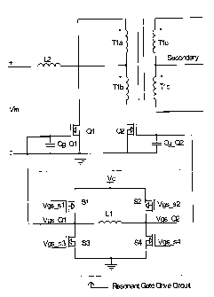
1 Dual low-side symmetrical resonant gate drive circuit
This section discusses in detail, with circuit topology, operation of the
resonant gate drive circuit for a dual low-side symmetrical MOSFET drive. For
example, it may be used to drive synchronous rectifiers in a current
13
CA 02594945 2007-07-16
WO 2006/079219
PCT/CA2006/000117
doubler configuration (e.g., Figure 5). It may also be used to drive the
primary
MOSFET in both current fed push-pull converters (e.g., Figure 6) and voltage-
fed
push pull converters (e.g., Figure 7). The circuit may also be used in other
power
converters as will be evident to one skilled in the art.
1.1 Topology
A resonant gate drive circuit for dual low-side symmetrical MOSFET drive is
shown in Figure 4. The circuit consists of four switches, S1 - S4, connected
in a
bridge (e.g., full bridge) configuration, and one inductor, Ll, connected
across the
bridge. Gate capacitances, Cg_Q1 and Cg_Q2, are the load of the resonant gate
drive circuit. Vc is the voltage source. To simplify the implementation, P-
channel
MOSFETs are used for S1 and S2, and N-channel MOSFETs are used for S3 and
S4. It is noted that other implementation methods may also be used to achieve
same objective. Other suitable devices for switches S1 - S4 include, for
example,
BJTs (bipolar junction transistors), IGBTs, and diodes.
The resonant gate drive circuit shown in Figure 4 charges and discharges
gate capacitances Cg_Q1 and Cg_Q2 with minimum energy loss and as quickly as
possible. When the capacitor voltage is high, the MOSFET is turned on and when
the capacitor voltage is low, the MOSFET is turned off. With this circuit, the
duty
cycles of the voltages across Cg_Q1 and Cg_Q2 are same. The duty cycle may
be higher than 0.5, equal to 0.5, or lower than 0.5. The actual duty cycle
will be
decided by the gate drive signals for S1 ¨ S4. The duty cycle D is defined as
the
ratio between the time when the MOSFET is on and the switching period, or D =
Ton / Ts, where Ton is the MOSFET on time and Ts is switching period.
Figure 5 shows the circuit when the dual low-side symmetrical resonant gate
drive circuit is used to drive the synchronous rectifiers of a current doubler
circuit.
14
CA 02594945 2007-07-16
WO 2006/079219
PCT/CA2006/000117
In the circuit, Q1 and Q2 are MOSFETs used as a synchronous rectifier. Cg_Q1
and Cg_Q2 represent the gate capacitances of MOSFET Q1 and Q2, respectively.
In this circuit, the duty cycles for Q1 and Q2 are same and the duty cycle is
larger
than 50%.
With the resonant gate drive circuit, the energy stored in the gate of Q1 and
Q2 is recovered. In addition, the turn on and turn off time of Q1 and Q2 are
also
reduced, which reduces their conduction loss.
The resonant gate drive circuit may also be used in other switching power
converters. Figure 6 shows a current fed push-pull converter with a resonant
gate
drive circuit to drive the primary side MOSFETs, Q1 and Q2. In this converter,
the
duty cycle for Q1 and Q2 is same and is larger than 50%.
The resonant gate drive circuit shown in Figure 4 may also be used for power
converters when the duty cycle is less than 0.5. Figure 7 shows a voltage fed
push-pull converter with a resonant gate drive circuit. In this converter, the
duty
cycle for Q1 and Q2 is the same and is less than 0.5.
With different gate drive signals to S1, S2, S3, and S4, the duty cycle for Q1
and Q2 may be changed from below 0.5, to 0.5 and to above 0.5. The following
sections describe the operation of the resonant gate drive circuit, as shown
in
Figure 4, under different duty cycle conditions.
1.2 Operation for D > 0.5
When the duty cycle is larger than 0.5, the operation of the dual low-side
symmetrical resonant gate drive circuit, as shown in Figure 4, can be analyzed
by
the key waveforms shown in Figure 8. In the figure, Vsg_S1, Vsg_S2, Vgs_S3,
and Vgs_S4 are gate drive signals for S1 - S4. Vgs_Q1 and Vgs_Q2 are the
voltage across Cg_Q1 and Cg_Q2. The rising edge and falling edge of
CA 02594945 2007-07-16
WO 2006/079219
PCT/CA2006/000117
Vgs_Q1 and Vgs_Q2 are shown to illustrate the details of the charging and
discharging interval. IL1 is the current waveform through inductor L1.
The following describes in detail the operation of the dual low-side
symmetrical resonant gate drive circuit for D > 0.5. Refer to the key
waveforms in
Figure 8 and circuit in Figure 4.
= Before tO:
S1 , S4 are on and S2, S3 are off. Q1 is on and Q2 is off. Inductor current
IL1
increases to maximum value at to.
= From tO to tl:
S4 is turned off at to. Inductor L1 resonates with the gate capacitor of
MOSFET Q2, Cg_Q2. Cg_Q2 is charged during this period. The voltage across
Cg_Q2 increases and it is clamped to the source voltage Vc by the body diode
of
S2 before t1. Q2 is turned on in this time interval. At t1, S2 turns on with
zero
voltage. By controlling the turn-off instant for S4 (t0), the turn-on instant
of Q2 can
be controlled.
= From t1 to t2:
S1, S2 are on and S3, S4 are off. Both Q1 and Q2 are on and inductor
current IL1 is circulating through S1 and S2 and remains constant in this
interval.
= From t2 to t3:
S1 is turned off at t2 with zero voltage. Inductor L1 resonates with the gate
capacitor of MOSFET Q1, Cg_Q1. Cg_Q1 is discharged during this period. The
voltage across Cg_Q1 decreases and it is clamped to zero by the body diode of
S3
before t3. Q1 is turned off in this time interval. At t3, S3 turns on with
zero voltage.
16
CA 02594945 2007-07-16
WO 2006/079219
PCT/CA2006/000117
By controlling the turn-off instant of S1 (t2), the turn-off instant of Q1 can
be
controlled.
= From t3 to t4:
S2, S3 are on and S1, S4 are off. Q1 is off and Q2 is on. The inductor
current IL1 decreases to zero and then it increases in the opposite direction.
It
reaches the negative maximum at t4.
= From t4 to t5:
S3 is turned off at t4. Inductor L1 resonates with capacitor Cg_Q1. Cg_Q1 is
charged during this interval. The voltage across Cg_Q1 increases and it is
clamped to the source voltage Vc by the body diode of S1 before t5. Q1 is
turned
on in this time interval. At t5, S1 turns on with zero voltage. By controlling
the turn
off instant of S3 (t4), the turn-on instant of Q1 can be controlled.
= From t5 to t6:
S1 , S2 are on and S3, S4 are off. Both Q1 and Q2 are on and inductor current
IL1 circulates through S1 and S2 and remains constant in this interval.
= From t6 to t7:
S2 is turned off at t6 with zero voltage. Inductor L1 resonates with capacitor
Cg_Q2. Cg_Q2 is discharged during this period. The voltage across Cg_Q2
decreases and it is clamped to zero by the body diode of S4 before t7. Q2 is
turned off in this time interval. At t7, S4 turns on with zero voltage. By
controlling
the turn off instant for S2 (t6), the turn-off instant of Q2 can be
controlled.
= From t7 to 69:
Sl, S4 are on and S2, S3 are off. Q1 is on and Q2 is off. The negative
17
CA 02594945 2007-07-16
WO 2006/079219
PCT/CA2006/000117
inductor current rises through zero and then further increases. The value of
the
current IL1 increases to positive maximum at t8. The next cycle starts at t8.
1.3 Operation for D = 0.5
When the duty cycle equals 0.5, the operation of the dual low-side
symmetrical resonant gate drive circuit, as shown in Figure 4 and Figure 5,
can be
analyzed by the key waveforms shown in Figure 9. The operation is similar to
that
for D > 0.5 (see above). In the figure, Vsg_S1, Vsg_S2, Vgs_S3, and Vgs_S4 are
gate drive signals for S1 ¨ S4. Vgs_Q1 and Vgs_Q2 are the voltages across
Cg_Q1 and Cg_Q2. The rising edge and falling edge of Vgs_Q1 and Vgs_Q2 are
shown to illustrate the details of the charging and discharging interval. ILI
is the
current waveform through inductor L1.
1.4 Operation for D < 0.5
When the duty cycle is less than 0.5, the operation of the dual low-side
symmetrical resonant gate drive circuit, as shown in Figure 4 and Figure 5,
can be
analyzed by key waveforms shown in Figure 10. The operation is similar to that
for
D > 0.5 (see above). In the figure, Vsg_S1, Vsg_S2, Vgs_53, and Vgs_S4 are
gate drive signals for S1 ¨ S4. Vgs_Q1 and Vgs_Q2 are the voltages across
Cg_Q1 and Cg_Q2. The rising edge and falling edge of Vgs_Q1 and Vgs_Q2 are
shown to illustrate the details of the charging and discharging interval. ILI
is the
current waveform through inductor L1.
2 Dual low-side complementary resonant gate drive circuit
This section discusses in detail the circuit topology and operation of a
resonant gate drive circuit for a dual low-side complementary MOSFET drive.
For
example, the circuit may be used to drive the synchronous rectifiers for a
forward
18
CA 02594945 2007-07-16
WO 2006/079219
PCT/CA2006/000117
converter. The circuit may also be used for other power converters as will be
evident to one skilled in the art.
2.1 Topology
,
The resonant gate drive circuit for dual low-side complementary MOSFET
drive is shown in Figure 11. Similar to the dual low-side symmetrical resonant
gate
drive circuit shown in Figure 4, the circuit consists of four switches, S1 ¨
S4,
connected in a bridge configuration, and one inductor, L1, connected across
the
bridge. Capacitor C1 is in series with the inductor L1. This capacitor is used
to
block the DC current flowing through the inductor L1. Gate capacitors Cg_Q1
and
Cg_Q2 are the load of the resonant gate drive circuit. Vc is the voltage
source.
The circuit shown in Figure 11 charges and discharges gate capacitances ,
Cg_Q1 and Cg_Q2 with minimum energy loss and as quickly as possible. With
this circuit, the duty cycles of the voltage across Cg_Q1 and Cg_Q2 are
complementary. That is, if the duty cycle for the voltage across Cg_Q1 is D,
then
the duty cycle for the voltage across Cg_Q2 is 1 ¨ D. In order to simplify the
implementation, P-channel MOSFETs are used for S1 and S2 and N-channel
MOSFETs are used for S3 and S4. It is noted that other implementations may
also
be used to achieve the same effect.
Figure 12 shows the circuit when the dual low-side complementary resonant
gate drive circuit is used to drive the synchronous rectifiers of a forward
converter.
In the circuit, Q1 and Q2 are MOSFETs used as a synchronous rectifier. Cg_Q1
and Cg_Q2 represent the gate capacitances of MOSFETs Q1 and Q2,
respectively. In the circuit, the duty cycle for Q1 is D and the duty cycle
for Q2 is 1
¨D.
With the resonant gate drive circuit, the energy stored in the gate of Q1 and
19
CA 02594945 2007-07-16
WO 2006/079219
PCT/CA2006/000117
Q2 is recovered by the resonant gate drive circuit. In addition, the turn-on
time and
turn-off time of Q1 and Q2 are reduced, which reduces their conduction loss.
2.2 Operation
The operation of the dual low-side complementary resonant gate drive circuit,
as shown in Figure 11, can be analyzed by the key waveforms shown in Figure
13.
In the figure, Vsg_S1, Vsg_S2, Vgs_S3, and Vgs_S4 are gate drive signals for
S1
¨ S4. Vgs_Q1 and Vgs_Q2 are the voltages across Cg_Q1 and Cg_Q2. The
rising edge and falling edge of Vgs_Q1 and Vgs_Q2 are shown to illustrate the
details of the charging and discharging intervals. IL1 is the current waveform
through inductor L1. In the analysis, it is assumed that capacitor C1 is very
large
and the voltage across Cl is a DC value. If the capacitor value C1 is small,
the
operation of the circuit does not change.
The following provides a detailed description of the operation of the dual low-
side complementary resonant gate driver circuit. The duty cycle for Q1 is D
and
the duty cycle for Q2 is 1 ¨ D. Refer to the key waveforms in Figure 13 and
the
circuit in Figure 12.
= Before tO:
S1 , S4 are on and 32, S3 are off. Q1 is on and Q2 is off. Inductor current
IL1
increases to the maximum value at to.
= From tO to tl:
S1 is turned off at tO. Inductor L1 resonates with the gate capacitor of
MOSFET Q1, Cg_Q1. Cg_Q1 is discharged during this period. The voltage
across Cg_Q1 decreases and it is clamped to zero by the body diode of S3
before
CA 02594945 2007-07-16
WO 2006/079219
PCT/CA2006/000117
t1 . Q1 is turned off in this time interval. At t1, S3 is turned on and S4 is
turned off
with zero voltage simultaneously. By controlling the turn-off instant for S1
(t0), the
turn-off instant of Q1 can be controlled.
= From ti to t2:
S3 is turned on and S4 is turned off with zero voltage at ti simultaneously.
Inductor L1 resonates with the gate capacitor of MOSFET Q2, Cg_Q2. Cg_Q2 is
charged during this period. The voltage across Cg_Q2 increases and it is
clamped
to the source voltage Vc by the body diode of S2 before t2. Q2 is turned on in
this
time interval. At t2, S2 is turned on with zero voltage. By controlling the
turn-on
instant for S3 (t1), the turn-on instant for Q2 can be controlled.
= From t2 to t3:
S1, S4 are off and S2, S3 are on. Q1 is off and Q2 is on. The inductor
current (Li decreases to zero and then it increases in the opposite direction.
It
reaches negative maximum at t3. At t3, 82 is turned off with zero voltage.
= From t3 to t4:
S2 is turned off at t3. Inductor L1 resonates with capacitor Cg_Q2. Cg_Q2 is
discharged during this period. The voltage across Cg_Q2 decreases and it is
clamped to zero by the body diode of S4 before t4. Q2 is turned off in this
time
interval. At t4, S3 is turned off and S4 is turned on with zero voltage
simultaneously. By controlling the turn-off instant for S2 (t3), the turn-off
instant of
Q2 can be controlled.
= From t4 to t5:
S3 is turned off and S4 is turned on with zero voltage at t4 simultaneously.
Inductor L1 resonates with capacitor Cg_Ql. Cg_Q1 is charged during this
period.
21
CA 02594945 2007-07-16
WO 2006/079219
PCT/CA2006/000117
The voltage across Cg_Q1 increases and it is clamped to the source voltage Vc
by
the body diode of S1 before t5. Q1 is turned on in this time interval. At t5,
Si is
turned on with zero voltage. By controlling the turn-off instant for S3 (t4),
the turn-
on instant for Q1 can be controlled.
= From t5 to t6:
S1, S4 are on and S2, S3 are off, while Q1 is on and Q2 is off. The negative
inductor current IL1 rises through zero and further increases. The value of
the
inductor current ILI increases to positive maximum at t6. The next cycle
starts at
t6.
3 Dual high-side and low-side resonant gate drive circuit
This section discusses in detail the circuit topology and operation of a
resonant gate drive circuit for dual low-side and high-side complementary or
symmetrical MOSFET drive. For example, the circuit may be used to drive the
control MOSFET and synchronous MOSFET of a buck converter. The circuit may
be used to drive the high-side and low-side MOSFET in a half-bridge converter
or a
full-bridge converter. It may also be used for phase shift in a full bridge
converter.
The circuit may also be used for other power converters as will be evident to
one
skilled in the art.
3.1 Topology
A resonant gate drive circuit for dual high-side and low-side complementary
MOSFET drive is shown in Figure 14. The circuit consists of four switches, S1
¨
S4, one inductor, Ll, two capacitors, Cl and C2, and one diode, Dl. Capacitor
C1
is used to block the DC current flow through inductor Ll. Capacitor C2 is a
flying
capacitor that is used for high-side drive. Diode DI is used to charge the
capacitor
22
CA 02594945 2007-07-16
WO 2006/079219
PCT/CA2006/000117
C2 to a voltage above the supply voltage Vc. Gate capacitors Cg_Q1 and Cg_Q2
are the load of the resonant gate drive. It is noted that one end of Cg_Q2 is
connected to ground. However, neither end of Cg_Q1 is connected to ground.
This capacitor is floating. This is required for high-side drive. To simplify
the
implementation, P-channel MOSFETs are used for Si and S2 and N-channel
MOSFETs are used for S3 and S4. It is noted that other implementations may
also
be used to achieve the same effect.
The resonant gate drive circuit shown in Figure 14 charges and discharges
the gate capacitors Cg_Q1 and Cg_Q2 with minimum energy loss and as quickly
as possible. When the gate capacitor voltage is high, the MOSFET is turned on,
and when the gate capacitor voltage is low, the MOSFET is turned off.
Figure 15 shows a dual high-side and low-side resonant gate drive circuit
used to drive the two MOSFETs in a buck converter. In the circuit, Q1 is the
control MOSFET and Q2 is the synchronous drive MOSFET. Cg_Q1 and Cg_Q2
are gate capacitors for Q1 and Q2, respectively. The duty cycle for Q1 is D
and
the duty cycle for Q2 is 1 ¨ D.
With the resonant gate drive circuit, the energy stored in the gate of Q1 and
Q2 is recovered. In addition, the turn-on and turn-off time of Q1 and Q2 are
reduced as compared with a conventional gate drive circuit. One benefit is
lower
switching loss for Q1 and lower conduction loss for Q2. The efficiency of the
buck
converter is therefore improved.
The dual high-side and low-side resonant gate drive circuit shown in Figure 14
may also be used in other circuit topologies. For example, Figure 16 shows an
asymmetrical half bridge converter with dual resonant gate drive circuits. At
the
primary side, a dual high-side and low-side complementary resonant gate drive
23
CA 02594945 2007-07-16
WO 2006/079219
PCT/CA2006/000117
circuit is used, and at the secondary side, a dual low-side complementary
resonant
gate drive circuit is used.
In Figure 15 and Figure 16, the dual high-side and low-side resonant gate
drive circuit generates a complementary gate signal. It generates D for Q1 and
1 ¨
D for Q2. The waveforms are shown in Figure 19. It is noted that this circuit
can
also generate a symmetrical duty cycle for Q1 and Q2. Figure 17 shows a half-
bridge converter with a dual high-side and low-side resonant gate drive
circuit.
In Figure 17, Cg_Q1 and Cg_Q2 represent the gate capacitors of MOSFETs
Q1 and Q2, respectively. The duty cycles for Q1 and Q2 are both D. The
waveforms are shown in Figure 20.
Figure 18 shows a full-bridge converter with dual high-side and low-side
symmetrical resonant gate drive circuits. In the circuit, two dual high-side
and low-
side resonant gate drive circuits are used, one for the left side and one for
the right
side. Cg_Q1, Cg_Q2, Cg_Q3, and Cg_Q4, not shown, are the gate capacitances
of Q1, Q2, Q3, and Q4, respectively.
3.2 Operation for complementary gate drive signal
The resonant gate drive circuit shown in Figure 14 may operate in both
complementary and symmetrical mode. Operation of the circuit in complementary
gate drive mode is discussed in this section and operation of the circuit in
symmetrical gate drive mode is discussed in section 3.3.
Operation of a dual high-side and low-side complementary resonant gate
drive circuit, as shown in Figure 14, can be analyzed by the key waveforms
shown
in Figure 19. In Figure 19, Vsg_S1, Vsg_S2, Vgs_S3, and Vgs_S4 are gate drive
signals for S1 ¨ S4. Vgs_Q1 and Vgs_Q2 are the voltages across Cg_Q1 and
Cg_Q2. The rising edge and falling edge of Vgs_Q1 and Vgs_Q2 are
24
CA 02594945 2007-07-16
WO 2006/079219
PCT/CA2006/000117
shown to illustrate the details of the charging and discharging intervals. IL1
is the
current waveform through inductor L1. In the analysis, it is assumed that
capacitor
C1 is very large and the voltage across Cl is a DC value. If the capacitor
value C1
is small, operation of the circuit does not change. The capacitor value for C2
is
very large and the voltage across C2 is a DC value.
The following provides a detailed description of the operation of a dual high-
side and low-side resonant gate driver circuit operating in complementary
mode.
The duty cycle for Q1 is D and duty cycle for Q2 is 1 ¨ D. Refer to the key
waveforms in Figure 19 and the circuit of Figure 14.
= Before tO:
Sl, S4 are off and S2, S3 are on. Q1 is off and Q2 is on. The inductor
current, IL1, increases to negative maximum value. The inductor current IL1
flows
in the loop consisting of S2, C1, L1, S3, Q2 and Vc. The voltage across C2 is
charged to the level of Vc via D1 and Q2.
= From tO to t 1:
S2 is turned off at to. Inductor L1 resonates with the gate capacitor of
MOSFET Q2, Cg_Q2. Cg_Q2 is discharged during this period. The voltage
across Cg_Q2 decreases and it is clamped to zero by the body diode of S4
before
t1. Q2 is turned off in this time interval. The current IL1 flows in the loop
consisting
of Cg_Q2, Cl, L1, 83 and Q2. Then at t1, S3 is turned off and 84 is turned on
with
zero voltage simultaneously. By controlling the turn-off instant for S2 (t0),
the turn-
off instant of Q2 can be controlled.
= From ti to t2:
S3 is turned off and S4 is turned on with zero voltage at t1 simultaneously.
CA 02594945 2007-07-16
WO 2006/079219
PCT/CA2006/000117
Inductor L1 resonates with the gate capacitor of MOSFET Q1, Cg_Q1. Cg_Q1 is
charged during this period. The voltage across Cg_Q1 increases and it is
clamped
to the level of Vc by the body diode of S1 before t2. Q1 is turned on in this
time
interval. The current ILI flows in the loop consisting of S4, C1, L1, Cg_Q1,
Q1,
and Vc after Q1 is turned on. Then at t2, S1 is turned on with zero voltage.
By
controlling the turn-off instant for S3 (t1), the turn-on instant for Q1 can
be
controlled.
= From t2 to t3:
S1, S4 are on and 52, S3 are off. Q1 is on and Q2 is off. The negative
inductor current IL1 rises to zero and further increases. The value of the
current
IL1 increases to positive maximum at t3. The current IL1 flows in the loop
consising of C2, S1, L1, C1, 84, Vc, and Q1. Then at t3, S1 is turned off with
zero
voltage.
= From t3 to t4:
S1 is turned off at t3. Inductor L1 resonates with capacitor Cg_Q1. Cg_Q1 is
discharged during this period. The voltage across Cg_Q1 decreases and it is
clamped to zero by the body diode of S3 before t4. Q1 is turned off in this
time
interval. The current IL1 flows in the loop consisting of Cg_Q1, L1, C1, 84,
Vc, and
Q1. At t4, S3 is turned on and S4 is turned off with zero voltage
simultaneously.
By controlling the turn-off instant for S1 (t3), the turn-off instant of Q1
can be
controlled.
= From t4 to t5:
S3 is turned on and S4 is turned off with zero voltage at t4 simultaneously.
Inductor Ll resonates with capacitor Cg_Q2. Cg_Q2 is charged during this
period.
The voltage across Cg_Q2 increases and it is clamped to the
26
CA 02594945 2007-07-16
WO 2006/079219
PCT/CA2006/000117
source voltage Vc by the body diode of S2 before t5. Q2 is turned on in this
time
interval. The current IL1 flows in the loop consisting of S3, Ll , C1, Cg_Q2,
and
Q2. At t5, S2 is turned on with zero voltage. By controlling the turn-on
instant for
S3 (t4), the turn-on instant for Q2 can be controlled.
= From t5 to t6:
S1 , S4 are off and S2, S3 are on, while Q1 is off and Q2 is on. The inductor
current IL1 decreases to zero and then it increases in the opposite direction.
The
value of the current ILI increases to negative maximum at t6. The current 11
flows in the loop consisting of 82, C1, L1, S3, Q2 and Vc. The next cycle
starts at
t6.
3.3 Operation for symmetrical gate drive signal
As discussed earlier, the dual high-side and low-side resonant gate drive
circuit shown in Figure 14 may also operate in symmetrical duty cycle mode.
Converters such as half bridge converters and full bridge converters require
this
operation mode.
The symmetrical signal operation can be analyzed by the key waveforms
shown in Figure 20. In the figure, Vsg_S1, Vsg_S2, Vgs_S3, and Vgs_S4 are gate
drive signals for S1 ¨ S4. Vgs_Q1 and Vgs_Q2 are the voltages across Cg_Q1
and Cg_Q2. The rising edge and falling edge of Vgs_Q1 and Vgs_Q2 are shown
to illustrate the details of the charging and discharging intervals. ILI is
the current
waveform through inductor L1. In the analysis, it is assumed that capacitor C1
is
very large and the voltage across C1 is a DC value. If the capacitor value C1
is
small, the operation of the circuit does not change. The capacitor value for
C2 is
very large and the voltage across C2 is a DC value.
The following provides a detailed
description of the operation of a
27
CA 02594945 2007-07-16
WO 2006/079219
PCT/CA2006/000117
dual high-side and low-side resonant gate driver circuit operating at
symmetrical
mode. The duty cycles for Q1 and Q2 are both D, with half switching period
shift
between each other. Refer to the key waveforms in Figure 20 and the circuit in
Figure 14.
= Before tO:
S2, S3 are on and S1, 84 are off. Q1 is off and Q2 is on. The inductor
current reaches negative maximum at to. The inductor current, ILA, flows
through
S2, C1, L1, S3, Q2, and Vc. The voltage across C2 is charged to the level of
Vc
via D1 and Q2.
= From tO to tl:
S2 is turned off at tO with zero voltage. Inductor L1 resonates with the gate
capacitor of Q2, Cg_Q2. Cg_Q2 is discharged during this period. The voltage
across Cg_Q2 decreases and it is clamped to zero by the body diode of S4
before
t1. Q2 is turned off in this time interval. The current IL1 flows through
Cg_Q2, C1,
L1, S3, and Q2. At t1, S4 is turned on with zero voltage. By controlling the
turn-off
instant for S2 (t0), the turn-off instant for Q2 can be controlled.
= From ti to t2:
S3, S4 are on and S1, S2 are off. Both Q1 and Q2 are off. The inductor
current IL1 remains constant in this interval. The current ILA flows through
S4, Cl,
L1, S3, the primary winding of the transformer, C3, C4, and Vc.
= From t2 to t3:
S3 is turned off at t2 with zero voltage. Inductor L1 resonates with the gate
capacitor of Q1, Cg_Q1. Cg_Q1 is charged during this period. The voltage
across
Cg_Q1 increases and it is clamped to the level of Vc by the body diode of S1
28
CA 02594945 2007-07-16
WO 2006/079219
PCT/CA2006/000117
before t3. Q1 is turned on in this time interval. The current IL1 flows
through S4,
C1, L1, Cg_Q1, Q1, and Vc after Q1 is turned on. At t3, S1 is turned on with
zero
voltage. By controlling the turn-off instant for S3 (t2), the turn-on instant
for Q1 can
be controlled.
= From t3 to t4:
S1, S4 are on and S2, S3 are off. Q1 is on and Q2 is off. The inductor
current increases from the negative maximum, through zero and reaches a
positive
maximum at t4. The current IL1 flows through S4, Cl, L1, S1, C2, Q1, and Vc.
= From t4 to t5:
S1 is turned off at t4 with zero voltage. Inductor L1 resonates with Cg_Q1.
Cg_Q1 is discharged during this period. The voltage across Cg_Q1 decreases and
it is clamped to zero by the body diode of S3 before t5. Q1 is turned off in
this time
interval. The current IL1 flows through Cg_Q1, L1, Cl, S4, the primary winding
of
the transformer, C3, C4, and Vc after Q1 is turned off. At t5, S3 is turned on
with
zero voltage. By controlling the turn-off instant for S1 (t4), the turn-off
instant of Q1
can be controlled.
= From t5 to t6:
S3, S4 are on and S1, S2 are off. Both Q1 and Q2 are off. The inductor
current IL1 is constant in this interval. The current 11 flows through S3, L1,
C1,
S4, Vc, C3, C4, and the primary winding of the transformer.
= From t6 to t7:
S4 is turned off at t6 with zero voltage. Inductor L1 resonates with Cg_Q2.
Cg_Q2 is charged during this period. The voltage across Cg_Q2 increases and it
is clamped to the source voltage Vc by the body diode of S2 before t7. Q2 is
29
CA 02594945 2007-07-16
WO 2006/079219
PCT/CA2006/000117
turned on in this time interval. The current IL1 flows through S3, L1, C1,
Cg_Q2,
and Q2 after Q2 is turned on. Then at t7, S2 is turned on with zero voltage.
By
controlling the turn-off instant for S4 (t6), the turn-on instant of Q2 can be
controlled.
= From t7 to t8:
S2, S3 are on and S1, S4 are off. Q1 is off and Q2 is on. The inductor
current IL1 decreases to zero and it increases to a negative maximum at t8.
The
current IL1 flows through S2, Cl, L1, S3, Q2, and Vc. The next cycle starts at
t8.
4. Single High-side or Low-side Resonant Gate Drive Circuit
This section discusses in detail the circuit topology and operation of a
resonant gate drive circuit for single high-side or low-side MOSFET gate
drive, such
as that shown in the general block diagram of Figure 1 The circuit achieves
quick
turn-on and turn-off transition times to reduce switching loss and conduction
loss in
power MOSFETS using turn-on and turn-off pre-charge intervals. The driver
returns
energy to the line during intervals after the MOSFET is turned-on and after it
is
turned-off. The circuit may be used to drive, for example, the control MOSFET
or the
synchronous MOSFET of a buck converter. The circuit may be used to drive the
high-side or the low-side MOSFET in a half bridge converter or a full bridge
converter. It may also be used for phase shift in a full bridge converter. The
circuit
may also be used for other power converters as will be evident to one skilled
in the
art.
4.1 Topology
Referring to Figure 21, the circuit consists of four control switches S1 - S4
and
a small resonant inductance L. BD1 to BD4 are the body diodes of switches S1 -
CA 02594945 2007-07-16
WO 2006/079219
PCT/CA2006/000117
S4. The power switch Q is the switch to be driven. The gate capacitance of the
power switch Q is not shown. The current iL through the resonant inductance L
is
discontinuous to minimize circulating current conduction loss. The four
control
switches switch with near zero switching loss. The switches S1, S3 closest to
the
power switch Q turn on with zero voltage switching and turn off in a lossless
manner since they are shunted by the power switch gate capacitance. The
switches S2, S4 farthest from the power switch Q have both zero voltage and
zero
current transitions. The peak inductor current and gate current are
controlled, so
they are independent of duty cycle, or switching frequency. P-channel MOSFETs
are shown for control switches S1 and S2 due to the simple driving
requirements;
however they may be replaced by N-channel MOSFETs. In such case their gating
waveforms would be complementary.
4.2 Operation
Operation of the circuit shown in Figure 21 will now be explained with
reference to the waveforms shown in Figure 22(a). In order from top to bottom,
the
waveforms represent: 1) the control switch S1 gating waveform, 2) the control
switch S2 gating waveform, 3) the control switch S3 gating waveform, 4) the
control
switch 84 gating waveform, 5) the inductor current, 6) the power MOSFET gate
current, 7) the power MOSFET gate-to-source driving voltage, and 7) the line
current from the control voltage source.
The power MOSFET gate terminal is modeled as a capacitance, Cg. Initially
it is assumed that the power MOSFET is in the off state before time to. For
the
control switches, the shaded regions in Figure 22(a) indicate the on-state, so
initially only switches S3 and S4 are on and the gate of Q is clamped to zero
volts.
In all cases, a small dead-time (not shown) is added between the complementary
transitions of S2 and S4 to eliminate shoot-through and allow zero voltage
31
CA 02594945 2007-07-16
WO 2006/079219
PCT/CA2006/000117
switching (ZVS) or zero current switching (ZCS).
From tO to ti
Initially, before time to, S3 and S4 are on, the inductor current is zero, and
the
power MOSFET gate is clamped low. At time tO, S4 turns off (with ZCS) and then
S2 turns on (with ZCS) allowing the inductor current to ramp up. The current
path
during this interval is S2-L-S3. Since S3 is in the on state, the gate of Q is
clamped
low. The interval ends at time t1.
From ti to t2:
At time t1, S3 turns off (with approximate ZVS due to large shunt power
MOSFET gate capacitance), which allows the inductor current to begin to charge
the power MOSFET gate. Since the dotted side of the inductor is clamped to the
line and the other side is connected to the gate capacitance of Q, the
inductor
current continues to ramp up, but with a reduced slope as the voltage across
the
gate capacitance increases. The current path during this interval is S2-L-Cg.
This
interval ends at time t2, when Vgs reaches Vcc. If this interval is allowed to
continue, the body diode BD1 of switch S1 allows the current to freewheel
through
S2-L-BD1.
From t2 to t3:
At time t2, S2 turns off and S1 and then S4 turn on (both with ZVS), allowing
the inductor current to conduct into the dot through the path S4-L-S1.
Importantly,
it is during this interval that the gate charging energy is returned to the
line. This
can be observed from the negative portion of the iVcc curve in Figure 22(a).
Also,
during this interval, the inductor voltage becomes reverse biased, so the
inductor
current quickly ramps down towards zero. During this interval, the gate
voltage of
32
CA 02594945 2007-07-16
WO 2006/079219
PCT/CA2006/000117
Q remains clamped to the line voltage, Vcc. The interval ends when the
inductor
current reaches zero at time t3.
From t3 to t4:
At time t3, S4 turns off (with ZCS) and then S2 turns on (with ZCS), which
allows any residual inductor current to freewheel through S2-L-S1. During this
interval, the gate voltage of Q remains clamped to Vcc. The interval ends at
time
t4 when the pre-charging interval for the turn-off cycle begins as dictated by
the
PWM signal from the controller.
From t4 to t5:
At time t4, the turn-off pre-charging interval begins. S2 turns off (with ZCS)
and S4 turns on (with ZCS). Since S1 was previously on, the inductor current
begins to ramp negative out of the dot through the path Sl-L-S4. During this
interval, the gate voltage of Q remains clamped to Vcc. The interval ends at
time
t5.
From t5 to t6:
At time t5, S1 turns off (with shunted ZVS from Q), which allows the inductor
current to begin to discharge the power MOSFET gate. Since the dotted side of
the inductor is clamped to ground and the other side is connected to the gate
capacitance of Q, the inductor current continues to ramp negative, but with a
reduced slope as the voltage across the gate capacitance decreases. The
current
path during this interval is Cg-L-S4. This interval ends at time t6, when Vgs
reaches zero. If this interval is allowed to continue, the body diode of
switch S3 will
allow the current to freewheel through BD3-L-S4.
33
CA 02594945 2007-07-16
WO 2006/079219
PCT/CA2006/000117
From t6 to t7:
At time t6, S4 turns off and S2 and S3 turn on (both with ZVS), allowing the
inductor current to conduct out of the dot through the path S3-L-S2.
Importantly, it
is also during this interval that the gate discharging energy is returned to
the line.
This can be observed from the negative portion of the iVcc curve in Figure
22(a).
Also, during this interval, the inductor voltage has become reverse biased, so
the
inductor current quickly ramps down positive towards zero. During this
interval, the
gate voltage of Q remains clamped to ground. The interval ends when the
inductor
current reaches zero at time t7.
From t7 to tO:
At time t7, S2 turns off (with ZCS) and S4 turns on (with ZCS), which allows
any residual inductor current to freewheel through S3-L-S4. During this
interval,
the gate voltage of Q remains clamped to ground. The interval ends at time tO
when the pre-charging interval for the turn-on cycle begins and the entire
process
repeats as dictated by the PWM signal from the controller.
It can be observed from the operating intervals and the line current iVcc that
energy is taken from the line voltage Vcc during three intervals, tO - ti, t1 -
t2 and
t4 - t5 and energy is returned to the line during two intervals, t2 - t3 and
t6 - t7.
4.3 Reduced Pulse Embodiments
From Figure 22(a) it can be seen that the gating signals for control switches
S2 and S4 contain three pulses per switching period. In addition, the current
through the control switches during the intervals labelled 2 (t3 - t4), 3 (t6 -
t7), 5 (t7
- tO) and 6 (t2 - t3) is in the same direction as the body diode. In these
cases, it is
not required that the control switches be turned on. If left off, gate loss in
the
34
CA 02594945 2007-07-16
WO 2006/079219
PCT/CA2006/000117
control switches can be saved.
There are two pulses for S2 and two for S4 that can be eliminated by using
the body diodes, which provides three alternative embodiments of this resonant
gate driver. The pulses that can be eliminated by using the body diodes, or
external diodes, are labelled 2 and 3 for 82, and 5 and 6 for S4.
Reduced Pulse Embodiment 1 (2-pulse)
If pulse 2 is eliminated from S2 and pulse 5 is eliminated from S4 in Figure
22(a), energy can be saved for these switches in the form of gate loss and
output
loss (CV2) at turn-on. The body diodes (or external diodes) can be used to
clamp
the voltage across the inductor, allowing negligible current to circulate in
the driver.
In this case during the clamping interval t3 - t4, switch S1 is on along with
the body
diode of S2. During the other clamping interval 17 - tO, switch S3 is on along
with
the body diode of S4. Waveforms of this embodiment are shown in Figure 22(b).
Reduced Pulse Embodiment 2 (2-pulse)
If pulse 3 is eliminated from S2 and pulse 6 is eliminated from S4 in Figure
22(a), energy can be saved for these switches in the form of gate loss. The
body
diodes (or external diodes) can be used to provide the current paths when the
energy is returned to the line. In this case during the energy return interval
t2 - t3,
switch S1 is on along with the body diode of S4. During the other energy
return
interval t6 - t7, switch S3 is on along with the body diode of S2. Waveforms
of this
embodiment are shown in Figure 22(c)
Reduced Pulse Embodiment 3 (1-pulse)
The above two alternative embodiments may be combined by eliminating
pulses 2 and 3 from S2, and pulses 5 and 6 from S4, in Figure 22(a). Waveforms
CA 02594945 2007-07-16
WO 2006/079219
PCT/CA2006/000117
of this embodiment are shown in Figure 22(d).
4.4 High-side Drive Implementation
This resonant gate driver may be adapted for high-side drive of non-ground
referenced MOSFET switches using a bootstrap circuit consisting of a diode,
Db,
and capacitor, Cb, as illustrated in Figure 23. The equivalent gate
capacitance of
the power switch Q is not shown.
4.5 Dual High-side and Low-side Drive Implementation
The high-side driver shown in Figure 23 may be utilized along with the low-
side driver of Figure 21 to drive both switches in a bridge-leg configuration,
such
as, for example, a synchronous buck converter, a full-bridge converter, a half-
bridge converter, an active clamp forward converter, or a resonant converter
with a
full-bridge or half-bridge inverter. An example of such a circuit for driving
a bridge
leg is shown in Figure 24(a), where the equivalent gate capacitances of the
power
switches Q1 and Q2 are not shown. The bridge leg may be, for example, that of
a
synchronous buck converter, as shown in Figure 24(b). When implemented in a
bridge-leg configuration, the gate driver allows independent control of the
switching
speed of the two switches of the buck converter.
Exemplary waveforms for the circuit of Figure 24(b) to drive a synchronous
buck converter are shown in Figure 24(c). The input signals are the PWM signal
for the power switch Q1, labelled PWM1, and its complement PWM2 for Q2, with a
small dead time between PWM1 and PWM2. The eight control switch gating
signals are labelled S1 ¨ S8. The current waveforms for the two inductors L1
an
L2 are labelled iL1 and iL2. The gate-to-source voltage for MOSFET Q1 is
labelled
Vgs1 and the gate-to-source voltage for the synchronous rectifier MOSFET Q2 is
labelled Vgs2.
36
CA 02594945 2007-07-16
WO 2006/079219
PCT/CA2006/000117
4.6 Control Logic Example
An embodiment of the logic required to produce gating signals for the four
control switches S1 - S4 will now be described. The first point to be noted
from
Figure 22(a) is that S2 and S4 operate complementarily. However, since a P-
channel switch is used for S2, the same logic may be used to generate the
gating
signals for both switches, which simplifies the logic design and reduces the
gate
count requirement.
Logic waveforms used to create the three control signals for S1 - S4 of Figure
22(a) are showed in Figure 25(a). The only logic input to the gate drive
circuit is a
PWM signal generated by a converter controller. To implement appropriate pre-
charging intervals, gate charging intervals, and energy return intervals,
delay
circuitry is required to delay the PWM signal for the appropriate times. The
delayed signals are labeled D1 - D3 in Figure 25(a). The required gating
signals
for S1 - S4 are shown after the PWM signal and these signals were created
using
the logic circuit shown in Figure 26(a).
Control Logic for Reduced Pulse Embodiment '1 (2-pulse)
The logic waveforms used to create the four control signals for S1 ¨ S4
(Figure 22(b)) of reduced pulse embodiment 1 are shown in Figure 25(b). The
required gating signals for S1 - S4 are shown after the PWM signal and these
signals were created using the logic circuit shown in Figure 26(b).
Control Logic for Reduced Pulse Embodiment 2 (2-pulse)
The logic waveforms used to create the four control signals for S1 - S4
(Figure 22(c)) of reduced pulse embodiment 2 are shown in Figure 25(c). The
required gating signals for S1 - S4 are shown after the PWM signal and these
37
CA 02594945 2007-07-16
WO 2006/079219
PCT/CA2006/000117
signals were created using the logic circuit shown in Figure 26(c).
Control Logic for Reduced Pulse Embodiment 3 (1-pulse)
The logic waveforms used to create the four control signals for S1 - S4
(Figure 22(d)) of reduced pulse embodiment 3 are shown in Figure 25(d). The
required gating signals for S1 - S4 are shown after the PWM signal and these
signals were created using the logic circuit shown in Figure 26(d).
4.7 Design Example and Simulation Results
An isolated switching power converter, such as that shown in Figure 15, was
designed to operate at 1.5 MHz to deliver power to a 35 A load at 1 V. Two
pairs
of synchronous rectifier (SR) power MOSFETs were used in the secondary side
rectifier stage. The peak reverse voltage on the SRs was 4 V and their gates
were
driven by a 5 V source. The power MOSFET Q and control switches S1 - S4 were
selected and their relevant parameters are given in Table I. The turn on
transition
time was selected to be 10% of the switching period, corresponding to F = 0.1.
Table 1. Switch parameters for the resonant gate driver.
# Req RDS@ QG @ Qg @
Label Per Part # Vgs=4.5V V0s=4V V0s=5V
Driver [CA [nCl rnC] Min
2 IRF6691 NA
2(40)=80 NA 0.6/2=0.3
(Qg) (RG)
S1 1 FDN342P 0.062 (R1) NA 3.15
NA
1.35
S2 0.160(R2)
1 Si3585DV NA (QG2) NA
1.05
S4 0.100(R4)
('(G4
S3 1 FDN335N 0.055 (R3) NA 1.75
NA
Additional circuit parameters used to calculate the optimal inductance value
and conduction loss are summarized in Table 2.
38
CA 02594945 2007-07-16
WO 2006/079219
PCT/CA2006/000117
Table 2. Additional circuit parameters for the resonant gate drive circuit.
Label Value
Vcc 5V
F 0.1
fs 1.5 MHz
RL 0.05 D
Ra R2+ RL+R3=0.265 O
Rb R2+ RL+Rg=0.51 0
Re R4+RL+R/=0.212 O
Using the parameters in Tables 1 and 2 along with equation (1), the optimal
inductance value was calculated to be L= 170 nH. The required transition times
were calculated to be ta = 24 ns using equation (2), 1. t = 67 ns using
equation
.b = -on
(3), and tc= 58 ns using equation (4), corresponding to required delay times
of tdi =
24 ns, td2 = 90 ns, and td3 = 149 ns for the PWM signal.
Vcc, ({ _______________________________________________________
F 2 (Ra + 10213 + (4Rb + Re ¨ Ra +2V¨ RaRa + 4Rb2 +2RbRc ¨2RbRa)2/3
Qg 2fS j (Ra + 10113 (4Rb +Re ¨Ra +2A1¨ RcRa + 4Rb2 + 2RbRc ¨ 2RbRa)113
(1)
t a = LE[Q,fs Vcc F 11 (2)
vcc F 4 fs L
ton =Tr--F
(3)
J s
t
L [CV's Vcc, F 11
= (4)
C Vcc F 4 fs L
i ¨3 r 2 i 2 \
pond=2 Ls, It L [Ws Vcc F 1 +F] ft , 1.2,fsL 1 vc,/ ifs4 L [Qgfs iVcc F 11 (5)
f3 Vcc F 4 L_ F J\ 3 Vcc F 4 A L
i
PgQ2Q4 = 3fS(Qg2+Qg4)VCC (6)
39
CA 02594945 2013-12-12
Pgate QgVCC fS (7)
The total conduction loss in the driver was 194 mW, calculated using equation
(5). The additional gate loss attributed to S2 and S4 was 54 mW, calculated
using
equation (6). Since two drive circuits are required for the converter because
there
are two pairs of SRs, the total conduction loss and additional gate loss
quantities
were doubled and were 388 mW and 108 mW, respectively. The total loss using
the method described herein was 496 mW. The total gate loss using a
conventional gate driver was 1.2 W, calculated using equation (7) with four
IRF6691 SRs in the rectifier. Therefore, if the core loss of the inductors is
neglected, the efficiency of the gate driver of this embodiment was 59%. The
total
power savings was 704 mW for the given application, which represents 2% of the
total load power, which is significant given the high operating efficiencies
of present
day converters.
PSIM 5.0 was used to simulate the resonant gate driver, using the parameters
given above. The simulation waveforms are shown in Figure 27. The waveforms
from the top down are: 1) the PWM signal, 2) the Si and S3 gate waveforms, 3)
the S2 and S4 gate waveforms which overlap, 4) the inductor current waveform,
5)
the power MOSFET Q gate-to-source voltage approximating the gate as a series
resistance and capacitance, and 6) the line current. The average line current
was
measured to be 39 mA, which represents a total conduction loss in the circuit
of
195 mW, which agrees with the value of 194 mW calculated above.