Note: Descriptions are shown in the official language in which they were submitted.
CA 02594949 2013-07-22
OMNIDIRECTIONAL TILT AND VIBRATION SENSOR
CROSS-REFERENCE TO RELATED APPLICATIONS
The present application is a PCT Patent Application claiming priority to the
copending continuation application having the title "OMNIDIECTEONAL TILT AND
VIBRATION SENSOR," filed on January 13, 2006. The present application also
claims
priority to copending U.S. Patent Application Serial No. 11/037,497, filed
January 18, 2005,
and having the title "OMNIDIECTIONAL TILT AND VIBRATION SENSOR".
FIELD OF THE INVENTION
The present invention is generally related to sensors, and more particularly
is related to
an omnidirectional tilt and vibration censor.
BACKGROUND OF THE INVENTION
Many different electrical tilt and vibration switches are presently available
and known
to those having ordinary skill in the art. Typically, tilt switches are used
to switch electrical
circuits ON and OFF depending on an angle of inclination of the tilt switch.
These types of
tilt switches typically contain a free moving conductive element located
within the switch,
where the conductive element contacts two terminals when the conductive
element is moved
into a specific position, thereby completing a conductive path. An example of
this type of tilt
switch is a mercury switch. Unfortunately, it has been proven that use of
Mercury may lead
to
1
CA 02594949 2007-07-16
WO 2006/078602
PCT/US2006/001503
environmental concerns, thereby leading to regulation on Mercury use and
increased cost of
Mercury containing products, including switches.
To replace Mercury switches, newer switches use a conductive element capable
of
moving freely within a confined area. A popularly used conductive element is a
single metallic
ball. Tilt switches having a single metallic ball are capable of turning ON
and OFF in
accordance with a tilt angle of the tilt switch. Certain tilt switches also
contain a ridge, a bump,
or a recess, that prevents movement of the single metallic ball from a closed
position (ON) to an
open position (OFF) unless the tilt angle of the tilt switch is in excess of a
predetermined angle.
An example of a tilt switch requiring exceeding of a tilt angle of the tilt
switch is
provided by US. Pat. No. 5,136,157, issued to Blair on August 4, 1992
(hereafter, the '157
patent). The '157 patent discloses a tilt switch having a metallic ball and
two conductive end
pieces separated by a non-conductive element. The two conductive end pieces
each have two
support edges. A first support edge of the first conductive end piece and a
first support edge of
the second conductive end piece support the metallic ball there-between,
thereby maintaining
electrical communication between the first conductive end piece and the second
conductive end
piece. Maintaining electrical communication between the first conductive end
piece and the
second conductive end piece keeps the tilt switch in a closed position (ON).
To change the tilt
switch into an open position (OFF), the metallic ball is required to be moved
so that the metallic
ball is not connected to both the first conductive end piece and the second
conductive end piece.
Therefore, changing the tilt switch into an open position (OFF) requires
tilting of the '157 patent
tilt switch past a predefined tilt angle, thereby removing the metallic ball
from location between
the first and second conductive end piece. Unfortunately, tilt switches
generally are not useful in
detecting minimal motion, regardless of the tilt angle.
2
CA 02594949 2007-07-16
WO 2006/078602
PCT/US2006/001503
Referring to vibration switches, typically a vibration switch will have a
multitude of
components that are used to maintain at least one conductive element in a
position providing
electrical communication between a first conductive end piece and a second
conductive end
piece. An example of a vibration switch having a multitude of components is
provided by U.S.
Pat. No. 6,706,979 issued to Chou on March 16, 2004 (hereafter, the '979
patent). In one
embodiment of Chou, the '979 patent discloses a vibration switch having a
conductive housing
containing an upper wall, a lower wall, and a first electric contact body. The
upper wall and the
lower wall of the conductive housing define an accommodation chamber. The
conductive
housing contains an electrical terminal connected to the first electric
contact body for allowing
electricity to traverse the housing. A second electric contact body, which is
separate from the
conductive housing, is situated between the upper wall and lower wall of the
conductive housing
(i.e., within the accommodation chamber). The second electric contact body is
maintained in
position within the accommodation chamber by an insulating plug having a
through hole for
allowing an electrical terminal to fit therein.
Both the first electrical contact body and the second electrical contact body
are concave
in shape to allow a first and a second conductive ball to move thereon.
Specifically, the
conductive balls are adjacently located within the accommodation chamber with
the first and
second electric contact bodies. Due to gravity, the '979 patent first
embodiment vibration switch
is typically in a closed position (ON), where electrical communication is
maintained from the
first electrical contact body, to the first and second conductive balls, to
the second electrical
contact body, and finally to the electrical terminal.
In an alternative embodiment, the '979 patent discloses a vibration switch
that differs
from the vibration switch of the above embodiment by having the first
electrical contact body
3
CA 02594949 2007-07-16
WO 2006/078602
PCT/US2006/001503
separate from the conductive housing, yet still entirely located between the
upper and lower
walls of the housing, and an additional insulating plug, through hole and
electrical terminal.
Unfortunately, the many portions of the '979 patent vibration switch results
in more time
required for assembly, in addition to higher cost.
Thus, a heretofore unaddressed need exists in the industry to address the
aforementioned
deficiencies and inadequacies.
SUMMARY OF THE INVENTION
Embodiments of the present invention provide an omnidirectional tilt and
vibration
sensor and a method of construction thereof. Briefly described, in
architecture, one embodiment
'of the system, among others, can be implemented as follows. The sensor
contains a first
electrically conductive element, a second electrically conductive element, and
an electrically
insulative element connected to the first electrically conductive element and
the second
electrically conductive element. The sensor also contains a plurality of
electrically conductive
weights located within a cavity of the sensor, wherein the cavity is defined
by at least one surface
of the first electrically conductive element, at least one surface of the
electrically insulative
element, and at least one surface of the second electrically conductive
element.
The present invention can also be viewed as providing methods for assembling
the
omnidirectional tilt and vibration sensor having a first electrically
conductive element, a second
electrically conductive element, an electrically insulative element, and a
plurality of electrically
conductive weights. In this regard, one embodiment of such a method, among
others, can be
broadly summarized by the following steps: fitting at least a distal portion
of the first electrically
conductive element within a hollow center of the electrically insulative
member; positioning the
4
CA 02594949 2013-07-22
plurality of electrically conductive weights within the hollow center of the
electrically
insulative member; and fitting at least a distal portion of the second
electrically conductive
element within the hollow center of the electrically insulative member.
According to one aspect of the present invention, there is provided an
omnidirectional tilt and vibration sensor, comprising: a first electrically
conductive element;
a second electrically conductive element; an electrically insulative element
connected to the
first electrically conductive element and the second electrically conductive
element, where at
least a portion of the first electrically conductive element and at least a
portion of the second
electrically conductive element are located within the electrically insulative
element; and a
plurality of electrically conductive weights, including first and second
electrically conductive
weights located within a cavity of the sensor, wherein the cavity is defined
by an interior
surface of the first electrically conductive element, an interior surface of
the electrically
insulative element, and an interior surface of the second electrically
conductive element
wherein the sensor is in a closed state (ON) if a conductive path exists from
the first
electrically conductive element, through a first electrically conductive
weight, through a final
electrically conductive weight, to the second electrically conductive element,
and the sensor
is in an open state (OFF) if there is no conductive path from the first
electrically conductive
element, through the first electrically conductive weight, to the final
electrically conductive
weight, to the second electrically conductive element; the first electrically
conductive
element further comprises a first diameter on a proximate portion of the first
electrically
conductive element and a second diameter on a distal portion of the first
electrically
conductive element, where the second diameter is smaller than the first
diameter; the second
electrically conductive element further comprises a first diameter on a
proximate portion of
the second electrically conductive element and a second diameter on a distal
portion of the
second electrically conductive element, where the second diameter is smaller
than the first
diameter; and the electrically insulative element is further defined as having
a proximate end
and a distal end, where at least the distal portion of the first electrically
conductive element
fits within a proximate end of the electrically insulative element, and where
at least the distal
portion of the second electrically conductive element fits within a distal end
of the
electrically insulative element; wherein the plurality of electrically
conductive weights are
CA 02594949 2013-07-22
configured to be capable of rolling in the cavity in response to movement of
the sensor such
that the conductive path exists or does not exist as a result of the first and
second electrically
conductive weights contacting each other when the sensor is tilted or
vibrated.
Other systems, methods, features, and advantages of the present invention will
be or
will become apparent to one with skill in the art upon examination of the
following
drawings and detailed description. It is intended that all such additional
systems, methods,
features, and advantages be included within this description, be within the
scope of the
present invention, and be protected by the accompanying claims.
BRIEF DESCRIPTION OF THE DRAWINGS
Many aspects of the invention can be better understood with reference to the
following drawings. The components in the drawings are not necessarily to
scale, emphasis
instead being placed upon clearly illustrating the principles of the present
invention.
Moreover, in the drawings, like reference numerals designate corresponding
parts
throughout the several views.
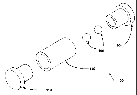
FIG. 1 is an exploded perspective side view of the present omnidirectional
tilt and
vibration sensor, in accordance with a first exemplary embodiment of the
invention.
FIG. 2 is a cross-sectional side view of the first end cap of FIG. 1.
FIG. 3 is a cross-sectional side view of the central member of FIG. 1.
FIG. 4 is a cross-sectional side view of the second end cap of FIG. 1.
FIG. 5 is a flowchart illustrating a method of assembling the omnidirectional
tilt and
vibration sensor of FIG. 1.
FIGS. 6A and FIG. 6B are cross-sectional side views of the sensor of FIG. 1 in
a
closed state, in accordance with the first exemplary embodiment of the
invention.
5a
CA 02594949 2007-07-16
WO 2006/078602
PCT/US2006/001503
FIGS. 7A, 7B, 7C, and 7D are cross-sectional side views of the sensor of FIG.
1 in an
open state, in accordance with the first exemplary embodiment of the
invention.
FIG. 8 is a cross-sectional side view of the present omnidirectional tilt and
vibration
sensor, in accordance with a second exemplary embodiment of the invention.
FIG. 9 is cross-sectional view of a sensor in a closed state, in accordance
with a third
exemplary embodiment of the invention.
DETAILED DESCRIPTION
The following describes an omnidirectional tilt and vibration sensor. The
sensor contains
a minimal number of cooperating parts to ensure ease of assembly and use. FIG.
1 is an
exploded perspective side view of the present omnidirectional tilt and
vibration sensor 100
(hereafter, "the sensor 100"), in accordance with a first exemplary embodiment
of the invention.
Referring to FIG. 1, the sensor 100 contains a first end cap 110, a central
member 140, a
second end cap 160, and multiple weights embodied as a pair of conductive
balls 190 that are
spherical in shape (hereafter, conductive spheres). The first end cap 110 is
conductive, having a
proximate portion 112 and a distal portion 122. Specifically, the first end
cap 110 may be
constructed from a composite of high conductivity and/or low reactivity
metals, a conductive
plastic, or any other conductive material.
FIG. 2 is a cross-sectional side view of the first end cap 110 which may be
referred to for
a better understanding of the location of portions of the first end cap 110.
The proximate portion
112 of the first end cap 110 is circular, having a diameter D1, and having a
flat end surface 114.
A top surface 116 of the proximate portion 112 runs perpendicular to the flat
end surface 114. A
width of the top surface 116 is the same width as a width of the entire
proximate portion 112 of
6
CA 02594949 2007-07-16
WO 2006/078602
PCT/US2006/001503
the first end cap 110. The proximate portion 112 also contains an internal
surface 118 located on
a side of the proximate portion 112 that is opposite to the flat end surface
114, where the top
surface 116 runs perpendicular to the internal surface 118. Therefore, the
proximate portion 112
is in the shape of a disk.
It should be noted that while FIG. 2 illustrates the proximate portion 112 of
the first end
cap 110 having a flat end surface 114 and the proximate portion 162 (FIG. 4)
of the second end
cap 160 having a flat surface 164 (FIG. 4), one having ordinary skill in the
art would appreciate
that the proximate portions 112, 162 (FIG. 4) do not require presence of a
flat end surface.
Instead, the flat end surfaces 114, 164 may be convex or concave. In addition,
instead of being
circular, the first end cap 110 and the second end cap 160 may be square-like
in shape, or they
may be any other shape. Use of circular end caps 110, 160 is merely provided
for exemplary
purposes. The main function of the end caps 110, 160 is to provide a
connection to allow an
electrical charge introduced to the first end cap 110 to traverse the
conductive spheres 190 and be
received by the second end cap 160, therefore, many different shapes and sizes
of end caps 110,
160 may be used as long as the conductive path is maintained.
The relationship between the top portion 116, the flat end surface 114, and
the internal
surface 118 described herein is provided for exemplary purposes.
Alternatively, the flat end
surface 114 and the internal surface 118 may have rounded or otherwise
contoured ends resulting
in the top surface 116 of the proximate portion 112 being a natural rounded
progression of the
end surface 114 and the internal surface 118.
The distal portion 122 of the first end cap 110 is tube-like in shape, having
a diameter D2
that is smaller than the diameter D1 of the proximate portion 112. The distal
portion 122 of the
first end cap 110 contains a top surface 124 and a bottom surface 126. The
bottom surface 126
7
CA 02594949 2007-07-16
WO 2006/078602
PCT/US2006/001503
of the distal portion 122 defines an exterior portion of a cylindrical gap 128
located central to the
distal portion 122 of the first end cap 110. A diameter D3 of the cylindrical
gap 128 is smaller
than the diameter D2 of the distal portion 122.
Progression from the proximate portion 112 of the first end cap 110 to the
distal portion
122 of the first end cap 110 is defined by a step where a top portion of the
step is defined by the
top surface 116 of the proximate portion 112, a middle portion of the step is
defined by the
internal surface 118 of the proximate portion 112, and a bottom portion of the
step is defined by
the top surface 124 of the distal portion 122.
The distal portion 122 of the first end cap 110 also contains an outer surface
130 that
joins the top surface 124 and the bottom surface 126. It should be noted that
while FIG. 2 shows
the cross-section of the outer surface 130 as being squared to the top surface
124 and the bottom
surface 126, the outer surface 130 may instead be rounded or of a different
shape.
As is better shown by FIG. 2, the distal portion 122 of the first end cap 110
is an
extension of the proximate portion 112 of the first end cap 110. In addition,
the top surface 124,
the outer surface 130, and the bottom surface 126 of the distal portion 122
form a cylindrical lip
of the first end cap 110. As is also shown by FIG. 2, the distal portion 122
of the first end cap
110 also contains an inner surface 132, the diameter of which is equal to or
smaller than the
diameter D3 of the cylindrical gap 128. While FIG. 2 illustrates the inner
surface 132 as running
parallel to the flat end surface 114, as is noted hereafter, the inner surface
132 may instead be
concave, conical, or hemispherical.
Referring to FIG. 1, the central member 140 of the sensor 100 is tube-like in
shape,
having a top surface 142, a proximate surface 144, a bottom surface 146, and a
distal surface
148. FIG. 3 is a cross-sectional side view of the central member 140 and may
also be referred to
8
CA 02594949 2007-07-16
WO 2006/078602
PCT/US2006/001503
for a better understanding of the location of portions of the central member
140. It should be
noted that the central member 140 need not be tube-like in shape.
Alternatively, the central
member 140 may have a different shape, such as, but not limited to that of a
square.
The bottom surface 146 of the central member 140 defines a hollow center 150
having a
diameter D4 that is just slightly larger than the diameter D2 (FIG. 2),
thereby allowing the distal
portion 122 of the first end cap 110 to fit within the hollow center 150 of
the central member 140
(FIG. 3). In addition, the top surface 142 of the central member 140 defines
the outer surface of
the central member 140 where the central member 140 has a diameter D5. It
should be noted
that the diameter D1 (i.e., the diameter of the proximate portion 112 of the
first end cap 110) is
preferably slightly larger than diameter D5 (i.e., the diameter of the central
member 140). Of
course, different dimensions of the central member 140 and end caps 110, 160
may also be
provided. In addition, when the sensor 100 is assembled, the proximate surface
144 of the
central member 140 rests against the internal surface 118 of the first end cap
110.
Unlike the first end cap 110 and the second end cap 160, the -central member
140 is not
electrically conductive. As an example, the central member 140 may be made of
plastic, glass,
or any other nonconductive material. In an alternative embodiment of the
invention, the central
member 140 may also be constructed of a material having a high melting point
that is above that
used by commonly used soldering materials. As is further explained in detail
below, having the
central member 140 non-conductive ensures that the electrical conductivity
provided by the
sensor 100 is provided through use of the conductive spheres 190.
Specifically, location of the
central member 140 between the first end cap 110 and the second end cap 160
provides a non-
conductive gap between the first end cap 110 and the second end cap 160.
9
CA 02594949 2007-07-16
WO 2006/078602
PCT/US2006/001503
Referring to FIG. 1, the second end cap 160 is conductive, having a proximate
portion
162 and a distal portion 172. Specifically, the second end cap 160 may be
constructed from a
composite of high conductivity and/or low reactivity metals, a conductive
plastic, or any other
conductive material.
FIG. 4 is a cross-sectional side view of the second end cap 160 which may be
referred to
for a better understanding of the location of portions of the second end cap
160. The proximate
portion 162 of the second end cap 160 is circular, having a diameter D6, and
having a flat end
surface 164. A top surface 166 of the proximate portion 162 runs perpendicular
to the flat end
surface 164. A width of the top surface 166 is the same width as a width of
the entire proximate
portion 162 of the second end cap 160. The proximate portion 162 also contains
an internal
surface 168 located on a side of the proximate portion 162 that is opposite to
the flat end surface
164, where the top surface 166 runs perpendicular to the internal surface 168.
Therefore, the
proximate portion 162 is in the shape of a disk.
The relationship between the top portion 166, the flat end surface 164, and
the internal
surface 168 described herein is provided for exemplary purposes.
Alternatively, the flat end
surface 164 and the internal surface 168 may have rounded or otherwise
contoured ends resulting
in the top surface 166 of the proximate portion 162 being a natural rounded
progression of the
end surface 164 and the internal surface 168.
The distal portion 172 of the second end cap 160 is tube-like is shape, having
a diameter
D7 that is smaller than the diameter D6 of the proximate portion 162. The
distal portion 172 of
the second end cap 160 contains a top surface 174 and a bottom surface 176.
The bottom surface
176 of the distal portion 172 defines an exterior portion of a cylindrical gap
178 located central
CA 02594949 2007-07-16
WO 2006/078602
PCT/US2006/001503
to the distal portion 172 of the second end cap 160. A diameter D8 of the
cylindrical gap 178 is
smaller than the diameter D7 of the distal portion 172.
Progression from the proximate portion 162 of the second end cap 160 to the
distal
portion 172 of the second end cap 160 is defined by a step where a top portion
of the step is
defined by the top surface 166 of the proximate portion 162, a middle portion
of the step is
defined by the internal surface 168 of the proximate portion 162, and a bottom
portion of the step
is defined by the top surface 174 of the distal portion 172.
The distal portion 172 of the second end cap 160 also contains an outer
surface 180 that
joins the top surface 174 and the bottom surface 176. It should be noted that
while FIG. 4 shows
the cross-section of the outer surface 180 as being squared to the top surface
174 and the bottom
surface 176, the outer surface 180 may instead be rounded or of a different
shape.
As is better shown by FIG. 4, the distal portion 172 of the second end cap 160
is an
extension of the proximate portion 162 of the second end cap 160. In addition,
the top surface
174, the outer surface 180, and the bottom surface 176 of the distal portion
172 form a
cylindrical lip of the second end cap 160. As is also shown by FIG. 4, the
distal portion 172 of
the second end cap 160 also contains an inner surface 182, the diameter of
which is equal to or
smaller than the diameter D8 of the cylindrical gap 178. While FIG. 4
illustrates the inner
surface 182 as running parallel to the flat end surface 164, the inner surface
182 may instead be
concave, conical, or hemispherical.
It should be noted that dimensions of the second end cap 160 are preferably
the same as
dimensions of the first end cap 110. Therefore, the diameter D4 of the central
member 140
hollow center 150 is also just slightly larger that the diameter D7 of the
second end cap 160,
thereby allowing the distal portion 172 of the second end cap 160 to fit
within the hollow center
11
CA 02594949 2007-07-16
WO 2006/078602
PCT/US2006/001503
150 of the central member 140. In addition, the diameter D6 (i.e., the
diameter of the proximate
portion 162 of the second end cap 160) is preferably slightly larger that
diameter DS (i.e., the
diameter of the central member 140). Further, when the sensor 100 is
assembled, the distal
surface 148 of the central member 140 rests against the internal surface 168
of the second end
cap 160.
Referring to FIG. 1, the pair of conductive spheres 190, including a first
conductive
sphere 192 and a second conductive sphere 194, fit within the central member
140, within a
portion of the cylindrical gap 128 of the first distal portion 122 of the
first end cap 110, and
within a portion of the cylindrical gap 178 of the second end cap 160.
Specifically, the inner
surface 132, bottom surface 126, and outer surface 130 of the first end cap
110, the bottom
surface 146 of the central member 140, and the inner surface 182, bottom
surface 176, and outer
surface 180 of the second end cap 160 form a central cavity 200 of the sensor
100 where the pair
of conductive spheres 190 are confined.
Further illustration of location of the conductive spheres 190 is provided and
illustrated
with regard to FIGS. 6A, 6B, and 7A-7D. It should be noted that, while the
figures in the present
disclosure illustrate both of the conductive spheres 190 as being
substantially symmetrical,
alternatively, one sphere may be larger that the other sphere. Specifically,
as long as the
conductive relationships described herein are maintained, the conductive
relationships may be
maintained by both spheres being larger, one sphere being larger than the
other, both spheres
being smaller, or one sphere being smaller. It should be noted that the
conductive spheres 190
may instead be in the shape of ovals, cylinders, or any other shape that
permits motion within the
central cavity in a manner similar to that described herein.
12
CA 02594949 2007-07-16
WO 2006/078602
PCT/US2006/001503
Due to minimal components, assembly of the sensor 100 is quite simplistic.
Specifically,
there are four components, namely, the first end cap 110, the central member
140, the conductive
spheres 190, and the second end cap 160. FIG. 5 is a flowchart illustrating a
method of
assembling the omnidirectional tilt and vibration sensor 100 of FIG. 1. It
should be noted that
any process descriptions or blocks in flowcharts should be understood as
representing modules,
segments, portions of code, or steps that include one or more instructions for
implementing
specific logical functions in the process, and alternate implementations are
included within the
scope of the present invention in which functions may be executed out of order
from that shown
or discussed, including substantially concurrently or in reverse order,
depending on the
functionality involved, as would be understood by those reasonably skilled in
the art of the
present invention.
As is shown by block 202, the distal portion 122 of the first end cap 110 is
fitted within
the hollow center 150 of the central member 140 so that the proximate surface
144 of the central
member 140 is adjacent to or touching the internal surface 118 of the first
end cap 110. The
conductive spheres 190 are then positioned within the hollow center 150 of the
central member
140 and within a portion of the cylindrical gap 128 (block 204). The distal
portion 172 of the
second end cap 160 is then fitted within the hollow center 150 of the central
member 140, so that
the distal surface 148 of the central member 140 is adjacent to or touching
the internal surface
168 of the second end cap 160 (block 206).
In accordance with an alternative embodiment of the invention, the sensor 100
may be
assembled in an inert gas, thereby creating an inert environment within the
central cavity 200,
thereby reducing the likelihood that the conductive spheres 190 will oxidize.
As is known by
those having ordinary skill in the art, oxidizing of the conductive spheres
190 would lead to a
13
CA 02594949 2007-07-16
WO 2006/078602
PCT/US2006/001503
decrease in the conductive properties of the conductive spheres 190. In
addition, in accordance
with another alternative embodiment of the invention, the first end cap 110,
the central member
140, and the second end cap 160 may be joined by a hermetic seal, thereby
preventing any
contaminant from entering the central cavity 200.
The sensor 100 has the capability of being in a closed state or an open state,
depending on
location of the conductive spheres 190 within the central cavity 200 of the
sensor 100. FIG. 6A
and FIG. 6B are cross-sectional views of the sensor 100 of FIG. 1 in a closed
state, in accordance
with the first exemplary embodiment of the invention. In order for the sensor
100 to be
maintained in a closed state, an electrical charge introduced to the first end
cap 110 is required to
traverse the conductive spheres 190 and be received by the second end cap 160.
Referring to FIG. 6A, the sensor 100 is in a closed state because the first
conductive
sphere 192 is touching the bottom surface 126 of the first end cap 110, the
conductive spheres
192, 194 are touching, and the second conductive sphere 194 is touching the
bottom surface 176
and inner surface 182 of the second end cap 162, thereby providing a
conductive path from the
first end cap 110, through the conductive spheres 190, to the second end cap
160. Referring to
FIG. 6B, the sensor 100 is in a closed state because the first conductive
sphere 192 is touching
the bottom surface 126 and inner surface 132 of the first end cap 110, the
conductive spheres
192, 194 are touching, and the second conductive sphere 194 is touching the
bottom surface 176
of the second end cap 162, thereby providing a conductive path from the first
end cap 110,
through the conductive spheres 190, to the second end cap 160. Of course,
other arrangements
of the first and second conductive spheres 190 within the central cavity 200
of the sensor 100
may be provided as long as the conductive path from the first end cap 110 to
the conductive
spheres 190, to the second end cap 160 is maintained.
14
CA 02594949 2007-07-16
WO 2006/078602
PCT/US2006/001503
FIGS. 7A ¨ FIG. 7D are cross-sectional views of the sensor 100 of FIG. 1 in an
open
state, in accordance with the first exemplary embodiment of the invention. In
order for the
sensor 100 to be maintained in an open OFF state, an electrical charge
introduced to the first end
cap 110 cannot traverse the conductive spheres 190 and be received by the
second end cap 160.
Referring to FIGS. 7A ¨ 7D, each of the sensors 100 displayed are in an open
state because the
first conductive sphere 192 is not in contact with the second conductive
sphere 194. Of course,
other arrangements of the first and second conductive spheres 190 within the
central cavity 200
of the sensor 100 may be provided as long as no conductive path is provided
from the first end
cap 110 to the conductive spheres 190, to the second end cap 160.
FIG. 8 is a cross-sectional side view of the present omnidirectional tilt and
vibration
sensor 300, in accordance with a second exemplary embodiment of the invention.
The sensor
300 of the second exemplary embodiment of the invention contains a first nub
302 located on the
flat end surface 114 of the first end cap 110 and a second nub 304 located on
a flat end surface
164 of the second end cap 160. The nubs 302, 304 provide a conductive
mechanism for allowing
the sensor 300 to connect to a printed circuit board (PCB) landing pad, where
the PCB landing
pad has an opening cut into it allowing the sensor to recess into the opening.
Specifically,
dimensions of the sensor in accordance with the first exemplary embodiment and
the second
exemplary embodiment of the invention may be selected so as to allow the
sensor to fit within a
landing pad of a PCB. Within the landing pad there may be a first terminal and
a second
terminal. By using the nubs 302, 304, fitting the sensor 300 into landing pad
may press the first
nub 302 against the first terminal and the second nub 304 against the second
terminal. Those
having ordinary skill in the art would understand the basic structure of a PCB
landing pad,
therefore, further explanation of the landing pad is not provided herein.
CA 02594949 2007-07-16
WO 2006/078602
PCT/US2006/001503
It should be noted that the sensor of the first and second embodiments have
the same
basic rectangular shape, thereby contributing to ease of preparing a PCB for
receiving the sensor
100, 300. Specifically, a hole may be cut in a PCB the size of the sensor 100
(i.e., the size of the
first and second end caps 110, 160 and the central member 140) so that the
sensor 100 can drop
into the hole, where the sensor is prevented from falling through the hole
when caught by the
nubs 302, 304 that land on connection pads. In the first exemplary embodiment
of the invention,
where there are no nubs, the end caps 110, 160 may be directly mounted to the
PCB.
In accordance with another alternative embodiment of the invention, the two
conductive
spheres may be replaced by more than two conductive spheres, or other shapes
that are easily
inclined to roll when the sensor 100 is moved.
FIG. 9 is cross-sectional view of a sensor 400 in a closed state, in
accordance with a third
exemplary embodiment of the invention. As is shown by FIG. 9, an inner surface
412 of a first
end cap 410 is concave is shape. In addition, an inner surface 422 of a second
end cap 420 is
concave in shape. The senso-r 400 of FIG. 9 also contains a first nub 430 and
a second nub 432
that function in a manner similar to the nubs 302, 304 in the second exemplary
embodiment of
the invention. Having a sensor 400 with concave inner surfaces 412, 422 keeps
the sensor 400 in
a normally closed state due to the shape of the inner surfaces 412, 422 in
combination with
gravity causing the conductive spheres 192, 194 to be drawn together.
It should be emphasized that the above-described embodiments of the present
invention
are merely possible examples of implementations, merely set forth for a clear
understanding of
the principles of the invention. Many variations and modifications may be made
to the above-
described embodiments of the invention without departing substantially from
the spirit and
principles of the invention. All such modifications and variations are
intended to be included
16
CA 02594949 2007-07-16
WO 2006/078602
PCT/US2006/001503
herein within the scope of this disclosure and the present invention and
protected by the
following claims.
17