Note: Descriptions are shown in the official language in which they were submitted.
CA 02595354 2007-07-19
WO 2006/077105 PCT/EP2006/000424
System and method for optically imaging objects on a detection device by means
of
a pinhole aperture
Field of the invention:
The invention concerns systems for optically imaging objects, in particular
information-carrying optical patterns or codes, on a detection device and in
particular on a CCD or CMOS element with the aid of a pinhole aperture. The
invention especially concerns systems that have special devices which
substantially
compensate the imaging defects caused by the pinhole aperture and in
particular
the system-inherent peripheral decrease in brightness of an image of the
object
formed by a pinhole aperture on the detection device.
In addition the invention concerns systems for capturing optical information
which
comprise such a system for optically imaging an object that carries optical
information and an in-line evaluation device which collects the optical
information
of the object from the image of the object formed on the detector device and
provides this information for further processing or display.
In addition the invention concerns test element analytical systems comprising
at
least one test element and an evaluation device which contain such systems
according to the invention for collecting optical information.
Finally the invention concerns methods for optically imaging objects on a
detection
device by mmxeai s of a pinhole aperture which can substantially comWeftsate
the
imaging defects caused by the pinhole aperture and in particular the system-
inherent peripheral decrease in brightness of an image of the object formed by
a
pinhole aperture on the detection device.
CA 02595354 2007-07-19
WO 2006/077105 PCT/EP2006/000424
-2-
State of the art:
The optical imaging of objects on detection devices plays a major role in many
technical fields. Thus the optical imaging of one-dimensional or two-
dimensional
optical patterns on detection devices that are usually in special reading
systems such
as code readers or scanners, is used to collect information on the objects
which
carry these optical patterns and to transfer the information to an in-line
evaluation
system.
Optical patterns which are often used to store or transfer information are for
example one-dimensional (1 D, for example barcodes) or two-dimensional (2 D,
for example data matrix codes) codes which are applied to objects, for example
printed onto or glued onto objects and contain information on this object. In
this
case the information is coded in the optical pattern of the code. An image
thereof is
formed on a detection device which firstly records the image of the pattern.
Subsequently the information of the imaged object can be collected therefrom
and
provided for further processing or display. Thus for example structural units,
individual components, intermediate and also final products can be
unequivocally
identified and controlled with such a code which, among others, enables a
control
of production and storage and a traceability of products if errors should
occur.
Typical fields of application of such codes are storage and materials-handling
technology, quality assurance, material monitoring, production control, sample
identification in pharmaceutics and the health system, in the automobile
industry,
in chemical and biomedical analyzers and for document handling.
Such optical systems are also used to record optical patterns especially in
chemical
and diagnostic analytical systems and especially in test element analytical
systems.
In such test element analytical systems optical codes which are on the
respective test
element or on an object that is specially provided for this purpose such as a
batch-
specific coding object, are used primarily to deliver specific information to
the
evaluation device on the test that is being used in each case and/or the
special test
element. Such test element analytical systems are described for example in the
German Patent Application with the file number 102004011648.2.
CA 02595354 2007-07-19
WO 2006/077105 PCT/EP2006/000424
-3-
The optical reading systems used in industrial applications usually employ
lens
optics in reflection optical methods which form an image of the optical
pattern on a
detection device. Other designs are for example realized in scanners which use
partially transparent optical patterns or codes in a transmission process.
Whereas
one-dimensional codes can usually be recorded relatively simply by means of
line
sensors or scanners that move relatively to the code-carrying object, two-
dimensional optical patterns such as 2D codes are firstly imaged on a
detection
device and these images are subsequently evaluated usually by means of special
software algorithms. Such reading systems for two-dimensional optical patterns
usually employ optical matrix sensors such as CCD or CMOS sensors as detection
devices.
For a good imaging quality of the imaging system it is important that these
systems
have imaging properties that result in a substantially uniform system-inherent
brightness distribution in the detection plane. In this connection the term
system-
inherent brightness distribution in the detection plane is understood to mean
that it
refers to the brightness distribution of the image of a uniform object and in
particular a homogeneous and especially unifurrnally structured arid uniformly
coloured surface on a detection device which is located in the detection
plane. Such
a brightness distribution allows information to be obtained on the fundamental
imaging properties of the optical system. An image of such a uniform object
can be
regarded as a type of background image which represents the system-inherent
imaging properties including its system-inherent imaging defects. An object
that is
to be imaged which carries information must be distinguishable from such a
system-inherent background image for example in the form of defined areas of a
different brightness or colour. If a system-inherent background image already
results in appreciable differences in brightness in the detection plane, these
system-
inherent differences in brightness would be superimposed on the differences in
brightness that are due to the actual information-carrying object that is to
be
imaged and are desired and necessary for information transfer, for example in
the
form of areas that are too light or dark. This would considerably complicate,
falsify
or prevent the acquisition and evaluation of the true information to be
transferred.
CA 02595354 2007-07-19
WO 2006/077105 PCT/EP2006/000424
-4-
Various solutions have been proposed in the prior art to achieve the most
homogeneous system-inherent brightness distribution in the detection plane:
Thus for example the 2D code reader "Quadrus" from the Microsan Company
(Freising, Germany) has 20 individual high-performance LEDs as light sources
to
illuminate the object as homogeneously as possible.
The German laid-open document DE 4221069 describes an optical device for
imaging optical patterns such as a barcode that are imaged on a photosensor.
The
optical device comprises an imaging lens to image the barcode and a CCD line
sensor to record and evaluate the information of the image of the barcode. The
system also has an attenuation device that is arranged between the barcode and
the
line sensor and is designed such that the system-inherent brightness
distribution on
the sensor becomes more uniform despite the construction-related influence by
the
imaging lens. In this connection DE 4221069 teaches attenuation elements which
comprise an optical element which is able to attenuate the intensity of
certain
spatial areas of a light beam that impinges on the line sensor after being
emitted
from the object to be imaged. In this connection DE 4221069 teaches in
particular
mirror elements that are provided with a coating which has a lower refractive
index
in the central area than in the periphery and are thus suitable as attenuation
elements according to the invention. Furthermore DE 4221069 teaches ND
(neutral
density) filters as attenuation elements with a lower transmission factor in
the
central area than in the periphery which can be used as light attenuating
filters in
the optical path between the code to be imaged and the detection device.
Other factors have to be taken into consideration for an application of
imaging
systems especially in mobile instruments or hand-held systems such as hand
scanners or portable test element analytical systems:
- Since such systems are often manufactured in large numbers it is
advantageous to integrate imaging systems that are as simple and cheap as
possible into these systems or instruments. They must nevertheless fulfil
certain requirements with regard to the imaging quality in order to ensure
CA 02595354 2007-07-19
WO 2006/077105 PCT/EP2006/000424
-5-
the optical information which is contained in the objects to be imaged is
accurately recorded and evaluated.
- Many of the conventional systems which employ a scanning movement
relative to the object to be imaged have a relatively large constructed space
which, among others, is due to their lens systems and the devices that
control the movement of the object relative to the detection device. Since
especially test element analytical systems are often designed as portable
hand-held instruments, it is desirable that such systems have the smallest
possible constructional size that should be in the range of a few cubic
centimetres.
- Simple and cheap imaging systems usually employ a transmission method
which means that the object to be imaged is irradiated by a light source and
imaged on a detection device which is located on the side opposite to the
light source. It is inherent to the system that such systems require a large
constructional space since the light source, object to be imaged and
detection device have to be arranged one behind the other and they are
therefore only of limited suitability for use in portable systems. Moreover,
the object to be imaged must have certain optical properties in order for
such transmission methods to be used at all. Thus for example optical codes
must have at least partially transparent areas in order that their information
can be read by such systems. Consequently such imaging systems are
unsuitable for many fields of application.
No systems aie known from the prior art for optically imaging objects which
are
characterized by a combination of a very simple and cheap design, the smallest
possible structural space, the ability to form an image of the object to be
imaged on
the detection device without a movement of the imaging system relative to the
objeU and very reliable reading. In particular the known imaging systems are
only
of limited suitability for incorporation into small and portable systems and
in
particular into diagnostic test element analytical systems. In particular no
simple
imaging systems are known which achieve a very uniform system-inherent
brightness distribution in the detection plane using simple and cost-efficient
means.
CA 02595354 2011-06-16
-6-
Object of the invention:
The object of the present invention is to provide systems and methods for
optically
imaging an object which avoid the disadvantages of the prior art. The object
of the
present invention is in particular to provide systems and methods for imaging
optical patterns and in particular codes which fulfil the aforementioned
requirements for such imaging systems for use in portable test element
analytical
systems.
Another object of the present invention is to provide a simple and cost-
efficient
system for optically imaging objects on a detection device in a compact design
which has a system-inherent brightness distribution in the detection plane
that is as
uniform as possible.
Another object of the present invention is to provide systems for recording
and
processing optical information which, in addition to an imaging system, have
additional devices which record the optical information of the object that are
imaged on the detection device and provide this information for further
processing
or display.
Another object of the present invention is to provide test element analytical
systems
which comprise at least one test element which encodes information in the form
of
an optical pattern and at least one evaluation device which has a system for
recording and processing this optical information. Finally another object of
the
present invention is to provide methods for optically imaging objects on a
detection
device in which the system-inherent brightness distribution is ensured tube as
uniform as possible in the detection plane.
Solution according to the invention:
These objects are achieved according to the invention by providing a system
for
optically imaging an object by means of a pinhole aperture. Such an imaging
system
is based on the principle of the pinhole camera or camera obscura and has a
pinhole
aperture which is used to form an image of the object on the detection device.
The
principle of imaging by means of a pinhole aperture is for example explained
in
CA 02595354 2011-06-16
-6a-
In accordance with one aspect of the present invention, there is provided a
pinhole camera
system for optically imaging an object comprising: a detection device located
in a detection
plane; a pinhole aperture configured in accordance with a pinhole camera
principle to image
the object located in an object plane onto the detection device; an
illumination device for
illuminating the object; and an optical attenuation element arranged between
the illumination
device and the object plane, which optical attenuation element is configured
to essentially
compensate for system-inherent imaging defects caused by the pinhole aperture.
In accordance with another aspect of the present invention, there is provided
a method for
optically imaging an object comprising: providing an object located in an
object plane;
providing a detection device located in a detection plane; providing an
illumination device;
providing an optical attenuation element arranged between the illumination
device and the
object plane; illuminating the object with the illumination device; and
imaging the object onto
the detection device by a pinhole aperture configured in accordance with a
pinhole camera
principle, wherein the optical attenuation element essentially compensates for
system-inherent
imaging defects caused by the pinhole aperture.
In accordance with yet another aspect of the present invention, there is
provided a pinhole
camera system for optically imaging an object comprising: a detection device
located in a
detection plane; a pinhole aperture configured in accordance with a pinhole
camera principle
to image an object located in an object plane onto the detection device; an
illumination device
for illuminating the object; and an optical attenuation element arranged
between the
illumination device and the object plane, which optical attenuation element is
configured to
essentially compensate for system-inherent imaging defects caused by the
pinhole aperture,
wherein the optical attenuation element is in the form of a film mask which
has one or more
aperture structures, and the object is imaged on the detection device by
reflection-optical
methods and the pinhole aperture is integrated into the film mask.
In accordance with still another aspect of the present invention, there is
provided a system for
optically imaging an object which is located in an object plane comprising: a
detection device
which is located in a detection plane, a pinhole aperture located between the
object plane and
the detection plane to image the object onto the detection device, and an
illumination device
for illuminating the object in the object plane, characterized in that optical
attenuation
elements are arranged between the illumination device and the object plane
which change the
illumination of the object by the illumination device such that the central
areas of the object
are illuminated at a lower illumination intensity than the peripheral areas of
the object to
CA 02595354 2011-06-16
-6b-
essentially compensate the system-inherent peripheral decrease in brightness
of an image of
the object imaged by the pinhole aperture onto the detection device.
In accordance with yet still another aspect of the present invention, there is
provided a method
for optically imaging an object which is located in an object plane onto a
detection device
which is located in a detection plane where the object is illuminated by an
illumination device
and the object is imaged onto the detection device by a pinhole aperture,
characterized in that
optical attenuation elements are arranged between the illumination device and
the object plane
which change the illumination of the object by the illumination device such
that the central
areas of the object are illuminated at a lower illumination intensity than the
peripheral areas of
the object to essentially compensate the imaging defects caused by the pinhole
aperture and in
particular the system-inherent peripheral decrease in brightness of an image
of the object
formed by a pinhole aperture on the detection device.
Solution according to the invention:
These objects are achieved according to the invention by providing a system
for optically
imaging an object by means of a pinhole aperture. Such an imaging system is
based on the
principle of the pinhole camera or camera obscura and has a pinhole aperture
which is used to
form an image of the object on the detection device. The principle of imaging
by means of a
pinhole aperture is for example explained in
CA 02595354 2007-07-19
WO 2006/077105 PCT/EP2006/000424
-7-
more detail in the "Lexikon der Optik" (Spektrum Akademischer Verlag,
Heidelberg, Germany).
A major advantage of imaging systems based on the pinhole camera principle is
that
no lenses are required to form an image of the object. Lenses and systems of
several
lenses have construction-inherent imaging defects which considerably reduce
the
quality of the image and can thus make subsequent information processing
impossible or erroneous. Construction-inherent imaging defects of optical
lenses or
lens systems are for example spherical aberration, chromatic aberration,
colour
enlargement errors, coma or asymmetry defects, astigmatism, image field
curvature,
vignetting, distortion or diffraction. It has been possible to largely avoid
these
imaging defects by the use of lensless imaging methods.
An image created by means of a pinhole aperture essentially does not have
these
construction-inherent imaging defects of a lens with the exception of a slight
vignetting caused by the geometry which ensures an imaging of the object which
is
as free as possible of distortion that is the basis for information transfer
that is as
free of errors as possible. In particular images based on the pinhole camera
principle are characterized by an almost infinite depth of focus.
Another advantage of imaging methods according to the pinhole camera principle
is that it enables a simple and cost-effective system to be provided for
imaging
objects in a compact design which does not require complex and expensive lens
systems and enables considerably smaller designs.
However, conventional pinhole camera systems have a system-inherent decrease
in
brightness towards the edge of the image formed on the detection plane which
is
also referred to within the scope of the present invention as peripheral
decrease in
brightness. This system-inherent decrease in brightness towards the periphery
of the
image is largely due to diffraction phenomena at the pinhole aperture and is
particularly perceptible at large viewing angles since it is proportional to
the fourth
power of the half cosine of the viewing angle. Thus at a viewing angle of 90
only
25 % of the light intensity striking the middle of the image would impinge on
the
CA 02595354 2007-07-19
WO 2006/077105 PCT/EP2006/000424
-8-
detection plane at the right and left edge of the image (cos(90 /2)4 = 0.25)
which
would correspond to a decrease in brightness towards the edges of 2 aperture
stops.
This system-inherent decrease in brightness towards the periphery of the image
has
previously prevented a wider use of optical methods according to the pinhole
camera principle especially in information-carrying optical systems because
there is
a large degree of inhomogeneity of the system-inherent brightness distribution
depending on the position of the image point relative to the centre of the
image. As
a result these system-inherent brightness effects may be superimposed on the
image
of the object in the detection plane since, due to the pinhole aperture
principle,
central areas of the object are imaged more brightly than peripheral areas.
Central
areas of the object or image are areas which are near to the optical axis of
the
imaging system, peripheral areas of the object or the image are areas that are
further
removed from the optical axis of the imaging system. If an optical pattern and
in
particular an optical code is not imaged in the detection plane with a
substantially
uniform system-inherent brightness distribution, it is for example difficult
to
specify threshold values to differentiate between light or dark areas of the
pattern so
that it may not be possible to correctly read the information contained in the
optical
pattern or code.
Methods are known in which a system-inherent brightness distribution in the
detection plane that is as homogeneous as possible is achieved by placing
optical
elements between the object to be imaged and the detection plane which
diminish
the intensity of the light emitted from the object more strongly in the
central areas
in comparison to the peripheral areas of the image. DE 4221069 describes such
elements. A particular disadvantage of this arrangement is that such optical
elements have to be additionally placed in the optical path between the object
and
detection plane which increases the depth of the structure and the complexity
of
this imaging system.
It was surprisingly found within the scope of the present invention that the
system-
inherent imaging defects caused by the use of a pinhole aperture can be
substantially compensated by an optical imaging system according to the
invention
CA 02595354 2007-07-19
WO 2006/077105 PCT/EP2006/000424
-9-
and a substantially uniform system-inherent brightness distribution in the
detection
plane can be achieved with at the same time a compact design.
The solution according to the invention is to provide a system for optically
imaging
an object which is located in an object plane comprising a detection device
which is
located in a detection plane, a pinhole aperture for imaging the object on the
detection device and an illumination device for illuminating the object,
wherein
optical attenuation elements are arranged between the illumination device and
the
object plane which substantially compensate the imaging defects caused by the
pinhole aperture and in particular the system-inherent peripheral decrease in
brightness of an image of the object imaged by a pinhole aperture on the
detection
device. In a preferred embodiment the optical attenuation elements are
designed
such that they result in a substantially uniform brightness distribution of
the image
of the object formed on the detection device when imaging a uniform object and
in
particular a homogeneous surface through the pinhole aperture.
The optical attenuation elements are located according to the invention
between the
illumination devices and the object plane so that the use of such optical
attenuation
elements affects the intensity distribution of the illumination of the object.
This is in
contrast to the systems and methods described in the prior art which describe
such
attenuation elements between the object and detection plane and in which the
illumination of the object is initially substantially homogeneous.
In this connection a particular advantage over the prior art is that these
optical
attenuation elements do not have to be additionally placed in the optical path
between the object and detection plane but can instead be placed between the
illumination devices already present and the object plane without increasing
the
constructional size of the overall system. In a particularly preferred
embodiment the
optical attenuation elements are designed such that they change the
illumination of
the object by the illumination device such that the central areas of the
object are
illuminated at a lower illumination intensity than the peripheral areas of the
object.
CA 02595354 2007-07-19
WO 2006/077105 PCT/EP2006/000424
-10-
Surprisingly such an illumination is able to substantially compensate the
imaging
defects caused by the pinhole aperture and in particular the system-inherent
peripheral decrease in brightness of an image of the object formed by a
pinhole
aperture on the detection device, and a substantially uniform system-inherent
brightness distribution is achieved in the detection plane. The optical
attenuation
elements and their arrangement according to the invention changes the
illumination of the object by the illumination device in such a manner that
the
central areas of the object are illuminated at a lower light intensity than
the
peripheral areas of the object. As a result of the subsequent imaging of the
object
illuminated in this manner by means of the pinhole aperture, the central areas
of
the object are system-inherently imaged with a higher brightness than the
peripheral areas of the object on the detection device. Surprisingly the
superimposition of the two effects, the weaker illumination according to the
invention of the central areas of the object and the system-inherent imaging
of
central areas of the object at a higher light intensity by the pinhole
aperture can
result in a substantially uniform system-inherent brightness distribution of
the
image of the object to be imaged on the detection device by the imaging system
according to the invention. This is the basis for an error-free and reliable
evaluation
of the optical information of the imaged object.
The compensation according to the invention of the system-inherent imaging
defects does not necessarily have to be complete. For many applications it is
sufficient to reduce these imaging defects to a certain degree. Thus for
example in
the case of imaging a black-white code on a sensor, it may be sufficient to
compensate the system-inherent more light intensive imaging of central areas
of the
object by the pinhole aperture to such an extent that the superimposition of
the
system-inherent brightness distribution on the image of the black-white
pattern in
the detection plane still leads to an image from which the original
information can
be recorded which in some cases may also involve the use of other methods such
as
defining threshold values or grey value spreading. The term uniform brightness
distribution in the detection plane should be understood in the same sense.
CA 02595354 2007-07-19
WO 2006/077105 PCT/EP2006/000424
-11-
In principle all light sources including natural light sources such as
sunlight or
daylight can be used as illumination devices within the sense of the present
invention. Artificial light sources of a substantially constant brightness
such as
filament lamps, glow lamps, discharge or induction lamps can be preferably
used to
ensure that the object to be imaged is illuminated as uniformly and
reproducibly as
possible. Light emitting diodes can be particularly preferably used as
illumination
devices especially for use in portable systems since they have the advantages
of a
very small constructed space, a low power consumption, a long life-time with a
substantially constant light emission, a high shock resistance and the ability
to be
operated with direct voltage.
In a preferred embodiment several individual light sources are used as an
illumination device which in their entirety act to illuminate the object. If
the object
is illuminated by several light sources from different spatial directions, the
respective light beams from the individual light sources impinging on a point
of the
object add up to a total light intensity at this point on the object. Such
oblique
arrangements of several light sources are especially advantageous when
importance
is attached to the smallest possible constructional depth of the optical
system for
example in the case of portable systems. Such an oblique arrangement of
several
light sources at an angle to the optical axis of the system that is not equal
to 0 has
an additional advantage since it can prevent the imaging of the object from
being
affected by direct reflections and avoid a shadowing of certain areas of the
object
especially in the case of three-dimensional objects.
In a preferred embodiment the object is imaged by ineaiis of reflection
optical
methods. Imaging systems that are based on reflection optical methods are
especially suitable for use in portable systems since this enables a very
compact
design to be achieved. In the case of reflection optical methods, the surface
of the
object to be imaged is illuminated by illumination devices. The light
reflected from
the surface of the object is imaged by an imaging system, in the present case
by a
pinhole aperture, onto a detection device. In contrast to transmission optical
methods in which the object is illuminated from the rear side, illumination of
the
surface of the object enables the illumination devices to be positioned on the
side of
CA 02595354 2007-07-19
WO 2006/077105 PCT/EP2006/000424
-12-
the object plane which faces the detection plane which thus enables a
particularly
space saving construction of the imaging system.
In principle all devices can be used as optical attenuation elements in the
sense of
the present invention which are able to substantially compensate the system-
inherent imaging defects caused by the pinhole aperture and in particular the
system-inherent peripheral decrease in brightness of an image of the object
imaged
by a pinhole aperture onto the detection device. In principle all devices can
be used
as optical attenuation elements in the sense of the present invention which
result in
a substantially uniform system-inherent brightness distribution in the
detection
plane.
In a particularly preferred embodiment the optical attenuation elements are in
the
form of aperture structures which are composed of concentric lines of low
transmission and intermediate areas of high transmission, the widths and/or
distances between them being designed such that the central areas of the
object are
illuminated at a lower light intensity than the peripheral areas of the
object.
Such aperture structures are described for example in WO 84/00620. WO 84/00620
describes aperture structures made of diffusely light-permeable substrates on
the
surfaces of which a plurality of light-impermeable concentric circular lilies
is
applied. In order to achieve the desired spatially differentiated light
attenuation, the
spacing of the equally wide circular lines increases continuously towards the
outside
so that the outer areas of the aperture structure are more light permeable
than the
central areas. In another embodiment the spacing of the circular lines is kept
constant whereas the width of these circular lines decreases continuously
towards
the outside so that the outer areas of the aperture structure are more light
permeable than the central areas. Of course combinations of circular lines of
different widths and different spacing between the respective circular lines
are also
conceivable which likewise have the effect that the central areas of the
object are
illuminated at a lower light intensity than the peripheral areas of the
object. In
addition, to such aperture structures which have defined areas of different
light
permeability, aperture structures can also be used according to the invention
which
CA 02595354 2007-07-19
WO 2006/077105 PCT/EP2006/000424
- 13-
achieve a spatially differentiated light attenuation by the fact that their
light
permeability changes substantially continuously and in particular increases
from
the centre towards the peripheral areas. This can for example be a circular
aperture
structure which has a centre that is only slightly or not light permeable
which
towards the outside adjoins areas that are more and more light permeable.
These
areas can merge continuously into one another or be formed as discrete areas.
Depending on the wavelength and composition of the light used for
illumination, it
is possible to also use different colour tones in addition to different
brightnesses or
shades of grey to achieve different light permeabilities. In addition areas
having
different light-scattering or reflecting properties, for example transparent
and
diffusely light-scattering areas, maybe suitable for achieving a spatially
differentiated light attenuation. Also combinations of the various embodiments
that
have been mentioned are possible in order to achieve a spatially
differentiated
attenuation of the illuminating light.
Such aperture structures according to the invention do not necessarily have to
be
constructed as concentric circles or be rotationally symmetrical. Other
geometric
arrangements of areas of different light permeability can also be used
according to
the invention as aperture structures to achieve a spatially differentiated
light
attenuation. If for example the object is not illuminated directly in the
optical axis
of the system but rather laterally displaced thereto, it may be advantageous
to
appropriately adapt the aperture structures. This can for example be achieved
by the
fact that the distance and/or the width of light attenuating lines is
different. in the
areas of the aperture structure which face towards the object to be
illuminated than
in the areas of the aperture structure that face away from the object. Thus in
the
case of an oblique arrangement of the light source, it is also possible to
achieve an
illumination of the object according to the invention which is substantially
independent of the spatial arrangement of the light source.
The areas of different light permeability of the aperture structures can be
manufactured by various technologies known to a person skilled in the art.
Such
technologies can for example be based on exposure methods, photolithographic
methods, laser ablation methods, metal laser methods, coating techniques,
printing
CA 02595354 2007-07-19
WO 2006/077105 PCT/EP2006/000424
-14-
techniques, etching techniques or mechanical machining processes such as
punching, drilling or milling.
In addition to such aperture structures it is also possible according to the
invention
to use optical elements such as lenses or mirrors as optical attenuation
elements.
Optical filters such as ND filters can also be used according to the invention
as
optical attenuation elements. Such embodiments are described among others in
DE 4221069.
If several individual light sources are used to illuminate the object, it may
also be
advantageous to use optical attenuation elements that have been optimized
accordingly. In a particularly preferred embodiment the illumination device
contains several individual light sources in front of which optical
attenuation
elements are arranged in such a manner Thal as a result of the superimposition
of
the light intensities of the individual light sources in the object plane, the
central
areas of the object are illuminated at a lower light intensity than the
peripheral areas
of the object. Since the individual surface points of the object are at
different
distances from the individual light sources and their light beams can impinge
at
different angles, it is nevertheless possible to achieve an illumination of
the object
according to the invention by modifying the aperture structures while taking
into
account the respective illumination situation. Such a design and arrangement
of the
optical attenuation elements that is optimized with regard to the respective
illumination situation can he calculated using geometric and iterative methods
known to a person skilled in the art for example with the aid of computer
programs
such as ASAP (Breault Research Organization, Tucson, Arizona) or Trace Pro
(Light Tec> Hyeres, France).
In a preferred embodiment the optical attenuation element is in the form of a
film
mask which has one or more aperture structures. Such film masks on which
aperture structures are mounted can be simply and cost-effectively
manufactured
by exposing a light sensitive film using a template mask which has these
aperture
structures. These aperture structures can in particular be areas of different
brightness and/or different colour. Such exposure methods for manufacturing
CA 02595354 2007-07-19
WO 2006/077105 PCT/EP2006/000424
-15-
aperture structures are especially suitable for applying very fine and complex
aperture structures exactly and cost-effectively onto a film mask. Such
technologies
and materials also enable large amounts of exactly defined aperture structures
to be
manufactured cost-effectively such as those that are for example required for
use in
hand scanners or analytical hand-held test systems which, despite large
quantities,
have to be manufactured in a constantly high and reproducible quality. The
exposed
and developed films can be used according to the invention as film masks with
aperture structures applied thereto as optical attenuation elements. For this
purpose
such a film mask is placed between one or more light sources and the object to
be
illuminated in such a manner that the light emitted from the light source or
light
sources is modified by the aperture structures of the film mask in such a
manner
that the desired inventive illumination of the object can be achieved and in
particular that the central areas of the object are illuminated at a lower
light
intensity than the peripheral areas of the object as a result of the inventive
modification of the illumination intensities of the individual light sources
by the
aperture structures and the superimposition of such modified illumination
intensities of the individual light sources in the object plane. For this
purpose
individual film masks can be placed in front of each individual light source.
However, in a particularly preferred embodiment the individual aperture
structures
are located on a common film mask. Such an embodiment enables the entire
aperture system to be assembled in one step in a cost-effective and simple
manner.
In principle all devices can be used as detection devices in the sense of the
present
invention which can temporarily or permanently record the image of the imaged
object that is imaged by the pinhole aperture onto the detection plane. They
can for
example be radiation-sensitive films or plates, focussing screens with in-line
detectors, line sensors or optical sensor elements such as CCD or CMOS
sensors. In
a particularly preferred embodiment a CCD element or a CMOS clement is used as
the detection device. In the case of such optical sensor elements the image of
the
object can be read directly in the form of data that can be further processed
and
stored for further processing or display. Optical sensor elements are
particularly
suitable for use in portable systems since they enable a very rapid image
recording
and processing which does not require moving components or process steps or
CA 02595354 2007-07-19
WO 2006/077105 PCT/EP2006/000424
-16-
time-consuming and expensive development steps and can be realized in a very
compact design.
In principle any apertures can be used as pinhole apertures in the sense of
the
present invention that are able to form an image of the object to be imaged on
the
detection plane in a quality that is sufficient for recording and evaluating
the optical
information contained in the object. In order to ensure that the imaging is as
optimal as possible, the parameters aperture diameter and aperture shape and
length should be taken into consideration when designing the pinhole aperture.
From the imaging principle of the pinhole camera it follows that the image
will
become sharper as the diameter of the aperture decreases. However, optical
diffraction at the edges of the aperture also sets limits on the reduction in
the size of
the aperture. Since the exposure time is primarily dependent on the aperture
size,
larger aperture diameters can be used so that the exposure times do not become
unnecessarily long. The ideal aperture size depends especially on the image
distance
(image distance = distance between pinhole aperture and detection plane) and
can
be calculated accordingly for example on the basis of the formula: d = b / 500
in
which d represents the diameter of the aperture and b represents the image
distance.
The shape of the aperture hole also has an effect on the imaging quality. It
is
preferable to use a circular hole as the aperture shape but other hole shapes
such as
polygons or slits or combinations of several pinhole apertures such as
concentric
circles are possible. The length of the hole should ideally be as small as
possible to
avoid reflections within the aperture channel. Furthermore, short hole lengths
can
prevent screening effects which would result in the edge areas of the object
being
imaged at a lower light intensity.
In a particularly preferred embodiment the pinhole aperture has a diameter of
10 to
1000 m, preferably of 20 to 500 m, particularly preferably of 50 to 200 uim.
Such
small aperture diameters enable a sharp imaging of an object also in the case
of
short image distances. This is especially advantageous for applications of
such
imaging systems in portable systems since it enables a good imaging quality to
be
realized in a very compact design. The pinhole aperture can be manufactured by
various methods known to a person skilled in the art. In addition to methods
which
CA 02595354 2007-07-19
WO 2006/077105 PCT/EP2006/000424
-17-
generate a pinhole aperture by drilling, punching, milling or etching an
opening in
a substrate, a pinhole aperture can also preferably be generated by means of a
film
mask. In this case a light sensitive film is exposed with a template mask
which has a
pinhole aperture and subsequently developed such that an image of this pinhole
aperture is reproduced on the developed film. This method also enables large
quantities of pinhole apertures having very small diameters in the micrometer
range
to be manufactured reproducibly and cost-effectively with an adequate edge
quality.
Another advantage of this method is that it is possible to produce very small
aperture lengths due to the very small thickness of the photosensitive layer.
In a particularly preferred embodiment the pinhole aperture is integrated into
a
film mask which also has the aperture structures. This is possible when the
object is
imaged onto the detection plane by means of reflection optical methods. Thus
the
aperture structures for attenuating the illuminating light in a spatially
differentiated
manner as well as the imaging pinhole aperture can be applied in this manner
to the
film mask in a common process step. This has the additional advantage that the
assembly of the optical system can be considerably simplified by such a film
mask
with combined func.tioiis.
Such film mask can be simply, cost-effectively and reproducibly manufactured
in
large numbers with high precision by exposure using an appropriate template
mask.
Systems according to the invention for optically imaging objects can be used
particularly advantageously in systems which are used to record and process
optical
information. Thus a further aspect of the present invention describes systems
for
recording and processing optical information which comprise an object which
carries optical information especially in the form of optical patterns or
codes, a
system as described previously for optically imaging the object and an
evaluation
device which records the optical information of the object from the image of
the
object on the detector device and provides it for further processing or
display.
Systems for recording and processing optical information in the sense of the
present
invention can be in particular portable or stationary code readers or
scanners, but
CA 02595354 2007-07-19
WO 2006/077105 PCT/EP2006/000424
-18-
also certain subassemblies in analytical systems in particular in diagnostic
test
element analytical systems that are used to deliver specific information to
the
evaluation system on the respective test and/or the special test element. Such
systems for recording and processing optical information can also be used in
analytical systems which use detection reactions that are evaluated optically,
to
record and optionally to further evaluate or display the time course or the
result of
these optical detection reactions. For this purpose the measuring field in
which the
optically detectable detection reaction takes place can for example be imaged
and
evaluated by such systems.
Evaluation devices can be all systems known to a person skilled in the art
which
record optical information of the image of the object on the detection device,
optionally convert them into data that can be processed further and can
provide
these data for further processing or display. Such evaluation devices can be
advantageously combined with the detection devices as is for example the case
for
CCD or CMOS sensors which output digital image data that can already be
further
processed. The design of such systems for recording and processing optical
information has the advantage that the special arrangement of the optical
system,
enables a compact design of such systems.
Conventional optical reading systems usually employ scan techniques in which
the
object to be imaged such as a barcode has to be moved relative to the optical
system.
Line sensors or laser scanners are often used in this case as detection
devices which
at first only provide one-dimensional image information in the form of a line
spectrum. A two-dimensional code pattern can only be subsequently calculated
as a
result of the movement across the code and the recording of many such one-
dimensional line spectra. On the one hand the movement of the object to be
imaged
relative to the optical system requires a transport mechanism which, in turn
requires a larger constructional space and complex and elaborate movement or
control devices and, on the other hand, such an additional movement of the
object
to be imaged relative to the optical system has an effect on the reading
reliability of
the system. These disadvantages can be overcome by the system according to the
invention for recording optical information which in particular enables
optical
CA 02595354 2007-07-19
WO 2006/077105 PCT/EP2006/000424
-19-
information of the object to be recorded and processed without a movement of
the
object to be imaged relative to the optical system.
Optical information is usually coded in the form of various areas of different
brightness, light permeability, light scattering, intensity or colour and
their specific
sequence, size or spatial relationship relative to one another stores the
information.
Optical information is preferably coded in one-dimensional or two-dimensional
optical patterns or codes: These can for example consist of symbols and
preferably
of letters, numerals, special characters and/or patterns and are preferably
represented in a machine-readable form. In addition to such special codes,
changes
in colour or brightness of a measuring area or measuring field which occur
during
the course of an analytical detection reaction, or other objects such as two-
dimensional images or three-dimensional objects can also be regarded as
optical
patterns within the scope of the present invention. Two-dimensional codes such
as
for example data matrix codes, Aztec codes, Code One codes or Maxi codes can
be
used particularly preferably. Such a code can be black-white, black on white
or
white on black or coloured or multicoloured and be preferably applied to an
object
by printing it or adhering it to the object. Since 2D codes have an
approximately
ten-fold higher information density than classical 1D barcodes and can be read
almost in any desired direction, they enable the size of the coded pattern to
be
enlarged with the same surface area of the code which increases the reading
reliability of the imaging and information processing system. Thus 2D codes
are
particularly suitable for an application in analytical systems since they
require a very
high reading reliability.
Such systems according to the invention for recording and processing optical
information can be used particularly advantageously in analytical systems and
in
particular in test element analytical systems.
Thus a further aspect of the present invention describes test element
analytical
systems comprising test elements which carry optical information and in
particular
optically encoded information about the type of test, batch number,
manufacturing
date, check sums or for a calibration function, and an evaluation device which
CA 02595354 2007-07-19
WO 2006/077105 PCT/EP2006/000424
-20-
contains such a system according to the invention for recording and evaluating
the
optical information of the test element.
Such test element analytical systems are frequently used in analytical and
medical
laboratories. The invention also especially concerns analytical systems in
which the
analysis is carried out by an appropriately trained person himself for example
by a
patient in order to continuously monitor his state of health (home-
monitoring).
This is of particular medical importance for monitoring diabetics who have to
determine the concentration of glucose in blood several times daily or
patients who
take anti-coagulant medicaments and therefore have to determine their
coagulation
status at regular intervals. For such purposes the evaluation instruments
should be
as light and small as possible, easy to carry, battery operated and robust.
Such test
element analytical systems are described for example in DE 43 05 058. The
accompanying test elements are often in the form of test strips which usually
consist
essentially of an elongate carrier layer usually made of a plastic material
and a
measuring field containing a detection layer that contains the detection
reagents
and possibly other auxiliary layers such as filtration layers. In addition
test elements
can contain coding elements for example in the form of an optical code as
additional structures. These can be used to transmit general or specific
information
about the test elements, such as calibration data or batch information, to the
evaluation instrument. In a preferred embodiment according to the invention
such
information is stored on the test element in the form of optical patterns or
codes
and in particular in the form of two-dimensional optical codes, for example as
a
two-dimensional code printed onto or glued onto one end of the test element.
In
particular this enables information to be stored on the test element about the
type
of test, batch number, manufacturing dates, check sums or data for the
calibration
function in the form of an optical code. Special coding elements can also be
regarded as test elements within the scope of the present invention which can
either
be introduced into the evaluation instrument or into other evaluation units
specially provided for this purpose in analogy to the test elements. Such
coding
elements can for example be special strips which are for example included in a
test
strip pack and can contain information about the type of test, batch number,
CA 02595354 2007-07-19
WO 2006/077105 PCT/EP2006/000424
-21-
manufacturing dates, check sums or data for the calibration function and for
example only have to be read once per test strip pack.
The evaluation device has a test element holder to position a test element to
be
evaluated in a measuring position and a measuring device to determine the
result of
the detection reaction on the test element. In the case of a colour change,
the
measuring device for example contains a reflection photometer to determine the
diffuse reflecting power (reflectivity) of the detection layer. Once again it
should be
noted that the measuring field in which the optically detectable detection
reaction
takes place can also be imaged and evaluated by the systems according to the
invention for recording and processing optical information. Also the time
course or
the result of such an optically detectable detection reaction is regarded as
optical
information within the scope of the present invention. In the case of
electrochemical test elements the measuring device for example contains an
appropriate circuit arrangement for measuring current or voltage. The use of
the
inventive illumination and imaging methods according to the pinhole camera
principle enables such test element analytical systems to be realized in a
very
compact design which is especially advantageous for an application in portable
systems. The constructional simple design of the imaging systems according to
the
invention enables them to be manufactured cheaply and in large quantities
since
additional optical elements such as lenses are for example not required. In
this
respect the embodiment according to the invention has considerable advantages
over known analytical test element evaluation instruments. Thus for example
EP 0075223 describes a device for optically detecting a code on a diagnostic
test
strip in an evaluation device in which the test strip has to be moved relative
to the
reading device and an additional cylinder lens has to be introduced into the
optical
path in order to achieve a good illumination and imaging. In contrast the
embodiment according to the invention has the advantage that neither a
movement
of the coding area of the test element relative to the optical system nor
other moving
parts such as hinged mirrors nor an additional lens for an adequate imaging
quality
are required to ensure a reliable transmission of information. The embodiment
according to the invention enables the information to be transmitted without
an
additional movement of the test strip so that no special demands have to be
made
CA 02595354 2007-07-19
WO 2006/077105 PCT/EP2006/000424
-22-
on the uniformity of the test element movement to ensure a reliable
transmission
and evaluation of the information coded on the test strip. The ability to
carry out a
static measurement with the illumination and imaging system according to the
invention increases the reliability with which optical patterns can be read.
However, analytical systems according to the invention are not only limited to
test
element analytical systems. Other analytical systems such as analytical
systems in
which a chemical reaction occurs in a test cuvette are also included. In such
systems
the cuvette can for example be regarded as the test element which can carry an
optical pattern or code from which the type of test, batch number,
manufacturing
dates, check sums or data for the calibration function can be derived and can
be
read by an evaluation device containing an imaging system according to the
invention.
Finally the present invention encompasses methods for optically imaging an
object
which is located in an object plane onto a detection device which is located
in a
detection plane where the object is illuminated by an illumination device and
the
object is imaged onto the detection device by a pinhole aperture and where
optical
attenuation elements are arranged between the illumination device and the
object
plane which substantially compensate the imaging defects caused by the pinhole
aperture and in particular the system-inherent peripheral decrease in
brightness of
an image of the object formed by a pinhole aperture on the detection device.
In
particular the present invention encompasses those methods in which the
optical
attenuation elements result in a substantially uniform system-inherent
brightness
distribution in the detection plane in particular as a result of the fact that
the optical
attenuation elements change the illumination of the object by the illumination
device in such a manner that the central areas of the object are illuminated
at a
lower light intensity than the peripheral areas of the object.
The embodiments and further developments previously described in connection
with the systems according to the invention for optically imaging objects,
systems
for recording and processing optical information and test element analytical
CA 02595354 2007-07-19
WO 2006/077105 PCT/EP2006/000424
-23-
systems can also be applied to these methods according to the invention for
optically imaging objects.
Examples:
The invention is further elucidated in the following on the basis of figures
and
embodiments. The described properties and specific features can be used
individually or in combination to create preferred embodiments of the
invention.
Figure 1 shows an exemplary diagram of a system according to the invention for
optically imaging an object.
Figure 2 shows an exemplary embodiment of a film mask according to the
invention.
Figure 3 shows a detailed view of an exemplary embodiment of an aperture
structure.
Figure 4 shows a view of a system according to the invention for recording and
processing optical information which can be integrated into a diagnostic hand-
held
analytical system.
Figure 5 shows images of different surfaces recorded by means of a CMOS sensor
which were recorded by an optical system according to the invention with
appropriate aperture structures as optical attenuation elements.
The numerals in the figures denote:
1 system for optical imaging
2 object
3 film mask
4 pinhole aperture
optical attenuation element
6 illumination device
7 detection device
8 system window (spacer)
9 punch mark
film mark
CA 02595354 2007-07-19
WO 2006/077105 PCT/EP2006/000424
-24-
11 aperture structure
12 test element
13 test strip holder
14 holder
15 base plate
16 illumination and detection unit
17 strip aperture
18 cover for the detection device
19 connection for power supply / data transfer
20 film pressing means
21 housing of the detection device
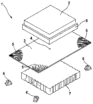
Figure I shows an exemplary diagram of a system according to the invention for
optically imaging an object. The system for optical imaging 1 enables an
object 2 to
be imaged onto a detection device 7 by means of a pinhole aperture 4 which is
integrated into a film mask 3. The object plane is the plane in which the
surface of
the object 2 to be imaged, for example a 2D code, is located and the detection
plane
is the plane in which the imaging plane of the detection device 7 is located.
Both
planes are essentially perpendicular to the optical axis of the system which
runs
from the object 2 perpendicularly through the pinhole aperture 4 to the
detection
device 7. An image of the object 2 is formed on the detection device 7 by
reflection-
optical methods in the preferred embodiment shown. For this purpose the
surface
of the object 2 is illuminated by several illumination devices 6. Optical
attenuation
elements 5 which in the case shown are designed as aperture structures that
are
alternately substantially transparent and substantially impermeable to light
are
located according to the invention between the individual illumination devices
6
and the object 2 to be illuminated. In the preferred embodiment shown the
optical
attenuation elements 5 are also integrated into the film mask 3. The optical
attenuation elements 5 change the illumination of the object 2 by the
illumination
devices 6 in such a manner that the central areas of the object 2 are
illuminated at a
lower light intensity than the peripheral areas of the object 2. An optical
system
window 8 is also shown in figure 1. This is located between the film mask 3
and the
CA 02595354 2007-07-19
WO 2006/077105 PCT/EP2006/000424
-25-
object 2 to be imaged and can be used to border and define the image section
and to
define the distance between object 2 and pinhole aperture 4.
Figure 2 shows an exemplary embodiment of a film mask according to the
invention. The film mask 3 can preferably be produced by light exposure using
an
appropriate template mask and subsequent development of a light-sensitive film
material. In the preferred embodiment shown the optical attenuation elements 5
which in this case are in the form of aperture structures and also the pinhole
aperture 4 are integrated into the film mask. In the case shown four aperture
structures located at different positions are applied which each lie in front
of an
illuminating light source. If several illumination sources are used as in this
case to
illuminate the object, it is advantageous to design the individual aperture
structures
such that the central areas of the object are illuminated with a lower light
intensity
than the peripheral areas of the object due to superimposition of the light
intensities
of the individual light sources in the object plane. In order to facilitate
the
positioning of the film mask in the optical system, additional punch marks 9
are
applied in the embodiment shown. In order to facilitate an unequivocal
identification and characterization of the film mask, additional film marks 10
are
applied in the embodiment shown. These can be exposed on the film together
with
the pinhole aperture and aperture structures and ca ii fi-i, example carry
information
about the shape and size of the pinhole aperture or the shape and the
attenuation
properties of the aperture structures.
Figure 3 shows a detailed view of an exemplary embodiment of an aperture
structure.
The figure shows a special embodiment of an aperture structure 11 which was
exposed to light on a film mask 3. Such an aperture structure can be used
according
to the invention as optical attenuation elements 5. In the embodiment shown
the
aperture structure consists of concentric lines of low transmission (dark
areas) and
intermediate areas of high transmission (light areas) whose widths and
distances
from one another are designed such that the central areas of the object are
illuminated at a lower light intensity than the peripheral areas of the
object. This
CA 02595354 2007-07-19
WO 2006/077105 PCT/EP2006/000424
-26-
special embodiment is particularly suitable for the inventive illumination of
an
object with light sources arranged obliquely to the optical axis. The dark,
light-
impermeable areas in the left upper area of the aperture structure are in this
case
directly below the light source and prevent other areas than those near to the
object
from being illuminated to avoid an indirect scattered light illumination. In
the
present case the object to be illuminated would be at the bottom on the right.
The
high ratio of light-impermeable areas to light-permeable areas in the centre
of the
aperture structure in this case results in a relatively low light intensity in
the centre
of the object; the decreasing ratio of light-impermeable areas to light-
permeable
areas of the aperture structure towards the periphery results in this case in
an
increasingly stronger light intensity towards the periphery of the object thus
enabling the object to be illuminated according to the invention.
Figure 4 shows a view of a system according to the invention for recording and
processing optical information which can for example be integrated into a
diagnostic test element analytical system.
Figure 4a shows a schematic exploded view of such,a system which can be used
as a
component of a diagnostic test element analytical system to record and process
information which is stored on the test element.
The system shown contains a test strip holder 13 into which the test element
12
which in this case is in the form of a test strip can be inserted and which
serves as a
guide and holder for the test element 12. One end of the test element 12
contains
the object 2 which is to be imaged by the system which in this case is in the
form of
a two-dimensional code on the test element 12. The test strip holder 13 is
attached
to a base plate 15 which can anchor the system in the analytical instrument.
In the
embodiment shown the test element holder 13 is designed such that the area
around
the object to be imaged is formed as a so-called strip aperture 17 which
defines the
area of the object to be imaged. A film mask 3 is located above the object 2
to be
imaged which carries a pinhole aperture and the optical attenuation elements
that
are preferably aperture structures. This film mask 3 is mounted on a holder 14
in
such a manner that there is a defined spacing between the pinhole aperture and
the
CA 02595354 2007-07-19
WO 2006/077105 PCT/EP2006/000424
-27-
object plane. A film pressing means 20 is located above the film mask 3 which
on
the one hand, additionally fixes the film mask 3 and, on the other hand,
defines a
defined distance between the film mask 3 and the detection plane so that
reproducible and defined imaging properties can be achieved. Also the
enlargement
scale can be defined by the width of the film pressing means 20 and adapted to
the
respective sensor. The illumination and detection unit 16 is located above the
film
pressing means which in this case is only shown schematically for the sake of
better
clarity. This is positioned by the holder 14 in a defined position relative to
the film
mask 3 and to the object plane.
Figure 4b shows a detailed diagram of this illumination and detection unit 16
which
in this case is shown from the underside for perspective reasons. The
illumination
and detection unit 16 has a detection device 7 which in this case is
preferably in the
form of a CMOS sensor. This detection device 7 is mounted in a housing 21. In
order to protect the detection device 7 against damage, a transparent cover 18
can
be optionally placed in front of it. The evaluation devices of the system can
as in the
example shown of the CMOS sensor, be integrated into it but also be present as
separate components and circuits. The connection 19 with which this unit can
be
connected to the remaining information processing system of the evaluation
device
is used in this case to supply power to the illumination and detection unit 16
and
for data transfer. In the present case the illumination device 6 is composed
of four
individual LEDs which are obliquely arranged relative to the optical axis of
the
imaging system. Such oblique arrangements of the illumination sources are
especially advantageous when importance is attached to the smallest possible
constructional depth of the imaging system.
Figure 5 shows images of different surfaces recorded by a CMOS sensor which
were
recorded by an optical system according to the invention containing
appropriate
aperture structures as optical attenuation elements. The first column of
figure 5
shows in each case the image of the film mask used in each case with the
corresponding aperture structures, the second column shows the image of a mat
polyester surface (Melinex PET polyester film, DuPont) recorded by a CMOS
sensor and the third column shows the image of a glossy photopaper recorded by
a
CA 02595354 2007-07-19
WO 2006/077105 PCT/EP2006/000424
-25-
CMOS sensor. Such homogeneous and in particular uniformly structured and
uniformly coloured surfaces can be used to gain information about the system-
inherent brightness distribution in the detection plane. Such a brightness
distribution enables information to be obtained on the system-inherent imaging
properties of the optical system.
In each case film masks are used which have 4 aperture structures each
consisting of
concentric circles of low transmission (dark areas) and intermediate areas of
high
transmission (light areas) where the ratio of light-impermeable areas to light-
permeable areas decreases towards the periphery of the respective aperture
structure. In order to improve the illumination situation, the part of the
aperture
structure located below the light source is additionally darkened.
Figure 5a) shows a film mask in which a light-permeable area is additionally
arranged around the aperture structure comprising concentric lines. The CMOS
recordings of homogeneous surfaces using such film masks show an essentially
cross-shape structure with light areas between the illumination devices and
dark
areas in the corners.
Figure 5b) shows a film mask that is similar to 5a) in which the part of the
aperture
structure located below the illumination device has been reduced in size. The
CMOS recordings of homogeneous surfaces using such film masks also show an
essentially cross-like structure in which the light areas are more extensive
compared
to 5a).
Figure 5c) shows a film mask in which no additional light-permeable area is
present
around the aperture structure consisting of concentric lines but rather this
area is
light-impermeable. The part of the aperture structure located below the
illumination device is again arranged centrally. The CMOS recordings using
such
aperture structures show a much more uniform brightness distribution in the
detection plane. Such an aperture structure according to the invention enables
the
object to be imaged in the detection plane essentially free of system-inherent
CA 02595354 2007-07-19
WO 2006/077105 PCT/EP2006/000424
-29-
imaging defects and can thus be the basis for reliable information transfer
that is as
free of errors as possible.