Note: Descriptions are shown in the official language in which they were submitted.
CA 02595719 2007-08-15
DEMANDES OU BREVETS VOLUMINEUX
LA PRPESENTE PARTIE DE CETTE DEMANDE OU CE BREVETS
COMPREND PLUS D'UN TOME.
CECI EST LE TOME DE _2
NOTE: Pour les tomes additionels, veillez contacter le Bureau Canadien des
Brevets.
JUMBO APPLICATIONS / PATENTS
THIS SECTION OF THE APPLICATION / PATENT CONTAINS MORE
THAN ONE VOLUME.
THIS IS VOLUME OF _2
NOTE: For additional volumes please contact the Canadian Patent Office.
CA 02595719 2007-08-15
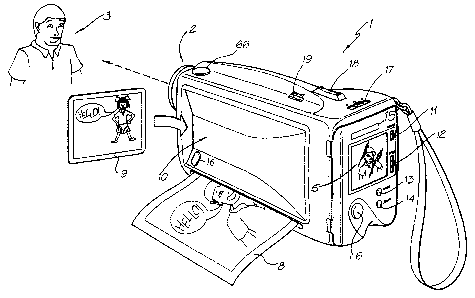
IMAGE TRANSFORMATION MEANS INCLUDING USER INTERFACE
Field of the Invention
The present invention relates to an image processing method and apparatus and,
in particular, discloses a
Digital lnstant Camera with Image Processing Capability.
The present invention further relates to the field of digital camera
technology and, particularly, discloses a
digital camera having an integtal color printer.
Backpõt outtd of the lnvention
Traditional camera technology has for many years relied upon the provision of
an optical processing system
which relies on a negative of an image which is projected onto a
photosensitive film which is subsequently
chemically processed so as to "fix" the fiim and to allow for positive prints
to be produced which reproduce the
original image. Such an image processing technology, although it has become a
standard, can be unduly complex, as
expensive and difficult technologies are involved in full color processing of
images. Recently, digital cameras have
become available. These cameras nonmally rely upon the utiliration of a
charged coupled device (CCD) to sense a
particular image. The camera normally includes storage media for the storage
of the sensed scenes in addition to a
connector for the transfer of images to a computer device for subsequent
manipulation and printing out.
Such devices are generally inconvenient in that ali images must be stored by
the camera and printed out at
some later stage. Hence, the camera must have sufficient storage capabilities
for the storing of multiple images and,
additioinally, the user of the camera must have access to a subsequent
computer system for the downloading of the
images and printing out by a computer printer or the like.
Further, PolaroidTm type instant cameras have been available for some time
which allow for the production
of instant images. However, this type of camera has limited utility producing
only limited sized images and many
problems exist with the chemicals utilised and, in particular, in the aging of
photographs produced from these types of
cameras.
When using such devices and other image capture devices it will be desirable
to be able to suitably deal
with audio and other environmentai information when taking a picture.
Further, the creation of stereoscopic views, with a first image being
presented to the left eye and second
image being Presented to the right eye, thereby cresting an illusion of a
three dimensional surface is well known.
However, previous systems have required complex preparation and high fidelity
images have generally not been
possible. Further, the general choice of images has been limited with the
images normally only being specially
prepared images.
There is a general need for being able to produce high fidelity stereoscopic
images on demand and in
particular for producing images by means of a portable camera device wherein
the stereoscopic image can be
taken at will.
Further, it would be highly convenient if such a camera picture image
production system was able to create
automatic customised postcatds which, on a fust surfaee contained the image
captured by the camera device and, on a
second surface, contains pre-paid postage marks and address details.
Recetttly, it has become more and more popular in respect of photographic
reproduction techniques to
produce longer and longer "panoramic views of a image. These images can be
produced on photographic paper or
CA 02595719 2007-08-15
-2-
the iike and the strucn,re of the image is normally to have longer and longer
lengths in comparison to the width so as
to produce the more "panoramic" type views. Unfortunately, this imposes a
problem where the photographic paper to
be imaged upon originally was stored on a roll of small diameter.
Recently, it has become quite popular to provide filters which produce effects
on images similar to popular
artistic painting styles. These filters are designed to take an image and
produce a resultant secondary image which
appears to be an artistic rendition of the primary image in one of the
aetistic styles. One extremely popular artist in
modem times was Vincent van Gogh. It is a characteristic of art works produced
by this artist that the direction of
brush strokes in flat areas of his paintings strongly follow the direction of
edges of dominant features in the painting.
For example, his works entitled "Road with Cypress and Star", "Starry Night"
and "Portrait of Doctor Gachet" are
illustrative examples of this process_ It would be desirable to provide a
computer algorithm which can automatically
produce a"van Gogh" effect on an arbitrary input image an output it on a
portable camera system..
Unfortunately, warping systems generally utilised high end computers and are
generaily inconvenient in that
an image must be scanned into the computer processed and then printed out.
This is generally inconvenient,
especially where images are captured utilising a hand held camera or the like
as there is a need to, at a later stage,
transfer the captured images to a computer system for manipulation and to
subsequently manipulate them in
accordance with requirements.
Further, new and unusual effects which simulate various painting styles are
often considered to be of great
value. Further, if these effects can be combined into one simple form of
implementation they would be suitable for
incorporation into a portable camera device including digital imaging
capabilities and thereby able to produce desire
filtetrd images of scenes taken by a camera device.
Unfortunately, changing digital imaging bechnologies and changing filter
technologies result in onerous
system requirements itt that cameras produced today obviously are unable to
take advantages of technologies not yet
available nor are they able to take advantage of filters which have not, as
yet, been created or conceived.
One extremely popular form of carttera technology is the tradidonal negative
film and positive print
photographs. In this case, a camem is utilized to image a scene onto a
negative which is then processed so as to fix
the negative. Subsequently, a set of prints is made from the negative. Further
sets of prints can be instantly created at
any time from the set of negatives. The prints normally having a resolution
close to that of the original set of prints.
Unfortunately, with digital camera devices, including those proposed by the
present applicant, it would be necessary
to permanently store in a digital fona the photograph capntred and printed out
if ftuther copies of the image were
desired at a later time. Ihis would be generally inconvenient in that,
ideally, a copy of a"photograph" should merely
require the initial print. Of course, altematively, the original print may be
copied utilising a high quality colour
photooopying device. Unfortunately, any such device has limited copy
capabilities and signal degradation will often
be the result when such a form of copying is used. Obviously, more suitable
forms of producing copies of camera
prints are desirable.
Further, Ahnost any artistic painting of a scene utilises a restricted gamut
in that the artist is limited in the
colours produced as a result of the choice of medium in rendering the image.
This restriction is itself often
exploit,ed by the artist to produce various artistic effects. Classic examples
of this process include the following
well known artistic works:
CA 02595719 2007-08-15
-3-
- Camille Pissaro' L'le Lacroix - Rouen, effect de brouillard" 1888. Museum of
Art,
Philadeiphie
- Charles Angrand "Le Seine - L'aube" - 1889
collection du Petit Palais, Geneve
- Henri van de Velde "Crepuscule" - 1892. Rijksmuseum KrSller MQller, Otterlo
- Georges Seurat. "La cote du Bas-Butin, Honfieur" 1886 - Muse des Beaux -
Arts, Toumai
It would be desirable to produce, from an arbitrary input image, an output
image having similar effects or
characteristics to those in the above iist.
A number of creative judgements are made when any garment is created. Firstly,
there is the shape and
styling of the garment and additionally, there is the fabric colours and
style. Often, a fashion designer will try
many different altematives and may even attempt to draw the final fashion
product before creating the fmished
garment.
Such a process is generally unsatisfactory in providing a rapid and flexible
tum around of the garments and
also providing rapid opportunities judgement of the final appearance of a
fashion product on a person.
A number of creative judgements are made when any garment is created. Firstly,
there is the shape and
styling of the garment and additionally, there is the fabric colours and
style. Often, a fashion designer will try
many different alternatives and may even attempt to draw the fmal fashion
product before creating the finished
garment.
Such a process is generally unsatisfactory in providing a rapid and flexible
turn around of the garments and
also providing rapid judgement of the final appearance of a fashion product on
a person.
Binocular and telescope devices are well known. In particular, taking the
example of a binocular device,
the device provides for telescopic magnification of a scene so as to enhance
the user's visual capabilities_ Further,
devices such as night glasses etc. also operate to enhance the user's visual
system. Unfortunately, these systems
tend to rely upon real time analog optical components and a permanent record
of the viewed scene is difficult to
achieve. One methodology perhaps suitable for recording a permanent copy of a
scene is to attach a sensor device
such as a CCD or the like so as to catch the scene and store it on a storage
device for later printing out.
Unfortunately, such an arrangement can be unduly cumbersome especially where
it is desired to utilize the
binocular system in the field in a highly portable manner.
Many forms of condensed information storage are well known. For example, in
the field of computer
devices, it is common to utilize magnetic disc drives which can be of a fixed
or portable nature. In respect of
portable discs, "Floppy Discs", "Zip Dises", and other fotms of portable
magnetic storage media have to achieve
to date a large degree of acceptance in the market place. Another form of
portable storage is the compact disc
"CD" which utilizes a series of elongated pits along a spiral track which is
read by a laser beam device. The
utilization of CD's provides for an extremely low cost form of storage.
However, the technologies involved are
quite complex and the use of rewritable CD type devices is extremely limited
Other forms of storage include magnetic cards, oRen utilized for credit cards
or the like. These cards
normally have a magnetic strip on the back for recording information which is
of relevance to the card user.
Recently, the convenience of magnetic cards has been extended in the form of
SmartCard technology which includes
CA 02595719 2007-08-15
-4-
incotponition of integrated circuit type devices on to the card.
Unfortunately, the cost of such devices is often high
and the ootnplexity of the technology utilized can also be sigaificant
Traditionalty silver halide camera processing systems have given rise to the
well known utilisation of a
"negative" for the production of multiple prints. The negative normally fotnis
the source of the production prints and
the pntctice has grown up for the independent care and ptotection of negatives
for their subsequent continual
utilisation.
With any form of encoding system which is to be sawed in a fault tolerant
manner, there is the significant
question of how best to encode the data so that it can be effoctively and
efficiently decoded- It is the.refore desirable
to provide for an effective encoding sysiein.
Summary of the Invention
A user interface for operating a device, said user interface comprising a card
which is inserted in a
machine and on the face of the card is contained a visual representation of
the effect the card will have on
the output of the machine.
Further aspects disclosed herein include:
An alternative form of camera system which includes a digital camera with an
integral color
printer. Additionally, the camera provides hardware and software for the
increasing of the apparent
resolution of the image sensing system and the conversion of the image to a
wide range of "artistic styles"
and a graphic enhancement.
In acondance with afinthQ of the
asped presatt invention, there is provided a catnera system canprising at
least one area itoage sensor for imaging a soene, acunem processor means for
processing said imaged scene in
accordance with a predetermined scene transformation requitnment, a printer
for priating out said processed
image
sceue on print medis, print media and printing ink stored in a single
detachable module inside said catneta system,
said camera system comprising a portable hand held unit for the imaging of
scenes by said area image sensor aag
prklttng said soenes dneWy out of said camera system via said printa.
Preferably the camera system ineludes a print roll for the storage of print
media and priniing ink for
utilization by the printer, the print roll being detachabie from the camera
system. Further, the print noU can inchtde an
authentication chip containing authentication infonnation and the camera
processing meaas is adapted to interrogate
the authentication chip so as to detenmine the authenticity of said print roU
when insarted wititin said camera system_
Further, the
, printu can include a drop on demand ink printa and guittotitm means for the
separation of
Irinted Pltotogniphs.
In accordance with a first aspect of the present invention, there is provided
a camnera system comprising at
lad one atea image sensor for imag6tg a scaie, = a camera processor means for
prooessiog said image scene in
aocordance with a predetermined scene transfonnation requirement, a printer
for printing out said processed image
sceae on print media said prv-ter, print media and printing ink stored in a
single dotachable moduk inside said cameca
systtm, said carneta system comprising a pottable hand held unit for the
imaging of scenes by said area image sensor
and p-inting said scenes directly out of said camera system via said prilger
T'refaablY the camaa system includes a print roU for the storage of print
media and printing ink for
utt7isatiot- by the ptinter, s the aid print roll being detachable from the
camera systan. i=lather, the print roU can
include an authentication chip containing autheatication information and the
camera processing means is adapted to
'nftn 8aft the authentcafion chip so as to detamine the authenticity of said
print roll when iaserted within said
camera system.
Further, the printer can include a drop on demand ink printer and guillotine
means for the separa<ion of
CA 02595719 2007-08-15
-5-
psu-ted photographs.
In aesowdance with a further aspect of the invention there is provided the
camera system comprnsing:
at least one area inune sensor for imaging a scene;
a camera processor means for processing said imaged scene in accordance with a
predetetmined scene
ttmsformation requimnent;
a printer for printing out said processed image scene on print media said
printer,
a detachable moduk for storing said print media and printing ink for said
printer,
said camera system comprising a portable hand held unit for the imaging of
scenes by said area iinage sensor
and printing said scenes directly out of said camera system via said printer.
In accordance with a further aspect of the present invention, there is
provided a camera system
cotnprising a sensor means for sensing an image; a processing means for
processing the sensed image in
accordance with a predetermined processing requirement, if any; audio
recording means for according an audio
signal to be associated with the sensed image; printer means for printing the
processed sensed image on a first area
of a print media supplied with the camaa system, in addition to printing an
encoded version of the audio signal on
a second area of the print media. Preferably the sensed image is printed on a
first surface of the print media and
the encoded version of the audio signal is printed on a second surface of the
print media.
In accordance with the present invention thete is provided a camera system
having:
an area image sensor means for sensing an image;
an image storage means for storing the sense image;
an orientation means for sensing the cameta's orientation when sensing the
image; and
a processing means for processing said sensed image utilising said sensed
cxmera orientation.
In accordance with the present invention thene is provided a camera systean
having:
an area image sensor means for sensing an image;
an image storaga means for storing the sense image;
an orientation means for sensing the cameta's ocientation when sensing the
image; and
a prooessing means for processing said sensed image utilising said sensed
camera orleattation.
In accordance with a further aspect of the present invention there is provided
a method of processing a digital
image comprising:
captnring the image utilising an adjustable focusing technique;
utilising the focusing settings as an indicator of the position of strucnu-es
within the image;
processing the image, utilising the said focus settings to produce effeets
specific to said focus settings; and
printing out the itnage.
Pttiferably the image can be eapturzd utilising a zooming technique; and the
z,ooming settings can be used in a
hearistic manner so as to process portions of said image.
CA 02595719 2007-08-15
-6-
In accordance with a further aspect of the invention there is provided a
method of processing an image taken
with a digital camera including an eye position sensing means said method
comprising the step of utilizing the eye
position information within the sensed image to process the image in a
spatially varying sense, depending upon said
location information.
The utilizing step can comprise utilizing the eye position information to
locate an area of interest within
said sensed image. The processing can includes the placement of speech bubbles
within said image or applying a
region specific warp to said image. Aitetttatively the processing can include
appiying a brush stroke filter to the
image having greater detail in the area of said eye position information.
Ideally the camera is able to substantially
immediately print out the rosulu of the processing.
In accordance with a further aspect of the invention there is provided a
method of processing an image taken
with a digital camera including an auto exposure setting, said method
comprising the step of utilising said information
to process a sensed image.
The utilising step can comprise utilising the auto exposure setting to
determine an advantageous rermapping
of colours within the image so as to produce an amended image having colours
within an image iransformed to
account of the auto exposure setting. The processing can comprise re-mapping
image colours so they appear deeper
and richer when the exposure setting indicates low light conditions and re-
mapping image colours to be brighter and
more saturated when the auto exposure setting indicates bright light
conditions.
The utilising step includes adding exposure specific graphics or manipulations
to the image.
Recently, digital cameras have become inaeasingly popular. Ihese cameras
normally operate by means of
imaging a desired image utilising a charge coupled device (CCD) array and
storing the imaged scene on an electronic
stonige medium for later down loading onto a computer system for subsequent
manipulation and printing out.
Normally, when utilising a computer system to print out an image,
sophisticated software may available to manipulate
the image in accordance with requiremems.
Utifortunately such systems require significant post processing of a captured
image and normally present the
image in an orientation to which is was taken, relying on the post processing
process to perform any necessary or
required modifications of the captured image. Further, much of the
environmental information available when the
picdue was taken is lost.
Recently, digital c.ameras have become increasingly popular. These catneras
normally operate by means of
imaging a desired image utilising a charge coupled device (CCD) atray and
storing the imaged scene on an elecironic
storage medium for later down loading onto a computer system for subsequent
manipulation and printing out.
Normally, when utilising a computer system to print out an image,
sophisticated software may available to manipulate
the image in accordanoe with requ'veinents.
Unfortunately such systems tr,quire signifioant post processing of a capturad
image and nomtally present the
image in an orient,ation to which is was taken, relying on the post processing
pnooess to perform any necessary or
required modifications of the captured image. Further, much of the
enviraunental information available when the
pieture was taken is lost.
In accordance with a 5uther aspect of the present invention there is provided
a method of processing an
image captured utilising a digital camera and a flash said method comprising
the steps of :
CA 02595719 2007-08-15
-7-
a) locating distortions of said caphued image due to the utilisation of said
flash;
b) retouching said image so as to locally reduce the effect of said
distortions.
In accordance with the second aspect of the present invention there is
provided a digital camera having
reduced flash distortion effects on captured images comprising;
(a) a digital means capturing image for the capture of images;
(b) a distortion location means for locating flash induced colour distortions
in the captured
image; and
(c) image inversed distortion means connected to said distortion location
means and said
digital image capture means and adapted to process said captured image to
reduce the effects of said distortions;
(d) display means connected to said distortion for displaying.
In accordance with a further aspect of the present invention there is provided
a method of creating a
stereoscopic photographic image comprising:
(a) utilising a camera device to image a scene stereographicaily;
(b) printing said stereographic image as an integrally formed image at
predetermined positions on a
first surface portion of a transparent printing media, said transparent
printing media having a second surface
including a lensing system so as to stereographically image said scene to the
left and right eye of a viewer of said
printed stereographic image.
In accordance with a further aspect of the present invention there is provided
a print media and ink supply
means adapted to supply a printing mechanism with ink and printing media upon
which the ink is to be deposited,
said media and ink supply means including a roll of media rolled upon a media
former within said media and ink
suppiy means and at least one ink reservoir integrally formed within said
media and ink supply means and adapted to
be connected to said printing mechanism for the supply of ink and printing
media to said printing mechanism.
In accordance with a further aspect of the present invention there is provided
a print media and ink supply
means adapted to supply a printing mechanism with ink and printing media upon
which the ink is to be deposited,
said media and ink supply means including a roll of media rolled upon a media
fom-er within said media and ink
supply means and at least one ink reservoir integrally formed within said
media and ink supply means and adapted to
be connected to said printing mechanism for the supply of ink and printing
media to said printing mechanism.
In accordance with a further aspect of the present invention then: is provided
a print roll for use in a camera
imagirtg system said priat roll having a backing surface having a plurality of
formatted postcard infonnation printed
at pre-determined intervals.
In accordance with the second aspect of the present invention there is
provided a method of creating
customised postcards comprising the steps oF utilising a camera device having
a print roll having a backing surface
including a pluraiity of formatted postcard infonmation sections at pre-
determined positions on said backing surface;
imaging a customised image on a corresponding intaging surface of said print
roll; and
utilising said print roll to produce postcards via said camera device.
In accordance with the third aspect of the present invention there is provided
a method of sending
postcards comprising cxmera images through the postal system said method
comprising steps of
setting a print roll having prepaid postage contained within the print roll;
CA 02595719 2007-08-15
-8-
utilising the print roll in a camera unaging system to produce postcards
having prepaid postage; and
sending said prepaid postcards through the mail.
The present invention is further directed to a caaznera system with an
integral printer type device. The print
media being detachable from the camera system and including a means for the
storage of significant infonnation in
respect of the print media.
Ilie present invention is further directed to a camera system with an integral
printer type device. The print
media being detachable from the camera system and including means for
providing an authentication access to the
print media.
In accordance with a further aspect of the present invention there is provided
a plane print media having a
reduced degree of curling in use, said print media having anisotropic
stifihess in the direction of said planes.
In accordance with the second aspect of the present invention there is
provided a method of reducing the curl in an
image printed on plane print media having an anisotropic stiffness said method
comprising applying a localised
pressure to a portion of said print media.
The present invention is further directed to a camera system with an integral
printer type device. The camera
systetn including an indicator for the number of images left in the printer,
with the indicator able to display the
number of prints left in a number of different modes.
In accordance with a further aspect of the present invention there is provided
a method of automatically
processing an image comprising locating within the image features having a
high spatial variance and stroking the
image with a series of brush strokes emanating from those areas having high
spatial variance. Preferably, the
bnLsh strokes have decreasing sizes near impottant features of the image.
Additionally, the position of a
predetermined portion of brust strokes can undergo random jitterittg.
In accordance with a further aspect of the invention there is provided a
method of warping of producing a
warped image from an input image, said method comprising the steps of:
inputting a warp map for an arbitrary output image having predetennined
dimensions A x B, each element of
said warp map mapping a corresponding region in a theoretical input image to a
pixel location of said arbitrary output
image corrcsponding to the co-ordinate location of said element within said
warp map;
soaling said warp map to the ditnensioas of said warped image so as to produce
a scaled warp map;
for substantially each element in said sealed warp map, calcalating a
contribution region in said input image
through utiliztion of said element value and adjacent element values; and
determining an output image colour for a pixel of said warped image
corresponding to said element &om
said contribution region.
In accordatnce with a further aspect of the present invention, there is
provided a method of increasing the
resilience of data stored on a medium for reading by a sensor device pricing
the steps of
(a) modulating the stored data in a recoverable fashion with the modulating
signal having a
high frequency component.
(b) storing the data on said medium in a modulated form;
(c) sensing the modulated stored data by said sensor device;
(d) neutralising the modulation of the modulated stoned data to track the
spread of location of
CA 02595719 2007-08-15
-9-
said modulated stored data on said medium; and
(e) recovering the unmodulated stored data from the modulated stored data.
The preferred embodiment of the present invention will be described with
reference to a card reading system
for reading data via a CCD type device into a camera system for subsequent
decoding. Further, the discussion of the
preferred embodiment relies heavily upon the field of error control systems.
Hence, the person to which this
specification is directed should be an expert in error of control systems and
in particular, be fvmly familiar with such
standard texts such as "Error control systems for Digital Communication and
Storage" by Stephen B Wicker
published 1995 by Prentice - Hall Inc. and in particular, the discussion of
Reed - Solomon codes contained therein
and in other standard text.
It is an object of the present invention to provide for a method of converting
a scanned image comprising
scanned pixels to a coiresponding bitmap image, said method comprising the
steps of, for each bit in the bitmap
image;
a. determining an expected location in said scanned image of a current bit
from the location of
surrounding bits in said scamied image;
b. detennining a likely value of said bit from the values at the locations of
expected corresponding
pixels in said scanned image;
c. determining a centroid measures of the centre of the centre of the expected
intensity at the said
expected location;
d. determining similar centroid measures for adjacent pixels surrounding said
current bit in said
scanned image and;
e. where said centroid measure is improved relative to said expected location,
adjusting said expected
location to be an adjacent pixel having an improved centroid measure.
In accordance with a further aspect of the present invention there is provided
an apparatus for text editing
an image comprising a digital camera device able to sense an image; a
manipulation data entry card adapted to be
inserted into said digital camera device and to provide manipulation
instructions to said digital camera device for
manipulating said image, said manipulation instructions including the addition
of text to said image; a text entry
device connected to said digital camera device for the entry of said text for
addition to said image wherein said
text entry device includes a series of non-roman font characters utilised by
said digital camera device in
conjunction with said manipulation instructions so as to create new text
characters for addition to said image.
Preferably, the font characters are transmitted to said digital camera device
when required and rendered
by said apparatus in accordance with said manipulation instructions so as to
create said new text characters. The
manipulation data entry card can include a rendered roman font character set
and the non-roman characters
include at least one of Hebrew, Cyrillic, Arabic, Kanji or Chinese characters.
In accordance with a further aspect of the present invention there is provided
an apparatus for text editing
an image comprising a digital camera device able to sense an image; a
manipulation data entry card adapted to be
inserted into said digital camera device and to provide manipulation
instructions to said digital camera device for
manipulating said image, said manipulation instructions including the addition
of text to said image; a text entry
device connected to said digital camera device for the entry of said text for
addition to said image wherein said
CA 02595719 2007-08-15
-10-
text entry device includes a series of non-roman font characters utilised by
said digital camera device in
conjunction with said manipulation instructions so as to create new text
characters for addition to said image.
Preferably, the font characters are transmitted to said digital camera device
when required and rendered
by said apparatus in accordance with said manipuiation instructions so as to
create said new text characters. The
manipulation data entry card can include a rendered roman font character set
and the non-roman characters
include at least one of Hebrew, Cyrillic, Arabic, Kanji or Chinese eharacters.
It is an object of the present invention to provide a systern which readily is
able to take advantage of updated
technologies in a addition to taking advantage of new filters being ctrated
and, in addition, providing a readily
adaptable form of image processing of digitally captured images for printing
aut. _.-
In accordance with a further aspect of the present invention, there is
provided an image copying device for
reproduction of an input image which comprises a series of ink dots, said
device comprising:
(a) imaging array means for imaging said input image at a sampling rate higher
than the frequency of
said dots so as to produce a corresponding sampled image;
(b) processing means for processing said image so as to determine the location
of said print dots in said
sample image;
(c) print means for printing ink dots on print media at locations
corresponding to the locations of said
print dots.
2. An image copying device as claimed in claim 1 wherein said copying device
prints a full color
copies of said input image.
In accordance with a further aspect of the present invention there is provided
a camera system for
outputting deblurred images, said system comprising;
an image sensor for sensing an image; a velocity detection means for
determining any motion of
said image relative to an externai environment and to produce a velocity
output indicative thereof; a processor
means interconnected to said image sensor and said velocity detection means
and adapted to process said sensed
image utilising the velocity output so as to deblurr said image and to output
said deblurred image.
Preferably, the camera system is connected to a printer means for immediate
output of said deblurred
image and is a portable handheld unit. The velocity detection means can
comprise an accelerometer such as a
micro-electro mechanical(IvEMS) device.
In accordance with a fiulher aspect of the present invention, there is
provided a photosensor reader preform
oomprising:
(a) a series of light emitter recesses for the insettion of light emitted
devices;
(b) light emitter focusing means for focusing light emitted from the series of
light emitter devices onto
the surface of an object to be intaged as it traverses the surface of said
pn;fornn;
(c) a photosensor recess for the inseition of a linear photosensor array; and
(d) focussing means for focussing light reflected frotn said object to be
unaged onto a distinct portion
of said CCD array.
In accordance with an aspect of the present invention, there is provided a
printer device for
interconnection with a computer system comprising a printer head unit
including an ink jet print head for printing
CA 02595719 2007-08-15
_ 11_
images on print media and further having a cavity therein for insertion of a
consumable print roll unit and a print
roll unit containing a consumable print media and ink for insertion into said
cavity, said ink being utilised by said
ink jet print head for printing images on said print media.
In accordance with a further aspect of the present invention, there is
provided a digital camera system
comprising a sensing means for sensing an image; modification means for
modifying the sensed image in
accordance with modification instructions input into the camera; and an output
means for outputting the modified
image; wherein the modification means includes a series of processing elements
arranged around a central
crossbar switch. Preferably, the processing elements include an Arithmetic
Logic Unit (ALU) acting under the
control of a microcode store wherein the microcode store comprises a writeable
control store. The processing
elements can include an internal input and output FIFO for storing pixel data
utilized by the processing elements
and the modification means is interconnected to a read and write FIFO for
reading and writing pixel data of
images to the modification means.
Each of the processing elements can be arranged in a ring and each element is
also separately connected
to its nearest neighbours. The ALU accepts a series of inputs interconnected
via an internal crossbar switch to a
series of core processing units within the ALU and includes a number of
internal registers for the storage of
temporary data. The core processing units can include at least one one of a
muttiplier, an adder and a barrel
shifter. .
The processing elements are further connected to a common data bus for the
transfer of pixel data to the
processing elements and the data bus is interconnected to a data cache which
acts as an intennediate cache between
the processing elements and a memory store for storing the images.
In accordance with a further aspect of the present invention there is provided
a method of rapidiy
decoding, in real time, sensed image data stored at a high pitch rate on a
card, said method comprising the steps
of;
detecting the initial position of said image data;
decoding the image data so as to determine a corresponding bit pattern of said
image data.
In accordance with a further aspect of the present invention there is provided
a method of rapidly
decoding sensed image data in a fault tolerant manner, said data stored at a
high pitch rate oti a card and subject to
rotations, warping and marking, said mehtod comprising the steps of:
detennining an initial location ofa start of said image data;
sensing said image data at a sampling rate greater than said pitch rate;
processing said sensed image data in a column by column process, keeping an
expected location of the
center of each dot (centroid) of a next cohunn and utilising fme adjustments
of said centroid when processing each
column so as to update the location of an expected next cetttroid.
In accordance with a further aspect of the present invention there is provided
a method of accurately
detecting the value of a dot of sensed image data, said image data comprising
an array of dots and said sensed image
data comprising a sampling of said image data at a rato greater dian the pitch
fieqttency of said array of dots so as to
producx an atray of pixeLs, said method cotnprising the steps of
determining an expected middle pixel of said array of pixels, said middle
pixel corresponding to an expected
CA 02595719 2007-08-15
central location of a corresponding dot;
utilising the sensed value of said middle pixel and the sensed value of a
number of adjacent pixels as an
index to a lookup table having an output corresponding to the value of a dot
centred around the corresponding
location of said pixel.
In accordance with a further aspect of the present invention there is provided
a method of accurately
determining the location of dots of sensed image data amongst an array of dots
of image data in a fault tolerant
manner, said data stored at a high pitch rate on a card and subject to
rotations, warping and marking effects, said
method comprising the steps of:
prooessing the image data in a column by column format;
recording the dot pattern of previously processed columns of pixels;
genetating an expected dot pattern at a cutrent column position from the
recorded dot pattern of previously
processed pixels;
comparing the expected dot pattern with an actual dot pattem of sensed image
data at said current column
position;
if said comparison produces a match within a predetermined error, utilising
said current column position as
an aciual dot position otherwise altering said current column position to
produce a better fit to said expected dot
pattern to thereby produce new aetuai dot position, and
utilising said actual dot position of the dot at a cun~ent column position in
the detamining of dot location of
dots of subsequent columns.
In accordance with a further aspect of the present invention there is provided
a method of combining
image bump maps to simulate the effect of painting on an image, the method
comprising:
defming an image canvas bump map approximating the surface to be painted on;
deftning a painting bump map of a painting object to be painted on said
surface;
combining said image canvas bump map and said painting bump map to produce a
final
composited bump map utilising a stiffness factor, said stiffness factor
determining the degree of modulation of
said painting bump map by said image canvas bump map.
In accordance with a fitrther aspect of the present invention there is
provided =a method of automatically
manipulating an input image to produce an artistic effect comprising:
predetermining a mapping of an input gamut to a desired output gamut so as to
produce a
desired artistic effect;
utilising said mapping to map said input image to an output image having a
predetermined
output gamut;
Preferably, the method further comprises the step of post processing the
output image utilising a brush
stroke filter.
Further, preferably the output gamut is formed from mapping a predetemtined
number of input gamut
values to corresponding output colour gamut values and interpolating the
remaining mapping of input gamut
values to output colour gamut values. The intetpolation process can include
utilising a weighted sum ofsaid
mapping of a predetermined number of input gamut values to corresponding
output colour gamut values.
CA 02595719 2007-08-15
-13-
In accordance with the second aspect of the presettt invention there is
provided a method of compressing
an input colour gamut to be within an output colour gamut, said method
comprising the steps of:
determining a zero chrominance value point at a current input colour
intensity;
determining a source distance being the distance from said zero chrominance
value to
the edge of said input colour gamut;
determining a suitable edge of said output colour gamut;
determining a target distance being the distance from said zero chrominance
value to the edge of
said output colour gamut; and
scaling the current input colour intensity by a factor derived from the ratio
of source
distance to target distance;
Preferably said current input colour intensity is further scaled by a factor
dependent on the distance for
said current input colour from said zero chrominance value point.
In accordance with a futtlter aspect of the present invention, there is
provided a handheld camera for the
output of an image sensed by the camera, with the camera including:
sensing means for sensing an image;
tiling means for adding tiling effects to the sensed image to produce a tiled
image; and
display means for displaying the tiled image.
In accordance with a fnrther aspect of the present invention, there is
provided a handheld camera for the
output of an image sensed by the camera, with the camera including:
sensing means for sensing an image;
texture mapping means for adding texturing effects to the sensed image to
produce a texttu-ed image; and
display means for displaying the textured image.
In xcordance with a further aspect of the present invention, there is provided
a handheld camera for the
output of an image sensed by the camera, with the camera including:
sensing means for sensing an image;
lighting means for adding lighting to the sensed itnage to produce an
illuminated image which simulates the
effect of light sources projected at the sensed image; and
display means for displaying the i[luminated image.
In accordance with a further aspect of the present invention there is provided
a garment creation system
comprising:
a series of input tokens for inputting to a camera device for manipulation of
a sensed image for
outputting on a display device depicting a gannent constructed of fabric
having characteristics of said sensed
image;
a camera device adapted to read said input tokens and sense an image and
manipulate said image
in accordance with a read input token so as to produce said output image; and
a display device adapted to display
said output image
In accordance with a further aspect of the present invention there is provided
A garment creation system
comprising:
CA 02595719 2007-08-15
-14-
an expected image creation system including an image sensor device and an
image display device, said
image creation system mapping portions of an arbitrary image sensed by said
image sensor device onto a garment
and outputting on said display device a depiction of said garment;
a garment fabric printer adapted to be interconnected to said image creation
system for printing out
corresponding pieces of said garment including said mapped portions..
In accordance with a further aspect of the present invention as provided a
method of creating a
manipulated image comprising interconnecting a series of camera manipulation
units, each of said camera
manipulation unit applying an image manipulation to an inputted image so as to
produce a manipulated output
image, an initial one of said camera manipulation units sensing an image from
an environment and at least a final
one of said camera manipulation units producing a permanent output image.
In accordance with a further aspect of the present invention there is provided
a portable imaging system
for viewing distant objects comprising an optical lensing system for
magnifying a viewed distant object; a sensing
system for simultaneously sensing said viewed distant object; a processor
means interconnected to said sensing
system for processing said sensed image and forwarding it to a printer
mechanism; and a printer mechanism
connected to said processor means for printing out on print media said sensed
image on demand by said portable
imaging system.
Preferably the system further comprisos a detachable print media supply means
provided in a detachable
module for interconnection with said printer mechanism for the supply of a
roll of print media and ink to said
printer mechanism.
The printer mechanism can comprise an ink jet printing mechanism providing a
full color printer for the
output of sensed images.
Further, the prefemed embodiment is implemented as a system of binoculars with
a beam splitting device
which projects said distant object onto said sensing system.
In accordance with a fiuther aspect of the present invention, there is
provided a system for playing
prerecorded audio encoded in a fault tolerant manner as a series of dots
printed on a card, the system comprising
an optical scanner means for scanning the visual form of the prerecorded
audio; a processor means interconnected
to the optical scanner means for decoding the scanned audio encoding to
produce a corresponding audio signal;
and audio emitter means inter+connected to the processor means for emitting or
playing the corresponding audio
signal on demand.
The encoding can include Reed-Solomon encoding of the pm.recorded audio and
can comprise an array
of ink dots which are high frequency modulated to aid scanning.
The system can include a wand-like arm having a slot through which is inserted
the car.d.
In accordance with a further aspect of the present invention, there is
provided a method of information
distribution on printed cards, the method comprising the steps of dividing the
surface of the card into a number of
predetennined areas; printing a first collection of data to be stored in a
first one of the predetermined areas;
utilising the printed fust predetermined area when reading information stored
on the card; and, when the
informadon stored on the card is to be updated, dotermining a second one of
the predetennined areas to print
further information stored on the card, the second area not having being
previously utilized to print data.
CA 02595719 2007-08-15
-15-
Preferably, the areas are selected in a predetermined order and the printing
utilizes a high resolution ink
dot printer for printing data having a degree of fault tolerance with the
fault tolerance, for example, coming from
Reed-Solomon encoding of the data. Printed border regions delineating the
border of the area can be provided, in
addition to a number of border target markers to assist in indicating the
location of the regions. The border targets
can comprise a large area of a first colour with a small region of a second
colour located centrally in the first area.
Preferably, the data is printed utilising a high frequency modulating signal
such as a checkerboard
pattern. The printing can be an array of dots having a resolution of greater
then substantially 1200 dots per inch
and preferably at least 1600 dots per inch. The predetermined areas can be
arranged in a regular array on the
surface of the card and the card can be of a generally rectangular credit card
sized shape.
In accordance with a further aspect of the present invention, there is
provided a method of creating a set
of instructions for the manipulation of an image, the method comprising the
steps of displaying an initial array of
sample images for a user to select from; accepting a user's selection of at
least one of the sample images; utilizing
attributes of the images selected to produce a further array of sample images;
iteratively applying the previous
steps until such time as the user selects at least one final suitable image;
utilising the steps used in the creation of
the sample image as the set of instructions; outputting the set of
instructions.
The method can further include scanning a user's photograph and utilising the
scanned photograph as an
initial image in the creation of each of the sample images. The instructions
can be printed out in an encoded form
on one surface of a card in addition to printing out a visual representation
of the instructions on a second surface
of the card. Additionally, the manipulated image can itself be printed out.
Various techniques can be used in the creation of images including genetic
algorithm or genetic
programming techniques to create the array. Further, 'best so far' images can
be saved for use in the creation of
further images.
The method is preferably implemented in the form of a computer system
incorporated into a vending
machine for dispensing cards and photos.
In accordance with a further aspect of the present invention, there is
provided an information storage
apparatus for storing information on inserted cards the apparatus comprising a
sensing means for sensing printed
patterns on the surface stored on the card, the pattecns anmnged in a
predetermined number of possible active areas
of the card; a decoding means for decoding the sensed printed pattems into
corresponding data; a printing means
for printing dot patterns on the card in at least one of the active areas; a
positioning means for positioning the
sensed card at known locations relative to the sensing means and the printing
means; wherein the sensing means is
adaPted to sense the printed patterns in a current active printed area of the
card, the decoding means is adapted to
decode the sensed printed patterns into conesponding current data and, when
the current data requires updating,
the printing means is adapted to print the updated current data at a new one
of the active areas after activation of
the positioning means for correctly position the card.
Preferably, the printing means comprises an ink jet printer device having a
card width print head able to
print a line width of the card at a time. The positioning means can comprise a
series of pinch rollers to pinch the
card and control the movement of the card. The printed patterns can be laid
out in a fault tolerant manner, for
CA 02595719 2007-08-15
-16-
example, using Reed - Solomon decoding, and the decoding means includes a
suitable decoder for the fault
tolerant pattern.
In accordance with a furtlter aspect of the present invention, there is
provided a digital camera system
comprising an image sensor for sensing an image; storage means for storing the
sensed image and associated
system structures; data input means for the insertion of an image modification
data module for modification of the
sensed image; processor means interconnected to the image sensor, the storage
means and the data input means for
the control of the camera system in addition to the manipulation of the sensed
image; printer means for printing
out the sensed image on demand on print media supplied to the printer means;
and a method of providing an
image modification data module adapted to cause the processor means to modify
the operation of the digital
camera system upon the insertion of further image modification modules.
Preferably, the image modification data module comprises a card having the
data encoded on the surface
thereof and the data encoding is in the fotm of printing and the data input
means includes an optical scanner for
scanning a surface of the card. 'fhe modification of operation can include
applying each image modification in
tum of a series of inserted image modification modules to the same image in a
repetitive manner.
In accordance with a further aspect of the present invention, there is
provided a digital camera system
comprising an image sensor for sensing an image; storage means for storing the
sensed image and associated
system structures; data input means for the insertion of an image modification
data module for modification of the
sensed image; processor means interconnected to the image sensor, the storage
means and the data input means for
the control of the camera system in addition to the manipulation of the sensed
image; printer means for printing
out the sensed image on demand on print media supplied to the printer means;
including providing an image
modification data module adapted to cause the processor means to perform a
series of diagnostic tests on the
digital camera system and to print out the results via the printer means.
Preferably, the image modification module can comprise a card having
instruction data encoded on one
surface thereof and the processor means includes means for interpreting the
instruction data encoded on the card.
The diagnostic tests can include a cleaning cycle for the printer means so as
to improve the operation of the printer
means such as by printing a continuous all black strip. Alternatively, the
diagnostic tests can include modulating
the operation of the nozzles so as to improve the operation of the ink jet
printer. Additionally, various internal
operational parameters of the camera system can be printed out. Where the
camera system is equipped with a
gtavitadonal shock sensor, the diagnostic tests can include printing out an
extreme value of the sensor.
In accordance with a further aspect of the present invention, there is
provided a camera system for the
creation of images, the camera system comprising a sensor for sensing an
image; a processing means for
processing the sensed image in accordance with any predetermined processing
requirements; a printer means for
printing the sensed image on the surface of print media, the print media
including a magnetically sensitive surface;
a magnetic recording means for recording associated infonmation on the
magnetically sensitive surface.
The associated information can comprises audio information associated with the
sensed image and the printer
means preferably prints the sensed image on a first surface of the print media
and the magnetic recording means
records the associated information on a second surface of the print media. The
print media can be stored on an
CA 02595719 2007-08-15
-17-
intemal detachable roll in the camera system. In one embodiment, the magnetic
sensitive surface can comprise a
strip affixed to the back surface of the print media.
In accordance with a further aspect of the present invention, there is
provided a method of creating a
permanent copy of an image captured on an image sensor of a handheld camera
device having an interconnected
integral computer device and an integral printer means for printing out on
print media stored with the camera
device, the method comprising the steps of sensing an image on the image
sensor; converting the image to an
encoded form of the image, the encoded form having fault tolerant encoding
properties; printing out the encoded
foitn of the image as a permanent record of the image utilizing the integral
printer means.
Preferably, the integral printer means includes means for printing on a first
and second surface of the
print media and the sensed image or a visual manipulation thereof is printed
on the first surface thereof and the
encoded form is printed on the second surface thereof. A thumbnail of the
sensed image can be printed alongside
the encoded form of the image and the fault tolerant encoding can include
forming a Reed-Solomon encoded
version of the image in addition to applying a high frequency modulation
signal such as a checkerboard pattem to
the encoded form such that the permanent record includes repeatable high
frequency spectral components. The
print media can be supplied in a print roll means which is detachable from the
camera device.
In accordance with a first aspect of the present invention, there is provided
a distribution system for the
distribution of image manipulation cards for utilization in camera devices
having a card manipulation interface for
the insertion of the image manipulation cards for the manipulation of images
within the camera devices, the
distribution system including a plurality of printer devices for outputting
the image manipulation cards; each of
the printer devices being interconnected to a corresponding computer system
for the storage of a series of image
manipulation card data necessary for the construction of the image
manipulation cards; the computer systems
being interconnected via a computer network to a card distribution computer
responsible for the distribution of
card lists to the computer systems for printing out corresponding cards by the
printer systems.
Preferably the computer systems store the series of image manipulation card
data in a cached manner
over the computer network and card distribution computer is also responsible,
for the distribution of new image
manipulation cards to the computer systems.
'I'he present invention has particular application when the image manipulation
cards include seasonal
event cards which are distributed to the computer systems for the printing out
of cards for utilization in respect of
seasonal events.
In accordance with a further aspect of the present invention, there is
provided a data structure encoded on the
surface of an object comprising a series of block data regions with each of
the block data regions including: an
encoded data region containing data to be decoded in an encoded form; a series
of clock marks structures located
around a first peripheral portion of the encoded data region; and a series of
easily identifiable target structures located
around a second peripheral portion of the encoded data region.
The block data regions can further include an orientation data structure
located round a third peripheral
portion of the encoded data region. The orientation data structure can
comprises a line of equal data points along an
edge of the peripheral portion.
The clock marks structures can include a fust line of equal data points in
addition to a substantially adjacent
CA 02595719 2007-08-15
-18-
second line of altemating data points located along an edge of the encoded
data region. The clock mark structures can
be located on mutually opposite sides of the encoded data region.
The target structures can comprise a series of spaced apart block sets of data
points having a substantially
constant value of a first magnitude except for a core portion of a
substantially opposite magnitude to the fust
magnitude. The block sets can further includes a target nuwnber indicator
strucu-re comprising a contiguous group of
the values of the substantially opposite magnitude.
The data structure is ideally utilized in a series of printed dots on a
substrate surface.
In accordance with a second aspect of the present invention, there is provided
a method of decoding a data
structure encoded on the surface of an object, the data structure comprising a
serles of block data regions with each of
the block data regions including: an encoded data region containing data to be
decoded in an encoded form; a series
of clock marks strucxures located around a first peaipheral portion of the
encoded data region; a series of easily
identifiable target sttucthues located around a second peripheral portion of
the encoded data region; the method
comprising the steps oF (a) scanning the data structure; (b) locating the
start of the data structura; (c) locating the
target structures including determining a current orientation of the target
strucwres; (d) locating the clock mark
structures from the position of the target structures; (e) utilizing the clock
mark structures to determine an expected
location of bit data of the encoded data region; and (f) determining an
expected data value for each of the bit data.
The clock marks structures can include a first line of equal data points in
addition to a substantially adjacent
second line of aioemating data points located along an edge of the encoded
data region and the utilising step (e) can
comprise running along the second line of alternating data points utilizing a
pseudo phase locked loop type algorithm
so as to maintain a current location within the clock mark stn-dures.
Further, the determining step (t) can comprise dividing a sensed bit value
into three contiguous regions
comprising a niiddle region and a fnst lower and a second upper extreme
regions, and with those values within a first
lower region, detennining the conespondtmg bit value to be a first lower
value; with those values within a second
upper region, determining the corresponding bit value to be a second upper
value; and with those values in the middle
regions, utilising the spatially surrounding values to determine whether the
value is of a first lower value or a second
upper value.
In accordance with a fiuther aspect of the present invention, there is
provided a method of determining an
output data value of sensed data comprising: (a) dividing a sensed data value
into three contiguous regions
comprising a middle region and a fust lower and a second upper extrr.ine
regions, and, with those values within a first
lower region, detennining the cortrsponding bit value to be a first lower
value; with those values within a second
upper region, determining the oorresponding bit value to be a second upper
value; and with those values in the middle
regions, utilising the spatially surrounding values to detetmine whether the
value is of a first lower value or a second
upper value.
In accordance with a further aspect of the present invention, there is
provided a fluid supply means for
supplying a plurality of differeatt fluids to a plurality of difl'erent supply
slots, whenein the supply slots are being
spaced apart at periodic intervals in an interleaved manner, the fluid supply
means comprising a fluid inlet means for
each of the phuality of diffenent fluids, a main channel flow means for each
of the diffemt fluids, cotmected to said
CA 02595719 2007-08-15
-19-
fluid inlet means and running past each of the supply slots, and sub-channel
flow means connecting each of the
supply slots to a corresponding main channel flow means. The number of fluids
is greater than 2 and at least two of
the main channel flow means run along the fust surface of a moulded flow
supply unit and another of the main
channel flow means runs along the top surface of the moulded piece with the
subchannel flow means being
interconnected with the slots by means of through-holes through the surface of
the nwukled piece.
Preferably, the supply means is plastic injection moulded and the pitch rate
of the slots is substantially less
than, or equal to 1,000 slots per inch. Further the collection of slots runs
substantially the width of a photograph.
Prefecably, the fluid supply means further comprises a plurality of roller
slot means for the rcception of one or more
pinch rollers and the fluid comprises ink and the rollers are utilised to
control the passage of a print media across a
print-head interconnected to the slots. The slots are divided into
corrosponding colour slots with each series of colour
slots being arranged in columns.
Preferably, at least one of the channels of the fluid supply means is exposed
when fabricated and is sealed by
means of utilising sealing tape to seal the exposed surface of the channel.
Advantageously, the fluid supply means is
further provided with a TAB slot for the reception of tape automated bonded
(TAB) wires.
In accordance with a further aspect of the present invention, there is
provided a fluid supply means for
supplying a plurality of different fluids to a plurality of different supply
slots, wherein the supply slots are being
spaced apart at periodic intervals in an interleaved manner, the fluid supply
means comprising a fluid inlet means for
each of the plurality of different fluids, a main channel flow means for each
of the different fluids, connected to said
fluid inlet means and running past each of the supply slots, and sub-channel
flow means connecting each of the
supply slots to a corresponding main channel flow means. The number of fluids
is greater than 2 and at least two of
the main channel flow ineans run along the fitst surface of a moulded flow
supply unit and another of the main
channel flow means runs along the top surface of the moulded piece with the
subchannel flow means being
interconnected with the slots by means of through-holes through the surface of
the moulded piece.
Preferably, the supply means is plactic injection moulded and the pitch rate
of the slots is substantially less
than, or equal to 1,000 slots per inch. Further the collection of slots nms
substantially the width of a photograph.
Preferably, the fluid supply means forther comprises a plurality of roller
slot means for the reception of one or more
pinch rollers and the fluid comprises ink and the rollers are utilised to
control the passage of a print media across a
print-head interconnected to the slots. The slots are divided into
corresponding colour slots with each series of colour
slots being arranged in columns.
Preferably, at least one of the channels of the fluid supply means is exposed
when fabricated and is sealed by
means of utilising sealing tape to seal the exposed surface of the channel.
Advantageously, the fluid supply means is
further provided with a TAB slot for the rmeption of tape automated bonded
(TAB) wires.
In accordance with a further aspect of the present invention, there is
provided a printer mechanism for
printing images utilizing at least one ink ejection mechanism supplied through
an ink supply channel, the
mechanism comprising a series of ink supply portals at least one per output
color, adapted to engage a
corresponding ink supply mechanism for the supply of ink to the printer, a
series of conductive connector pads
along an extemal surface of the printer mechanism; a page width print head
having a series of ink ejection
CA 02595719 2007-08-15
-20-
mechanisms for the ejection of ink; an ink distribution system for
distribution of ink from the ink supply portals to
the ink ejection mechanisms of the page width print head; a plurality of
interconnect control wires interconnecting
the page width print head to the conductive connector pads; wherein the
printer meehanism is adapted to be
detachably inserted in a housing mechanism containing interconnection portions
for interconnecting to the
conductive connector pads and the ink supply coanecior of interconnection to
the ink supply portals for the supply
of ink by the ink supply mechanism.
Preferably, the plurality of interconnect control wires form a tape automated
bonded sheet which wraps
around an extetaal surface of the printer mechanism and which is
interconnected to the conductive connector
pads. The interconnect control wires can comprise a fust set of wires
interconnecting the conductive connector
pads and running along the length of the print head, substantially parallel to
one another and a second set of wires
tunning substantially parallel to one another from the surface of the print
head, each of the fitst set of wires being
interconnected to a number of the second set of wires. The ink supply portals
can include a thin diaphragm
portion which is pierced by the ink supply connector upon insertion into the
housing mechanism.
77u page width print head can inchides a number of substantially identical
repeatable units each
containing a predetermined number of ink ejection mechanisms, each of the
repeatable units including a standard
interface mechanism containing a predetermined number of interconnect wires,
each of the standard interface
mechanism interconnecting as a group with the conductive connector pads. The
print head itself can be conducted
from a silicon wafer, separated into page width wide strips.
In accordance with a further aspect of the present invention there is provided
a method of providing for
resistance to monitoring of an integrated circuit by means of monitoring
cucrent changes, said method comprising the
step of including a spurious noise generation circuit as part of said
integrated circ.uit.
The noise generation circuit can comprises a random number generator such as a
LFSR (Linear Feedback
Shift Register).
In accordance with a further aspect of the present invention there is provided
a CMOS circuit having a low power
eonsumption, said circuit including a p-type tiansistor having a gate
eonnocted to a first clock and to an input and an
n-type transistor connected to a second clock and said input and wherein said
CMOS circuit is operated by
transitioning said first and second clocks wherein said transitions occur in a
non-overlapping manner.
The citr,uit can be positioned substantially adjacent a socond circuit having
high power switching
characteristics. The second circuit can comprise a noise generation circuit.
In accordance with a fiuther aspect of the present invention, there is
provided a method of providing
for resistance to monitoring of an memory circuit having multiple level states
corresponding to diffenent output states,
said method comprising utilizing the intermediate states only for valid output
state. The memory can comprise flash
memory and can further include one or more parity bits_
In accordance with a further aspect of the present invention, there is
provided a method of providing
for resistance to tampering of an integrated circuit comprising utilizing a
circuit path attached to a tandom noise
generator to monitor attentpts at tampering with the integrated circuit
The circuit path can include a first path and a second path which are
substantially inverses of one
another and which are further connected to various test cirouitty and which
are exclusive ORed togetber to produce a
CA 02595719 2007-08-15
-21-
reset output signal. The circuit paths can substantially cover the tandom
noise generator.
In accordance with a second aspect of the present invention, there is provided
a tamper detection line
connected at one end to a large resistance attached to ground and at a second
end to a second large resistor attac.hed to
a power supply, the tamper detection line further being interconnected to a
comparator that compares against the
expected voltage to within a predetermined tolerance, further in between the
resistance are interconnected a series of
test, each outputting a large resistattce such that if tampering is detected
by one of the tests the comparator is caused to
output a reset signal.
In accordance with a fucther aspect of the present invention there is provided
an authentication system for
determining the validity of an attached unit to be authenticated comprising: a
central system unit for interrogation of
fiist and second secure key holding units; first and second secure key holding
objects attached to the central system
unit, wherein the second key holding object is further permanently attached to
the attached unit; wherein the central
system unit is adapted to interrogate the first secure key holding object so
as to deterrnine a fust response and to
utilize the fust response to intemogate the second secure key holding object
to determine a second response, and to
fiuther compare the first and second response to determine whether the second
secure key holding object is attached
to a valid attached unit.
The second seeure key holding object can further include a response having an
effectively monotonically decreasing
magnitude factor such that, after a predetermined utilization of the attached
unit, the attached unit ceases to function.
Hence the attached unit can comprises a consumable prodact
Further, the the central system unit can interrogate the fust secure key
holding object with a substantially random
number to receives the first response, the central system then utilizes the
ficst response in the interrogation of the
second secure key holding object to determine the second response, the central
system unit then utilizes the second
response to interrogate the first secxue key holding unit to dexermine a
validity measure of the second response.
The system is ideally utilized to authenticate a consumable for a printer such
as ink for an mk jet printer.
Indeed the prefened embodiment will specifically be discussed with reference
to the consumable of ink in a camera
system having an internal ink jet printer although the presettt invention is
not limited thereto.
CA 02595719 2007-08-15
-22-
Brief Description of the Drawings
Notwithstanding any other forms which may fall within the scope of the present
invention, preferred forms of
the invention will now be described, by way of example only, with reference to
the accompanying drawings in which:
Fig. I illustrates an Artcam device constructed in accordance with the
preferred embodiment
Fig. 2 is a schematic block diagram of the main Artcam electronic components.
Fig. 3 is a schematic block diagram of the Artcam Central Processor.
Fig. 3(a) illustrate,c the VLIW Vector Processor in more ddail.
Fig. 4 illustrates the Processing Unit in more detail.
Fig. 5 illustrates the ALU 188 in more detail.
Fig. 6 illustrates the In block in more detail.
Fig. 7 illustrates the Out block in more detail.
Fig. 8 illustrates the Registers block in more detail.
Fig. 9 illustrates the Crossbarl in more detail.
Fig. 10 illuserates the Crossbar2 in more detail.
Fig. 11 illustrates the read process block in more detail.
Fig. 12 illustrates the read process block in more detail.
Fig. 13 illustrates the barrel shifter block in more detaiL
Fig. 14 illustrates the adder/togic block in more detail.
Fig. 15 illustrates the multiply block in more detail.
Fig. 16 illustrates the 1/0 address generator block in more detail.
Fig. 17 illustrates a pixel storage fotntat.
Fig. 18 illustrates a sequential read iterator proccss.
Fig. 19 illustrates a box read iterator process.
Fig. 20 illustrates a box write iterator process.
Fig. 21 iliustrates the vertical strip read/write iterator process.
Fig. 22 illustrates the vertical strip read/write iterator process.
Fig. 23 illustrates the generate sequential process.
Fig. 24 illustrates the generate sequex-tial process.
Fig. 25 iHustrate.s the generate vertical strip process.
Fig. 26 illusaates the generate vertical strip process.
Fig. 27 illustrates a pixel data configuration.
Fig. 28 iliustrates a pixel processing process.
Fig. 29 illustrates a schematic block diagram of the display controller.
Fig. 30 illustrates the CCD image organization.
Fig. 31 illustrates the storage format for a logical image.
Fig. 32 illustrates the interoal image memory storage fortnat.
Fig. 33 illustrates the image pyramid storage format.
Fig. 34 illustrates a time line of the process of sampling an Artcard.
Fig. 35 illustrate,s the super sampling process.
CA 02595719 2007-08-15
-23-
Fig. 36 illustrates the process of reading a rotated Artcard.
Fig. 37 illustrates a flow chart of the steps necessary to decode an Artcard.
Fig. 38 illustrates an enlargement of the left hand comer of a single Artcard.
Fig. 39 illustrates a single target for detection.
Fig. 40 illustrates the method utilised to detect targets.
Fig. 41 illustrates the method of calculating the distance between two
targets.
Fig. 42 illusirates the process of centroid dri8.
Fig. 43 shows one form of centroid lookup table.
Fig. 44 illustrates the centroid updating process.
Fig. 45 illustrat.es a delta processing lookup table utilised in the prefecred
embodiment.
Fig. 46 illustrates the process of unscrambling Artcard data.
Fig. 47 iUustrates a magnified view of a series of dots.
Fig. 48 illustrates the data surface of a dot card.
Fig. 49 illustrates schematically the layout of a single datablock.
Fig. 50 illustrates a single datablock.
Fig. 51 and Fig. 52 illustrate magnified views of portions ofthe datablock of
Fig. 50.
Fig. 53 illustrates a single target shucture.
Fig. 54 iilustrat,es the target structure of a datablock.
Fig. 55 illushates the positional relationship of targets relative to border
clocking regions of a data region.
Fig. 56 illustrates the orientation cohunns of a datablock.
Fig. 57 illustrates the array of dots of a datablock.
Fig. 58 illustrates schematically the structure of data for Reed-Solomon
encoding.
Fig. 59 illustrates an example Reed-Solomon encoding.
Fig. 60 illustrates the Reed-Soiomon encoding process.
Fig. 61 illustrates the layout of encoded data within a datablock.
Fig. 62 illustrates the sampling process in sampling an alternative Artcard.
Fig. 63 illustrates, in exaggerated fomi, an example of sampling a rotated
altemative Artcard.
Fig. 64 illustrates the scanning process.
Fig. 65 iilustrates the IOcely scanning distribution of the scanning process.
Fig. 66 illustsates the reiationship between probability of symbol errors and
Reed-Solomon block errors.
Fig. 67 illusttates a flow chart of the decoding process.
Fig. 68 illustrates a process utilization diagtam of the decoding process.
Fig. 69 illustrates the dataflow steps in decoding.
Fig. 70 illustrates the reading process in more detail.
Fig. 71 illustrates the process of detection of the start of an aitemat'rve
Artcard in more detail.
Fig. 72 illust<ates the extraction of bit data prooess in more detaiL
Fig. 73 ilhutrates the segmentation process utilized in the decoding procxss_
Fig. 74 illusbates the decoding proce.ss of finding targets in more detail.
Fig. 75 illustrates the data sttuctures utilized in locating targets.
CA 02595719 2007-08-15
-L4-
Fig. 76 illusirates the Lancos 3 function structure.
Fig. 77 illustrates an enlarged portion of a datablock illustcating the
clockmark and border region.
Fig. 78 illustrates the processing steps in decoding a bit image.
Fig. 79 illustrates the dataflow steps in decoding a bit image.
S Fig. 80 illustrates the descrambling process of the preferred embodiment.
Fig. 81 illusttates one form of implementation of the convolver.
Fig. 82 illustrates a convolution process.
Fig. 83 illustrates the compositing process.
Fig. 84 illustrates the regular compositing process in more detail.
Fig. 85 illustrates the process of warping using a wacp map.
Fig. 86 illustrates the warping bi-linear interpolation proccss.
Fig. 87 illustrates the process of span calculation.
Fig. 88 illustrates the basic span calculation process_
Fig. 89 illustrates one form of detail implementation of the span calculation
process.
Fig. 90 illustrates the process of reading image pyramid levels.
Fig. 91 illustrates using the pyramid table for blinear inteapolation.
Fig. 92 illustrates the histogram collection process.
Fig. 93 illustrates the color transform process.
Fig. 94 illustrates the color conversion process.
Fig. 95 illustrates the color space conversion process in more detail.
Fig. 96 iliustrates the process of calculating an idput coordinate.
Fig. 97 illustrates the process of compositing with feedback.
Fig. 98 illustrates the generalized scaling process.
Fig. 99 illustrates the scale in X scaling process.
Fig. 100 illustrates the scale in Y scaling process.
Fig. 101 illustrates the tessellation process.
Fig. 102 illusimts the sub-pixel translation process.
Fig. 103 illusatates the compositing process.
Fig. 104 ilhistrates the process of compositing with feedback.
Fig. 105 illustrates the process of tiling with color from the input image.
Fig. 106 illustrates the process of tiling with feedback
Fig. 107 illuspates the process of til"mg with texture replacement.
Fig. 108 illustrate.c the process of tiling with color from the input image.
Fig. 109 illustrates the process of applying a texture without feedback.
Fig. 110 illustrates the process of applying a texture with feedback.
Fig. I 11 illustrates the process of rotation of CCD pixels.
Fig. 112 itlustrates the process of interpolation of Green subpixels.
Fig. 113 ilhutiate.s the process of interpolation of Blue subpixels.
Fig. 114 illustrates the process of interpolation of Red subpixels.
CA 02595719 2007-08-15
-25-
Fig. 115 illustrates the process of CCD pixel interpolation with 0 degree
rotation for odd pixel lines_
Fig. 116 illustrates the process of CCD pixel interpolation with 0 degree
rotation for even pixel lines.
Fig. 117 illustrates the process of color conversion to Lab color space.
Fig. 118 illustrates the process of calculation of INJ{.
Fig. 119 illustrates the implementation of the calculation of 1hfX in more
detail.
Fig. 120 illustrates the process of Nonnal calculation with a bump map.
Fig. 121 illustrates the process of illumination caicvlation with a bump map.
Fig. 122 illustrates the process of illumination calculation with a bump map
in more detail.
Fig. 123 illustrates the process of calculation of L using a directional
light.
Fig. 124 illustrates the process of calculation of L using a Omni Gghts and
spotlights.
Fig. 125 illustrates one form of implementation of calculation of L using a
Omni lights and spotlights.
Fig. 126 iliustrates the process of calculating the N.L dot product.
Fig. 127 illustrates the process of calculating the N.L dot product in more
detail.
Fig. 128 illustrates the process of calculating the R.V dot product.
Fig. 129 illustrates the process of caiculating the RV dot product in more
detail.
Fig. 130 illustrates the attenuation calculation inputs and outputs.
Fig. 131 illustrates an actual implementation of attenuation calculation.
Fig. 132 illustrates an graph of the cone factor.
Fig. 133 illustrates the process of penumbra calculation.
Fig. 134 illustrates the angles utilised in penumbra calculation.
Fig. 135 illusttabes the inputs and outputs to penumbra caiculation.
Fig. 136 illustrates an actual implementation of penumbra calculation.
Fig. 137 illustrates the inputs and outputs to ambient calculation.
Fig. 138 illushates an actual intplementation of ambient calcuiation.
Fig. 139 illustrates an actual implementation ofdiffuse calculation.
Fig. 140 illustrates the inputs and outputs to a diffuse calculation.
Fig. 141 illustrates an actaal implementation of a diffuse calculation.
Fig. 142 illustrates the inputs and outputs to a specular calculation.
Fig. 143 iliusfttes an actual itnpiementation of a specular calculation.
Fig. 144 illustrates the inputs and outputs to a specular calculation.
Fig. 145 illustrates an actual implementation of a specular calculation.
Fig. 146 iliustrates an actual mnplemattation of a ambient only calcuiation.
Fig. 147 iilustrates the process overview of light calculation.
Fig. 148 illustrates an example illumittation calculation for a single infmite
light source.
Fig. 149 illustrates an example illumination calculation for a Omni ligfit
source without a bump map.
Fig. 150 illustrates an example ilhunination calculation for a Omni light
source with a bump map.
Fig. 151 illustrates an example illumination caiculation for a Spotlight light
source without a bump map.
Fig. 152 illustrates the process of applying a single Spodight onto an image
with an associated bump-map.
Fig. 153 illustrates the logical layout of a single printhead.
CA 02595719 2007-08-15
-26-
Fig. 154 illustrates the strueture of the printhead interface.
Fig. 155 illustrates the process of rotation of a Lab image.
Fig. 156 illustrates the format of a pixel of the printed image.
Fig. 157 illustrates the dithering process.
Fig. 158 illustrates the process of generating an 8 bit dot output.
Fig. 159 illustrates a perspective view of the card reader.
Fig. 160 illustrates an exploded perspective of a card reader.
Fig. 161 illustratcs a close up view of the Artcard reader.
Fig. 162 illustrates a perspective view of the print roll and print head.
Fig. 163 illustrates a first expioded perspective view of the print roll.
Fig. 164 illustrates a second exploded perspective view of the print roll.
Fig. 165 ilhistrates the print roll authentication chip.
Fig. 166 iilustrates an enlarged view of the print roll authentication chip.
Fig. 167 illustrates a single authentication chip data protocol.
Fig. 168 illustrates a dual authentication chip data protocol.
Fig. 169 illustrates a first presence only protocoL
Fig. 170 illustrates a second presence only protocol.
Fig. 171 IIlustrates a third data protocol.
Fig. 172 illustrates a fourth data protocol.
Fig. 173 is a schematic block diagram of a maximal period LFSR.
Fig. 174 is a schematic block diagram of a clock limiting filter.
Fig. 175 is a sdtematic block diagram of the tamper detection lines.
Fig. 176 illustrates an oversized nMOS transistor.
Fig. 177 illustrates the taking of multiple XORs from the Tamper Detect Line
Fig. 178 illustrate how the Tamper Lines cover the noise generator circuitry.
Fig. 179 illustrates the normal form of FET implementation.
Fig. I SO illusirates the modified form of FET implementation of the prefen-ed
embodiment.
Fig. 181 ilh-sttates a schematic block diagram of the authentication chip.
Fig. 182 illustrates an example memory map.
Fig. 183 ilhistrates an example of the constants memory map.
Fig.184 illustrates an example ofthe RAM memory map.
Fig. 185 illustrates an example of the Flash memory variables memory map.
Fig. 186 illustrates an example of the Flash memory program memory map.
Fig. 187 shows the data flow and relationship between components of the State
Machine.
Fig. 188 ahows the data flow and relationship between components of the I/O
UniL
Fig. 189 illustratas a schematic block diagtam of the Arithmetic Logic Unit
Fig. 190 illustrates a schematic block diagram of the RPL unit.
Fig. 191 illustrates a schematic block diagram of the ROR block of the ALU.
Fig. 192 is a block diagram of the Program Counter Unit.
CA 02595719 2007-08-15
-27-
Fig. 193 is a block diagram of the Memory UniL
Fig. 194 shows a schematic block diagram for the Address Generator Unit.
Fig. 195 shows a schematic block diagram for the JSIGEN Unit.
Fig. 196 shows a schematic block diagram for the JSRGEN Unit_
Fig. 197 shows a schematic block diagram for the DBRGEN Unit.
Fig. 198 shows a schematic block diagram for the LDKGEN Unit.
Fig. 199 shows a schematic block diagram for the RPLGEN Unit
Fig. 200 shows a schematic block diagram for the VARGEN UniL
Fig. 201 shows a schematic block diagram for the CLRGEN Unit.
Fig. 202 shows a schematic block diagram for the BITGEN Unit.
Fig. 203 sets out the infotmation stored on the print roll authentication
chip.
Fig. 204 illusttates tfie data stored within the Artcam authorization chip.
Fig. 205 illustrates the process of print head pulse characterization.
Fig. 206 is an exploded perspective, in section, of the print head ink supply
mechanism.
Fig. 207 is a bottom perspective of the ink head supply unit.
Fig. 208 is a bottom side sectional view of the ink head supply unit.
Fig. 209 is a top perspective of the ink head supply unit.
Fig. 210 is a top side sectional view of the ink head supply unit.
Fig. 211 illustrates a perspective view of a small portion of the print head.
Fig. 212 itlustztes is an exploded perspective of the print head unit
Fig. 213 illustrates a top side perspective view of the internal portions of
an Artcam camera, showing the parts
flattened ouL
Fig. 214 ilhutrates a bottom side perspective view of the intemal portions of
an Artcatn camera, showing the parts
flattened out
Fig. 215 illustrates a fust top side perspective view of the intemal portions
of an Artcam camera, showing the parts as
encased in an Artcam.
Fig. 216 illustates a second top side perspecdve view of the internal portions
of an Artcartt camera, showing the parts
as encased in an Artcam.
Fig. 217 illustues a second top side perspective view of the internal portions
of an Arteam camera, sbowing the parts
as encased in an Artcam.
Fig. 218 illustrates the backing portion of a postcard print roll.
Fig. 219 iAustrates the corresponding front image on the postcard print roll
after printing out images.
Fig. 220 illusttates a form of print roll ready for purchase by a consumer.
Fig. 221 illustrates a layout of the softwarr.Jltardware modules of the
overall Artcam application.
Fig. 222 illustrates a layout of the softwarelhardware modules of the Camera
Manager.
Fig. 223 illustrates a layout of the software/hardware modules of the Image
Processing Manager.
Fig. 224 illustrates a layout of the software/hardware modules of the Printer
Manager.
Fig. 225 illusirates a layout of the software/hardware modules of the Image
Processing Manager.
Fig. 226 illustrates a layout of the software/hardware modules of the File
Manager.
CA 02595719 2007-08-15
-28_
Fig. 227 illustrates a perspective view, partly in section, of an ahernative
form of printroll.
Fig. 228 is a left side exploded perspective view of the print roll of Fig.
227.
Fig. 229 is a right side exploded perspective view of a single printroll.
Fig. 230 is an exploded pecspective view, partly in section, of the core
portion of the printroll.
Fig. 231 is a second exploded perspective view of the core portion of the
printroll.
Fig. 232 illustnrtes a front view of a'Bizcard'.
Fig. 233 illustrates schematically the camera system constructed in accordance
to a further refinement.
Fig. 234 illustrates schematically a printer mechanism for printing on the
front and back of output media.
Fig. 235 illustrates a format of the output data on the back of the photo.
Fig. 236 illustrates an enlarged portion of the output media.
Fig. 237 illustrates a reader device utilized to read data from the back of a
photograph.
Fig. 238 illustrates the utilization of an apparatus of a further refinement.
Fig. 239 illustrates a schematic example of image orientation specific
processing.
Fig. 240 illustrates a method of producing an image specific effect when
utilizing a camera as constructed in
accordance with a further refinement.
Fig. 241 illustrates a print roll in accordance with a further refinement
Fig. 242 illustrates the method of a fiuther rofined embadiment.
Fig. 243 illustrates the method of operation of a further refinement.
Fig. 244 illustrates one form of image processing in accordance with a further
refinement.
Fig. 245 illustrates the method of operation of a further refinement.
Fig. 246 illustraLes the process of capturing and outputting an image.
Fig. 247 illustrates the process of red-eye removal.
Fig. 248 illustrates a photo printing arrangement as constructed in accordance
with a standard artcam device.
Fig. 249 illustrates a dual print-head arrangement as constructed in
accordance with a further refinement.
Fig. 250 illustrates the de-curling mechanism of a further refinement.
Fig. 251 illustrates the process of viewing a stereo photographic image.
Fig. 252 illustrates the rectilinear system of a futther refatetnents designed
to produce a stereo photographic effecx.
Fig. 253 is a pattial peispective view illustrating the ccr,adion of a ste.reo
photographic image.
Fig. 254 illustraDes an apparatus for producing stereo photogtaphic images in
accordanee with a further tefinennents.
Fig. 255 illustrates the positioning unit of Fig. 254 in more detail.
Fig. 256 illustrates a catnera device suitable for production of stereo
photographic images.
Fig. 257 illustrates the proeess of using an opaque backing to improve the
stereo photographic effect.
Fig. 258 illustrates schematically a method of creation of images on print
media.
Fig. 259 and Fig. illustrate the structure of the printing media constructed
in accordance with the present invention.
Fig. 260 illustnttes utilization of the print media conshncted in accordance
with a fiuther refinement.
Fig. 261 illustrates a fust form of construction of print media in accordance
with a fiuther refinement.
Fig. 262 illustrates a further form of conshuction of print media in
accordance with the present invention.
Fig. 263 and Fig. 264 illustrate schematic cross-sectional views of a fiudier
fortn of construction of print media in
acoordance with the present invention.
CA 02595719 2007-08-15
-29-
Fig. 265 illusuatos one form of manufacture of the print media construction in
accordance with Fig. 263 and 7.
Fig. 266 illustrates an alternative form of manufacture by extruding fibrous
material for utilization with the
an-angement of Fig. 265.
Fig. 267 illustrates the major steps in a further refinement.
Fig. 268 illustrates the Sobel fiiber co-efficients utilized within a further
refinement
Fig. 269 and Fig. 270 illustrate the process of offsetting curves utilized in
a further refinements.
Fig. 271 illustrates a standard image including a face to be recognised.
Fig. 272 illustrates a fist flowchart for determining a region of interest.
Fig. 273 iilustrates a second flowchart for determining a region of interest.
Fig. 274 illustrates an initial process of tiling an image.
Fig. 275 illustrates an ahernative tile pattern for tiling an image.
Fig. 276 illustrates a tile opacity mask
Fig. 277 and Fig. 278 illusarate a corresponding surface texttu+e height field
for the tile of Fig. 276.
Fig. 279 illustrates the process of using a global opacity to modify the
image.
Fig. 280 illustrates the process of modifying the stroking effect so as to
simulate the effect of combining real paints.
Fig. 281 illustrates the process of brush stroke table creation.
Fig. 282 illustnites the process of creating stroke color palettes.
Fig. 283 illustrates the consequential painting process.
Fig. 284 illustrates a flow chart of the steps in a further embodiment in
compositing brush strokes.
Fig. 285 illustrates the process conversion of Bezier curves to piecewise line
segments.
Fig. 286 illustrates the brush stroking process.
Fig. 287 illustrates suitable brush stamps for use by a further embodiment.
Fig. 288 illustrates a first atrangement of a further refinement.
Fig. 289 illustrates a flow chart of the operation of a further refinement.
Fig. 290 illuustrates the structure of a high nsoludon printed image.
Fig. 291 illustrates an apparatus for process the image of Fig. 290 so as to
produce a copy.
Fig. 292 illustrates the centroid processing steps.
Fig. 293 illustrates a series of likely sensed pattern.
Fig. 294 illustrates a schematic implementation of a further refutemeni.
Fig. 295 illustrates a further refinement
Fig. 296 illustrates the card reading arrangement of a further embodiment.
Fig. 297 and Fig. 298 illustrate a bntsh bump map.
Fig. 299 and Fig. 300 illush-ate a background canvas bump map.
Fig. 301 and Fig. 302 illustrate the process of combining bump maps.
Fig. 303 illustrates a background of the map.
Fig. 304 and Fig. 305 illustrate the process of combining bump maps in
accordance with a further refinement.
Fig. 306 illustrates the steps in the method of a further refinement in
production of an artistic image.
Fig. 307 illustrates the process of mapping one gamut to a second gamut.
Fig. 308 illustrates one form of implementation of a further refinement.
CA 02595719 2007-08-15
-30-
Fig. 309 illustrates the preferred fotm of gamut remapping.
Fig. 310 illustrates one form of gamut morphing as utilized in a further
refinement.
Fig. 311 illustrates the basic operation of an Arteam device.
Fig. 312 illustrates a series of Artcards for use with a further refinement.
Fig. 313 is a flow diagram of the algorithm utilized by a further refinement.
Fig. 314 is a schematic illustration of the outputting of printed fabrics
produced in accordance with the present
invention.
Fig. 315 illustrates the form of interconnection of a fwther refinement.
Fig. 316 illustrates a perspective view, partly in section of a further
refinement.
Fig. 317 illustrates a card having an array of written data areas.
Fig. 318 illustrates a card having only a limited number of written data
areas.
Fig. 319 illustrates the structure of a data area.
Fig. 320 iliustrates the structure of a target.
Fig. 321 illustrates an apparatus of a further refinement.
Fig. 322 illustrates a closer view of Fig. 321.
Fig. 323 illustrates the process of inserting a card into a reader device.
Fig. 324 illustrates the process of ejecting a card.
Fig. 325 illustrates the process of writing a data area on a card.
Fig. 326 is a schematic of the architecture of a card reader.
Fig. 327 is a schematic arrangement of a further refinement.
Fig. 328 illustrates an example interface of a further refinement.
Fig. 329 illustrates one form of arrangement of software modules within a
further refutement.
Fig. 330 is a schematic of the operation of an Artcam system.
Fig. 331 illustrates a first example modified operation of a Artcam system.
Fig. 332 illustrates a repetition card which modifies the operation of that
Artcam device.
Fig. 333 illustrates a Artcard test card for modification of the operation of
an Artcam device.
Fig. 334 illustrates the output test results of an Artcam device.
Fig. 335 illustrates schematically the camera system constructed in accordance
to a further refinement.
Fig. 336 illustrates schematically a printer mechanism and recording mechanism
of a further refinement.
Fig. 337 illustrates a format of the magnetic strip on the back of the photo.
Fig. 338 illustrates a reader device utilized to read data recorded on the
back of a photograph.
Fig. 339 illustrates the utilization of an apparatus of a further refinement.
Fig. 340 illustrates a schematic of the functional portions an Artcam device.
Fig. 341 illustrates the steps utilizing a further refinement.
Fig. 342 illustrates the operation of an Artcam device in accordance with a
further refinement.
Fig. 343 illustrates an alternative embodiment of printing out on the back
surface of an output "photo".
Fig. 344 illustrates the intemal portions of a printer device constructed in
accordance with a fiuther embodiment.
Fig. 345 illustrates a network distribution system as constructed in
accordance with a further embodiment.
Fig. 346 illustrates schematically the operation of a printer computer of Fig.
345.
CA 02595719 2007-08-15
-31-
DSSCI7Dtion of Preferred and Other Embodiments
The digital image processing camera system constructed in accordance with the
preferred embodiment is as
illustrated in Fig. 1. The camera unit 1 includes means for the insertion of
an integral print roll (not shown). The
camera unit 1 can include an area image sensor 2 which sensors an image 3 for
captured by the camera Optionally,
the second area image sensor can be provided to also image the scene 3 and to
optionally provide for the production of
stereographic output effects.
The camera I can include an optional color display 5 for the display of the
image being sensed by the sensor
2. When a simpie image is being displayed on the display 5, the button 6 can
be deptrsscd resulting in the printed
image 8 being output by the camera unit 1. A series of cards, herein after
known as Artcards' 9 contain, on one
surface encoded information and on the othcr surface, contain an image
distorted by the particular effect produced by
the Artcard 9. The Artcard 9 is inserted in an Artcard reader 10 in the side
of camera I and, upon insertion, results in
output image 8 being distorted in the same manner as the distortion appearing
on the surface of Artcard 9. Hence, by
means of this simple user interface a user wishing to produce a particular
effect can insert one of many Artcands 9 into
the Artcard reader 10 and utilize button 19 to take a picture of the image 3
resulting in a corresponding distorted output
image 8.
The camera unit I can also include a number of other control button 13, 14 in
addition to a simple LCD output
display 15 for the display of infortnative information including the number of
printouts left on the internal print roll on
the camera unit. Additionally, different output formats can be controlled by
CHP switch 17.
Turning now to Fig. 2, there is illustrated a schematic view of the intemal
hardware of the camera unit 1. The
intemal hardware is based around an Artcam central processor unit (ACP) 31.
Artcam Central Processor 31
The Artcam central processor 31 provides many functions which form the 'heart'
of the system. The ACP 31
is preferably implemented as a complex, high speed, CMOS system on-a-chip.
Utilising standard cell design with
sonx full custom regions is recommended. Fabrication on a 0.25 CMOS process
will provide the density and speod
required, along with a reasonably small die area.
The functions provided by the ACP 31 include:
1. Control and digitization of the area image sensor 2. A 3D stereoscopic
version of the ACP requires
two area image sensor interfaces with a second optional image sensor 4 being
provided for stereoscopic effects.
2. Area image sensor cotnpensation, reformatting, and image enhancement.
3. Memory interface and management to a memory store 33.
4. Interface, control, and analog to digital conversion of an Artcard reader
linear image sensor 34 which
is provided for the re,ading of data from the Artcards 9.
5. Extraction of the raw Artcard data from the digitized and encoded Artcard
image.
6. Reed-Solomon error detection and coffwtion of the Artcard encoded data. The
encoded surface of
the Artcand 9 includes information on how to process an image to produce the
effects displayed on the image distorted
stgface of the Artcard 9. This information is in the form of a script,
hereinafter known as a "Vark scxipt". The Vark
script is utilised by an interpreter running within the ACP 31 to produce the
desired effect.
7. Interpretation of the Vark script on the Artcatd 9.
8. Performing image processing operations as specified by the Vark script.
CA 02595719 2007-08-15
-32-
9. Controlling various motors for the paper ttansport 36, zoom lens 38.
autofocus 39 and Artcard driver
37.
10. Controlling a guillotine actuator 40 for the operation of a guillotine 41
for the cutting of photographs
8 from print roll 42.
11. Half-toning of the image data for printing.
12. Providing the print data to a print-head 44 at the appropriate times.
13. Controlling the print head 44.
14. Controlling the ink pressure feed to print-head 44.
15. Controlling optional flash unit 56.
16. Reading and acting on various sensors in the camera, including camera
orientation sensor 46.
autofocus 47 and Artcard insertion sensor 49.
17. Reading and acting on the user interface buttons 6, 13, 14.
18. Controlling the status display 15.
19. Providing viewfinder and preview images to the color display 5.
20. Control of the system power consumption, including the ACP power
consumption via power
management circuit 51 .
21. Providing extemal communications 52 to general purpose computers (using
part USB).
22. Reading and storing information in a printing roll authentication chip 53.
23. Reading and storing information in a camera authentication chip 54.
24. Communicating with an optional mini-keyboard 57 for text modification.
Ouartz crystal 58
A quartz crysta158 is used as a frequency reference for the system clock. As
the system clock is very high,
the ACP 31 includes a phase locked loop clock circuit to increase the
frequency derived from the crysta158.
ImaQe Sensine
Area image sensor 2
The area image sensor 2 convetts an image through its lens into an elecarical
signal. It can either be a charge
coupled device (CCD) or an active pixel sensor (APS)CMOS image sector. At
present, available CCD's nonmally
have a higher image quality, however, there is cutrently much development
occurring in CMOS imagers. CMOS
imagers arc eventually expected to be substantially cheaper than CCD's have
smaUer pixel areas, and be able to
incorporate drive circuitry and signal processing. They can also be made in
CMOS fabs, which are transitioning to 12"
wafers. CCD's are usually built in 6" wafer fabs, and economics may not allow
a conversion to 12" fabs. T7herefore,
the diffaeme in fabrication cost between CCD's and CMOS imagers is likely to
increase, prognessively favoring
CMOS imagers. However, at present, a CCD is probably the best option.
The Artcam unit will produce suitable results with a 1,500 x 1,000 area image
sensor. However, smaller
sensors, such as 750 x 500, will be adequate for many markets. The Artcam is
less sensitive to image sensor resolution
than are conventional digital cameras. This is because many of the styles
contained on Artcards 9 process the image in
such a way as to obscure the lack of resolution. For example, if the image is
distorted to simulate the effect of being
converted to an itttpressionistic painting, low source intage resolution can
be used with minimal effect. Ftmher
examples for which low resolution input images will typically not be noticed
include image warps which produce high
CA 02595719 2007-08-15
-33-
distorted images, multiple miniature copies of the of the image (eg. passport
photos), textural processing such as bump
mapping for a base relief metal look, and photo-compositing into structured
scenes.
This tolerance of low resolution image sensors may be a significant factor in
reducing the manufacturing cost
of an Artcam unit I camera. An Artcam with a low cost 750 x 500 image sensor
will often produce superior results to
a conventional digital camera with a much more expensive 1,500 x 1,000 image
sensor.
Qptional stereosconic 3D image sensor 4
The 3D versions of the Artcam unit 1 have an additional image sensor 4, for
stereoscopic operation. This
image sensor is identical to the main image sensor. The circuitry to drive the
optional image sensor may be included as
a standard part of the ACP chip 31 to reduce incremental design cost.
Alternatively, a separate 3D Art.cam ACP can be
designed. This option will reduce the manufacturing cost of a mainstream
single sensor Artcam.
Print roll authentication chip 53
A small chip 53 is included in each print roll 42. This chip replaced the
functions of the bar code, optical
sensor and wheel, and ISO/ASA sensor on other forms of camera film units such
as Advanced Photo Systems film
carQidges.
The authentication chip also provides other features:
i. The storage of data rather than that which is mechanically and optically
sensed from APS rolls
2. A remaining media length indication, accurate to high resolution.
3. Authentication Information to prevent inferior clone print roll copies.
The authentication chip 53 contains 1024 bits of Flash memory, of which 128
bits is an authentication key,
and 512 bits is the authentication information. Also included is an encryption
circuit to ensure that the authentication
key cannot be accessed directly.
Print-head 44
The Artcam unit I. can utilize any color print technology which is stnall
enough, low enough power, fast
enough, high onough quality, attd low enough cost, and is compatible with the
print roll. Relevant printheads will be
specifically discussed hereinafter.
The specifications of the ink jet head are:
Image type Bi-level, dithered
Color CMY Process Color
Resolution 1600 dpi
Print head length 'Page-width' (]00mm)
Print speed 2 seconds per photo
Ontional ink m+essure Controller (not shown)
The function of the ink pressure controller depends upon the type of ink jet
print head 44 incorporated in the
Artcam. For some types of ink jet, the use of an ink pressure controller can
be eliminated, as the ink pressure is simply
atmospheric pressure. Other types of print head require a regulated positive
ink ptessure. In this case, the in pressure
controller consists of a pump and pressure transducer.
Other print heads may require an ultrasonic transducer to cause regular
oscillations in the ink pressure,
CA 02595719 2007-08-15
-34-
typically at frequencies around 100KHz. In the case, the ACP 31 controls the
frequency phase and amplitude of these
oscillations.
Paocr tran_port motor 36
'Ilie paper transport motor 36 moves the paper from within the print roll 42
past the print head at a relatively
constant rate. The motor 36 is a miniature motor geared down to an appropriate
speed to drive rollers which move the
paper. A high quality motor and mechanical gears are required to achieve high
image quality, as mechanical rumble or
other vibrations will affect the printed dot row spacing.
Pe,per transnort motor driver 60
The motor driver 60 is a smail circuit which amplifies the digital motor
control signals from the APC 31 to
levels suitable for driving the motor 36.
Paper Pull sensor
A paper pull sensor 50 detects a user's attempt to pull a photo from the
camera unit during the printing
process. The APC 31 reads this sensor 50, and activates the guillotine 41 if
the condition oocuts. The paper pull
sensor 50 is incorporated to make the camera more 'foolproof in operation.
Were the user to pull the paper out
forcefully during printing, the print mechanism 44 or print roll 42 may (in
extreme cases) be damaged. Since it is
acceptable to pull out the 'pod' from a Polaroid type cautera before it is
fully ejected, the public has been 'trained' to
do this. Therefore, they are unlikely to heed printed instructions not to pull
the paper.
The Artcam preferably restaru the photo print process after the guillotine 41
has cut the paper after pull
sensing.
The pull sensor can be implemented as a strain gauge sensor, or as an optical
sensor detecting a small plastic
flag which is deflected by the torque that occurs on the paper drive rollers
when the paper is pulled. The latter
impletwntation is rccoRUnendation for low cost.
Pgper tnxiilotine actuator 40
Tlta paper guillotitte actuator 40 is a small actuator which causes the
guillotine 41 to cut the paper either at the
end of a photograph, or when the paper pull sensor 50 is activated.
The guillotine actuator 40 is a small circuit which amplifies a guillotine
control signal from the APC tot the
level required by the actuator 41.
Artcwd 9
The Artcard 9 is a program storage medium for the Artcam unit. As noted
previously, the programs are in the
form of Vark scripts. Vark is a powerful image processing language especially
developed for the Artcam unit. Each
Artcard 9 contains one Vark script, and thereby defines one image processing
style.
Preferably, the VARK languagc is highly image processing specific. By being
highly image processing
specific, the atrwunt of storage required to store the details on the card are
substantially reduced. Further, the ease with
which new programs can be created, including enhanced effects, is also
substantially increased. Preferably, the
language includes facilities for handling many image processing functions
ittcluding image warping via a warp map,
convolution, color lookup tables, posterizing an image, adding noise to an
image, image enhancement filters, painting
algorithms, brush jiuering and manipulation edge detection filters, tiling,
iilumination via light sources, bump maps,
text. face detection and object detection attributes, fonts, including three
dimensional fonts, and arbitrary complexity
pre-rendered icons. Further details of the operation of the Vark language
interpreter are contained hereinafter.
CA 02595719 2007-08-15
-35-
Hence, by utilizing the language constructs as defined by the created
language, new affects on arbitrary
images can be created and constructed for inexpensive storage on Artcard and
subsequent distribution to camera
owners. Further, on one surface of the card can be provided an example
illustrating the effect that a particular VARK
script, stored on t}he other surface of the card, will have on an arbitrary
captured image.
By utilizing such a system, camera technology can be distributed without a
great fear of obsolescence in that,
provided a VARK interpreter is incorporated in the cantera device, a device
independent scenario is provided whereby
the underlying technology can be completely varied over time. Further, the
VARK scripts can be updated as new
filters are created and distributed in an inexpensive manner, such as via
simple cards for card reading.
The Artcard 9 is a piece of thin white plastic with the same format as a
credit card (86mm long by 54mm
wide). The Artcard is printed on both sides using a high resolution ink jet
printer. The inkjet printer technology is
assumed to be the same as that used in the Artcam, with 1600 dpi (63dpmm)
resolution. A major feature of the
Arteard 9 is low manufacturing cost. Artcards can be manufactured at high
speeds as a wide web of plastic film. The
plastic web is coated on both sides with a hydrophilic dye fixing layer. The
web is printed simultaneously on both
sides using a'pagewidth' color ink jet printer. The web is then cut and
punched into individual cards. On one face of
the card is printed a human readable representation of the effect the Artcard
9 will have on the sensed image. This can
be simply a standard image which has been processed using the Vark script
stored on the back face of the card.
On the back face of the card is printed an array of dots which can be decoded
into the Vark script that defines
the image processing sequence. The print area is 80mm x 50mm, giving a total
of 15,876,000 dots. This array of dots
could represent at least 1.89 Mbytes of data. To achieve high reliability,
extensive error detection and correction is
incorporated in the array of dots. This allows a substantial portion of the
card to be defaced, worn, creased, or dirty
with no effect on data integrity. The data coding used is Reed-Solomon coding,
with half of the data devoted to error
correction. This allows the storage of 967 Kbytes of error corrected data on
each Artcard 9.
Linear image sensor 34
The Artcard linear sensor 34 converts the aforementioned Attcard data intage
to electrical signals. As with
the area image sensor 2,4, the linear image sensor can be fabricated using
either CCD or APS CMOS technology. The
active length of the image sensor 34 is 50mm, equal to the width of the data
array on the Mcard 9. To satisfy
Nyquist's sampling theorem, the resolution of the linear image sensor 34 must
be at least twice the highest spatial
frequency of the Artcard optical image reaching the image sensor. In practice,
data detection is easier if the image
sensor resolution is substantially above this. A resolution of 4800 dpi (189
dptnm) is chosen, giving a total of 9,450
pixels. This resolution requires a pixel sensor pitch of 5.3pm. This can
readily be achieved by using four staggered
rows of 20pm pixel sensors.
The linear image sensor is mounted in a special package which includes a LED
65 to illuminate the Artcard 9
via a Gght-pipe (not shown).
"I'he Ancard reader light-pipe can be a moided light-pipe which has several
function:
1. It diflirses the light from the LED over the width of the card using total
internal reflection facets.
2. It focuses the light onto a l6pm wide strip of the Artcard 9 using an
integrated cylindrical lens.
3. It focuses light reflected from the Artcard onto the linear image sensor
pixels using a molded array of
microlenses.
CA 02595719 2007-08-15
-36-
The operation of the Artcard reader is explained further hereinafter.
Artcard reader motor 37
The Artcard reader motor propels the Artcard past the linear intage sensor 34
at a relatively constant rate. As
it may not be cost effective to include extreme precision mechanical
components in the Artcard reader, the motor 37 is
a standard miniature motor geared down to an appropriate speed to drive a pair
of rollets which move the Artcard 9.
The speed variations, rtunble, and other vibtations will affect the raw image
data as circuitry within the APC 31
includes extensive compensation for these effects to reliably read the Artcard
data.
The motor 37 is driven in reverse when the Artcard is to be ejected.
Artcar+d niotor driver 61
The Artcard motor driver 61 is a small circuit which amplifies the digital
motor control signals from the APC
31 to levels suitable for driving the motor 37.
Card Insertion sensor 49
The card insertion sensor 49 is an optical sensor which detects the presence
of a card as it is being inserted in
the cani reader 34. Upon a signal from this sensor 49, the APC 31 initiates
the card reading process, including the
activation of the Artcard reader motor 37.
Card e1ect button 16
A card eject button 16 (Fig. 1) is used by the user to eject the current
Artcard, so that another Artcard can be
inserted. The APC 31 detects the pressing of the button, and reverses the
Artcard reader motor 37 to eject the card.
Card status indicator 66
A card status indicator 66 is provided to signal the user as to the status of
the Artcard reading process. This
can be a standard bi-color (redlgreen) LED. When the card is successfully
read, and data integrity has been verified,
the LED lights up green continually. If the card is faulty, then the LED
lights up red.
If the camera is powered from a 1S V instead of 3V battery, then the power
supply voltage is less than the
forward voltage drop of the greed LED, and the LED will not light. In this
case, red LEDs can be used, or the LED
can be powered from a voltage pump which also powers other circuits in the
Artcam which require higher voltage.
64 Mbit DRAM 33
To perform the wide variety of image processing effects, the camera utilizes 8
Mbytes of tnemory 33. This
can be provided by a single 64 Mbit memory chip. Of course, with changing
memory technology increased Dram
storage sizes may be substituted.
High speed access to the memory chip is required. This can be achieved by
using a Rambus DRAM (burst
access rat,e of 500 Mbytes per second) or chips using the new open standards
such as double data rate (DDR) SDRAM
or Synclink DRAM.
Carnera authentication chiQ
The camera authentication chip 54 is identical to the print roll
authentication chip 53, except that it has
different information stored in it The camera authentication chip 54 has threo
main purposes:
1. To provide a secure means of comparing authentication codes with the print
roll authentication chip;
2. To provide storage for manufacturing infortttation, such as the serial
number of the catnera;
3. To provide a small amount of non-volatile memory for storage of user
information.
D~snlavs
CA 02595719 2007-08-15
-37-
The Artcam includes an optional color display 5 and small status display 15.
Lowest cost consumer cameras
may include a color image display, such as a small TFT LCD 5 similar to those
found on some digital cameras and
camcorders. The color display 5 is a major cost element of these versions of
Artcam, and the display 5 plus back light
are a major power consumption drain.
Status displav 15
The status display 15 is a small passive segment based LCD, sinular to those
currently provided on silver
halide and digital cameras. Its main function is to show the number of prints
remaining in the print roll 42 and icons
for various standard camera features, such as flash and bauery status.
Color disolav 5
Tlte color display 5 is a full motion image display which operates as a
viewfinder, as a verification of the
image to be printed, and as a user interface display. The cost of the display
5 is approximately proportional to its area,
so large displays (say 4" diagonal) unit will be restricted to expensive
versions of the Artcam unit. Smaller displays,
such as color catncorder viewfinder'fFT's at around I", may be effective for
mid-range Artcams.
Zoom lens (not shown)
The Artcam can include a zoom lens. This can be a standard electronically
controlled zoom lens, identical to
one which would be used on a standard electronic camera, and similar to pocket
camera zoom lenses. A referred
version of the Artcazn unit may include standard interchangeable 35tnm SLR
lenses.
Autofocus motor 39
The autofocus motor 39 changes the focus of the zoom lens. The motor is a
miniature motor geared down to
an appropriate speed to drive the autofocus mechanism.
Autofocus motor driver 63
The autofocus motor driver 63 is a small circuit which amplifies the digital
motor control signals from the
APC 31 to levels suitable for driving the motor 39.
Zoom motor 38
The zoom motor 38 moves the zoom front lenses in and out. The motor is a
miniature motor geared down to
an appropriate speed to drive the zoom mechanism.
Zoom motor driver 62
The zoom motor driver 62 is a small circuit which amplifies the digital motor
control signals from the APC 31
to levels suitable for driving the motor.
Communications
The ACP 31 contains a universal serial bus (USB) interface 52 for
communication with personal computers.
Not all Artcam models are intended to include the USB connector. However, the
silicon area required for a USB
circuit 52 is smalt, so the interface can be included in the standard ACP.
4otional Keyboard 57
The Artcam unit may include an optional miniature keyboard 57 for customizing
text specified by the
Artcard. Any text appearing in an Artcard image may be editable, even if it is
in a complex metallic 3D font. The
miniature keyboatd includes a single line alphanumeric LCD to display the
original text and editetl texL The keyboatd
may be a standard accessory.
'Ihe ACP 31 contains a serial communications circuit for ttansferring data to
and from the miniature
CA 02595719 2007-08-15
-38-
keyboard.
Power Sunolv
The Artcam unit uses a battery 48. Depending upon the Artcam options, this is
either a 3V Lithium cell, 1.5
V AA alkaline cells, or other battery an-angement.
Power Managenient Unit 51
Power consumption is an important design constraint in the Artcam. It is
desirable that either standard camera
batteries (such as 3V lithium batters) or standard AA or AAA alkaline cells
can be used. While the eleeunnic
complexity of the Artcam unit is dramatically higher than 35mm photographic
cameras, the power consumption need
not be comrnensurately higher. Power in the Artcam can be carefully managed
with all unit being turned off when not
in use.
The most significant current drains are the ACP 31, the area image sensors
2,4, the printer 44 various motors,
the flash unit 56, and the optional color display 5 dealing with each part
separately:
1. ACP: If fabricated using 0.25 m CMOS, and running on 1.5V, the ACP power
consumption can be
quite low. Clocks to various parts of the ACP chip can be quite low. Clocks to
various parts of the ACP chip can be
turned off when not in use, virtually eliminating standby current consumption.
The ACP will only fully used for
approximately 4 seconds for each photograph printed.
2. Area image sensor. power is only, supplied to the area image sensor when
the user has their finger on
the button.
3. 'Ihe printer power is only supplied to the printer when actually printing.
This is for around 2 seconds
for each photograph. Even so, suitably lower power consumption printing shouid
be used.
4. The motors required in the Artcam are all low power miniature motors, and
are typically only
activated for a few seconds per photo.
5. The flash unit 45 is only used for some photographs. Its power consumption
can readily be provided
by a 3V lithium battery for a reasonably battery life.
6. The optional color display 5 is a major current drain for two reasons: it
must be on for the whole time
that the camera is in use, and a backlight will be required if a liquid
crystal display is used. Cameras which incorporate
a color display will require a larger battery to achieve acceptable batter
life.
F1ash unit 56
The flash unit 56 can be a standard miniature electronic flash for consumer
cameras.
Overview of the ACP 31
Fig. 3 illustrates the Artcam Central Processor (ACP) 31 in more detail. The
Artcam Central Prnoessor provides all of
the processing power for Artcam. It is designed for a 0.25 micron CMOS
process, with approximately 1.5 million
tt ansistors and an area of around 50 mm2. The ACP 31 is a complex design, but
design effmt can be teduced by the use
of datapath compilation techniques, macrocells, and IP cores. 'Ilte ACP 31
contains:
A RISC CPU core 72
A 4 way parallel VLIW Vector Processor 74
A Direct RAMbus interface 81
A CMOS image sensor interface 83
A CMOS linear image sensor interface 88
CA 02595719 2007-08-15
-39-
A USB serial interface 52
An infrared keyboard interface 55
A numeric LCD interface 84, and
A color TFI' LCD interface 88
A 4Mbyte Flash tnemory 70 for program storage 70
The RISC CPU, Direct RAMbus interface 81, CMOS sensor interface 83 and USB
serial interface 52 can be vendor
supplied cores. The ACP 31 is intended to run at a clock speed of 200 MHz on
3V externally and 1.5V internally to
nrinimize power consumption. The CPU core needs only to run at 100 MHz. The
following two block diagrams give
two views of the ACP 3 1:
A view of tlte ACP 31 in isolation
An example Artcam showing a high-level view of the ACP 31 connected to the
rest of the Artcam hardware.
Access
Image
As stated previously, the DRAM Interface 81 is responsible for interfacing
between other client portions of
the ACP chip and the RAMBUS DRAM. In effect, each module within the DRAM
Interface is an address generator.
There are three logical types of images manipulated by the ACP. They are:
-CCD Itnage, which is the Input Inuige captured from the CCD.
-Internal Image format - the Image fomtat utilised intetnally by the Artcam
device.
Print Image - the Output Image format printed by the Art,cam
These images are typically different in color space, resolution, and the
output & input color spaces which can
vary from caniera to camera. For example, a CCD image on a low-end camera may
be a different resolution, or have
different color characteristics from that used in a high-end camera. However
all internal image formats are the same
format in tetms of color space across all cameras.
In addition, the three image types can vary with respect to which direction is
'up'_ The physical orientation of
the camera causes the notion of a portrait or landscape itnage, and this must
be maintained throughout processing. For
this reason, the intemal image is always oriented correcdy, and rotation is
performed on intages obtained from the
CCD and during the print operation.
CPU Core (CPU) 71
The ACP 31 incorporates a 32 bit RISC CPU 72 to run the Vark image processing
language interpreter and to perform
Artcam's general operating system duties. A wide variety of CPU cores are
suitable: it can be any processor core with
sufScient processing power to perform the required core calculadons and
control functions fast enough to met
consumer expxtations. Examples of suitable cores are_ MIPS R4000 core from LSI
Logic, StrongARM core. There
is no need to maintain instruction set continuity between different Artcam
models. Artcard compatibility is maintained
irrespective of future processor advances and changes, because the Vark
interpreter is simply re-compiled for each new
instruction set. The ACP 31 architecture is therefore also free to evolve.
Different ACP 31 chip designs may be
fabricated by different manufacturers, without requiring to license or port
the CPU core. This device independence
avoids the chip vendor lock-in such as has occurred in the PC market with
Intel. 'Ihe CPU operates at 1001vIHz, with
a single cycle time of l0ns. It must be fast enough to run the Vark
interpreter, although the VLIW Vector Processor 74
CA 02595719 2007-08-15
-40-
is responsible for most of the time-critical operations.
PtoSam cache 72
Although the program code is stored in on-chip Flash memory 70, it is unlikely
that well packed Flash metnory 70 will
be able to operate at the lOns cycle tinie required by the CPU. Consequently a
smali cache is required for good
perfotmance. 16 cache lines of 32 bytes each are sufficient, for a total of
512 bytes. The program cache 72 is defined in
the chapter entitled Program cache 72.
Data cache 76
A small data cache 76 is required for good performance. This requirement is
mostly due to the use of a RAMbus
DRAM, which can provide high-speed data in bursts, but is inefficient for
single byte accesses. The CPU has access to
a memory caching system that allows flexible manipulation of CPU data cache 76
sizes. A minimum of 16 cache lines
(5 12 bytes) is recommended for good perfortnance.
CPU Memory Model
An Arteam's CPU memory model consists of a 32MB area. It consists of 8MB of
physical RDRAM off-chip in the
base model of Artcam, with provision for up to 16MB of off-chip memory. 'Ihcre
is a 4MB Flash memory 70 on the
ACP 31 for program st.orage, and finally a 4MB address space mapped to the
various registers and controls of the ACP
31. The memory map then, for an Artcam is as follows:
Contents Size
Base Artcam DRAM 8 MB
Extended DRAM 8 MB
Program memory (on ACP 31 in Flash memory 70) 4 MB
Reserved for extension of program memory 4 MB
ACP 31 registers and memory-mapped UO 4 MB
Resenied 4 MB
TOTAL 32 MB
A straightforward way of decoding addresses is to use addwss bits 23-24:
If bit 24 is ckar, the address is in the lower 16-MB range, and =hence can be
satisfied from DRAM and
the Data cache 76. In most cases the DRAM will only be 8 MB, but 16 MB is
allocated to cater for
a higher memory model Artcams.
If bit 24 is set, and bit 23 is clear, then the address represents the Flash
memory 70 4Mbyte range and is
satisfied by the Pt+ogram cache 72.
If bit 24 = 1 and bit 23 = 1, the address is translated into an access over
the low speed bus to the
requested component in the AC by the CPU Memory Decoder 68.
Flash memory 70
The ACP 31 contains a 4Mbyte Plaslt memory 70 for storing the Artcam program.
It is envisaged that Flash memory
70 will have denser packing coefficients than masked ROM, and allows for
greater flexibility for tesdng camera
CA 02595719 2007-08-15
-41-
progratn code. The downside of the Flash memory 70 is the access time, which
is unlikely to be fast enough for the
100 MHz operating speed (IOns cycle time) of the CPU. A fast Program
Instruction cache 77 therefore acu as the
interface between the CPU and the slower Flash memory 70.
Proeram cache 72
A small cache is required for good CPU performance. This requirement is due to
the slow speed Flash memory 70
which stores the Progtam code. 16 cache lines of 32 bytes each are sufficient,
for a total of 512 bytes. The PAogram
cache 72 is a read only cache. The data used by CPU programs comes through the
CPU Memory Decoder 68 and if the
addttss is in DRAM, through the general Data cache 76. The separation allows
the CPU to operate independently of
the VLIW Vector Processor 74. If the data requirements are low for a given
process, it can consequently operate
completely out of cache.
Finally, the Program cache 72 can be read as data by the CPU rather than
purely as program instructions. This allows
tables, microcode for the VLIW etc to be loaded from the Flash memory 70.
Addresses with bit 24 set and bit 23 clear
are satisfied from the Progtam cache 72.
CPU Memory Decoder 68
The CPU Memory Decoder 68 is a simple decoder for satisfying CPU data
accesses. The Decoder translates data
addresses into internal ACP register accesses over the internal low speed bus,
and therefore allows for memory
mappod 1/O of ACP registers. The CPU Memory Decoder 68 only interprets
addresses that have bit 24 set and bit 23
clear. There is no caching in the CPU Memory Decoder 68.
DRAM interface81
The DRAM used by the Artcam is a single channel 64Mbit (8MB) RAMbus RDRAM
operating at 1.6GB/sec.
RDRAM accesses are by a single channel (16-bit data path) controller. The
RDRAM also has several useful operating
modes for low power operation. Although the Rambus specification describes a
system with random 32 byte ttansfers
as capable of achieving a greater than 95% efficiency, this is not true if
only part of the 32 bytes are used. Two reads
followed by two writes to the same device yields over 86% efficiency. The
primary latency is required for bus turn-
around going from a Write to a Read, and since there is a Delayed Write
mechanism, efficiency can be further
improved. With regards to writes, Write Masks allow specific subsets of bytes
to be written to. These write masks
would be set via intetnal cache "dirty bits". The upshot of the Rambus Direct
RDRAM is a throughput of >1 GB/sec is
easily achievable, and with multiple reads for every write (most processes)
combined with intelligent algorithms
making good use of 32 byte ttansfer knowledge, traasfer rates of >1.3 GB/sec
ane expected. Every l Ons, 16 bytes can
be ttansferred to or from the core.
DRAM Organization
The DRAM organization for a base model (8MB RDRAM) Artcam is as follows:
CA 02595719 2007-08-15
-42-
Contents Size
Program scratch RAM 0.50 MB
Artcard data 1.00 MB
Photo Image, captured from CMOS Sensor 0.50 MB
Print Image (compressed) 2.25 MB
I Channel of expanded Photo Image 1.50 MB
I Image Pyramid of single channel 1.00 MB
Intermediate Image Processing 1.25 MB
TOTAL 8MB
Notes:
the Print lmage requires 4.5MB (ISMB per channel). To accommodate other
objects in the 8MB
model, the Print Image needs to be compressed. If the chrominance channel.s
are compressed by 4:1 they require
only 0.375MB each).
The memory model described here assumes a single 8 MB RDRAM. Other models of
the Artcam niay have more
memory, and thus not require compression of the Print Image. In addition, with
more memory a larger part of the
final image can be worlced on at once, potentially giving a speed improvement.
Note that ejecting or inserting an Artcard invalidates the 5.5MB area holding
the Print Image, 1 channel of expanded
phot.o image, and ihe image pyramid. This space may be safely used by the
Artcard Interface for decoding the
Artcard data.
Data cache 76
The ACP 31 contains a dedicated CPU instruction cache 77 and a general data
cache 76. The Data cache 76 handles all
DRAM requests (reads and writes of data) from the CPU, the Vi.IW Vector
Processor 74, and the Display Controlkr
88. '17tese requests may have very different profiles in terms of inemory
usage and algorithmic timing requiremonts.
For example, a VLIW process may be processing an image in linear mcmory, and
lookup a value in a table for each
value in the image. There is little need to cache much of the image, but it
may be desirable to cache the entire lookup
table so that no real memory access is required. Because of these differing
requiretnents, the Data cache 76 allows for
an intelligent definition of caching.
Although the Ranibus DRAM interface 81 is capable of very high-speed memory
access (an avaage ihroughput of 32
bytes in 25ns), it is not efficient dealing with single byte requests. In
order to reduce effective memory latency, the
ACP 31 contains 128 cache lines. Each cache line is 32 bytes wide. Thus the
total amount of data cache 76 is 4096
bytes (4KB). The 128 cache lines are configured into 16 progranunable-sized
groups. Each of the 16 groups must be a
contiguous set of cache lines. The CPU is responsible for determining how many
cache lines to allocate to each group.
Within each group cache lines are filled according to a simple Least Recently
Used algorithm. In tetms of CPU data
requests, the Data cache 76 handles tnemory access requests that have address
bit 24 clear. If bit 24 is clear, the address
CA 02595719 2007-08-15
-43-
is in the lower 16 MB range, and hence can be satisfied from DRAM and the Data
cache 76. In Tnost cases the DRAM
will only be 8 MB, but 16 MB is allocated to cater for a higher memory model
Attcam If bit 24 is set, the address is
ignored by the Data cache 76.
All CPU data requests are satisfied from Cache Group 0. A nanimum of 16 cache
lines is recommended for good CPU
perfor,atance, although the CPU can assign any number of cache lines (except
none) to Cache Group 0. The remaining
Cache Groups (1 to 15) are allocated according to the curnent requirements.
This could mean allocation to a VLIW
Vector Processor 74 progtam or the Display Conttnller 88. For example, a 256
byte lookup table tecptired to be
permanently available would require 8 cache lines. Writing out a sequential
image would only require 2-4 cache lines
(depending on the size of reoord being generated and whether write requests
are being Write Delayed for a significant
number of cycles). Associated with each cache line byte is a dirty bit, used
for creating a Write Mask when writing
memory to DRAM. Associated with each cache line is another dirty bit, which
indicates whether any of the cache line
bytes has been written to (and therefore the cache line must be written back
to DRAM before it can be reused). Note
that it is possible for two different Cache Groups to be accessing the same
address in memory and to get out of sync.
The VLIW program writer is responsible to ensure that this is not an issue. It
could be perfectly reasonable, for
example, to have a Cache Group responsible for reading an image, and another
Cache Group responsible for writing
the changed image back to tnemory again. If the images are read or written
sequentially there may be advantages in
allocating cache iines in this manner. A total of 8 buses 182 connect the VL1W
Vector Processor 74 to the Data cache
76. Each bus is connected to an 1/O Address Generator. (There are 21/0 Address
Generators 189, 190 per Processing
Unit 178, and there are 4 Processing Units in the VLIW Vector Processor 74.
The total number of buses is therefore 8.)
In any given cycle, in addition to a single 32 bit (4 byte) access to the
CPU's cache group (Group 0), 4 simultaneous
accesses of 16 byts (2 bytes) to remaining cache groups are petmitted on the 8
VLIW Vector Processor 74 buses. The
Data cache 76 is responsible for fairly processing the requests. On a given
cycle, no more than 1 request to a specific
Cache Group will be processed. Given dtat there are 8 Address Generators 189,
190 in the VI.IW Vector Processor
74, each one of thesc has the potential to nafer to an individual Cache Group.
However it is possible and occasionally
reasonable for 2 or more Address Generators 189, 190 to access the same Cache
Group. The CPU is tesponsible for
ensuring that the Cache Groups have been allocated the correct number of cache
lines, and that the various Address
Generators 189, 190 in the VLIW Vector Procassor 74 reference the specific
Cache Groups eoerectly.
The Data cache 76 as descn'bed allows for the Display Controller 88 and VLIW
Vector Processor 74 to be active
simultaueously. If the operation of these two components were deemed to never
occur simultaneously, a total9 Cache
Groups wottld suffice. Itie CPU would use Cache Group 0, and the VLIW Vector
Processor 74 and the Display
Controller 88 would share the mmaining 8 Cache Groups, requiring only 3 bits
(tather than 4) to define which Cache
Group would satisfy a particular request.
JTAG Intuface 85
A standard JTAG (Joint Test Action Group) Interface is included in the ACP 31
for testing purposes. Due to the
con-plexity of the chip, a variety of testing techniques are required,
including BIST (Built In Self Test) and functional
block isolation. An overhead of 1096 in chip area is assumed for ovetall chip
testing circuitry. The test circuitry is
beyond the scope of this docament.
CA 02595719 2007-08-15
-44-
SerialInterfaces
USB serial aort interface 52
This is a standard USB serial port, which is connected to the internal chip
low speed bus, thereby allowing the CPU to
control iL
Kevboard interface 65
This is a standard low-speed serial port, which is connected to the internal
chip low speed bus, thereby allowing the
CPU to control it. It is designed to be optionally connected to a keyboard to
allow simple data input to customize
prints.
Authentication chip serial interfaces 64
Those are 2 standard low-speed seriai porls, which are connected to the
internal chip low speed bus, thereby allowing
the CPU to control them. The reason for having 2 ports is to connect to both
the on-camera Authentication chip, and to
the print-roll Authentication chip using sepacate lines. Only using 1 line may
make it possible for a clone print-roll
manufacturer to design a chip which, instead of generating an authentication
code, tricks the camera into using the
code generated by the authentication chip in the camera.
Parallel Interface 67
The parallel interface connects the ACP 31 to individual static electrical
signals. The CPU is able to control each of
these connections as memory-mapped I/O via the low speed bus The following
table is a list of connections to the
parallel interface:
Connection Direction Pins
Paper transpoct stepper motor Out 4
Artcard stepper motor Out 4
Zoom stepper motor Out 4
Guillotine motor Out 1
Flash trigger Out 1
Status LCD segment drivers Out 7
Status LCD common drivers Out 4
Artcard illumination LED Out 1
Artcard status LED (red/green) In 2
~d sensor In I
Paper pull sensor In I
Orientation sensor In 2
Buttons In 4
TOTAL 36
CA 02595719 2007-08-15
-45-
VLIW Inout and Output FIFOs 78,79
The VLIW Input and Output FIFOs are 8 bit wide FIFOs used for communicating
between processes and the VLIW
Vector Processor 74. Both FIFOs are under the control of the VLIW Vector
Processor 74, but can be cleared and
queried (e.g. for status) etc by the CPU.
VLIW n wt FII 0 78
A client writes 8-bit data to the VLIW Iwut FIFO 78 in order to have the data
processed by the VLIW Vector
Processor 74. Clients include the Image Sensor Interface, Artcard Interface,
and CPU. Each of these processes is able
to offload processing by simply writing the data to the FIFO, and letting the
VLIW Vector Processor 74 do all the hard
work. An example of the use of a client's use of the VLIW Input FIFO 78 is the
Image Sensor Intetfaee (ISI 83). The
ISI 83 takes data from the Image Sensor and writes it to the FIFO. A VLIW
process takes it from the FIFO,
transforming it into the oorrect image data format, and writing it out to
DRAM. The ISI 83 becomes much simpler as a
result.
VLIW Output FIFO 79
The VLIW Vector Processor 74 writes 8-bit data to the VLIW Output FIFO 79
where clients can read it. Ciients
include the Print Head Interface and the CPU. Both of these clients is able to
offload processing by simply rrading the
already processed data from the FiFO, and leaing the VLIW Vector Processor 74
do all the hard work. The CPU can
also be intertupted whenever data is placed into the VLIW Output FIFO 79,
allowing it to only process the data as it
becomes available rather than polling the FIFO continuously. An example of the
use of a client's use of the VLIW
Output FIFO 79 is the Print Head Interface (PHI 62). A VLIW proeGSS takes an
image, rotates it to the cocrect
orientation, color converts it, and dithers the resulting image according to
the print head requirements. The PHI 62
reads the dithered fortnatted 8-bit data from the VLIW Output FIFO 79 and
simply passes it on to the Print Head
external to the ACP 31. The PHI 62 becomes much simpler as a result.
VLIW Vector Processor 74
To achieve the high processing requirements of Artcam, the ACP 31 contains a
VLIW (Very Long Instntction Word)
Vector Processor. The VLIW processor is a set of 4 identical Processing Units
(PU e.g 178) working in parallel,
connected by a crossbar switch 183. Each PU e.g 178 can perform four 8-bit
multiplications, eight 8-bit additions,
tlme 32-bit additions, UO processing, and various logical operations in each
cycle. The PUs e.g 178 are niicrocoded,
and each has two Address Generators 189, 190 to allow full use of available
cycles for data processing. The four PUs
e.g 178 are nomutly synchronized to provide a tightty interacting VLIW
processor. Clocldng at 200 MHz, the VLIW
Vector Processor 74 taas at 12 Gops (12 biliion operations per second).
Instructions are tuned for image processing
functions such as warping, artistic brushing, complex synthetic illumination,
color transfornts, image filtering, and
compositing.lhese are accelerated by two orders of magnitude over desktop
computers.
As shown in more detail in Fig. 3(a), the VLIW Vector Processor 74 is 4 PUs
e.g 178 connected by a crossbar switch
183 such that each PU e.g 178 provides two inputs to, and takes two outputs
from, the crossbar switch 183. Two
comnton regisOers fotm a control and syncluonizadon mechanism for the PUs e.g
178. 8 Cache buses 182 allow
connectivity to DRAM via the Data cache 76, with 2 buses going to each PU e.g
178 (1 bus per I/O Address
Gettetator).
CA 02595719 2007-08-15
-46-
Each PU e.g 178 consists of an ALU 188 (containing a number of registers &
some arithmetic logic for processing
data), some microcode RAM 196, and connections to the outside world (including
other ALUs). A local PU state
machine runs in microcode and is the means by which the PU e.g 178 is
controlled. Each PU e.g 178 contains two 1/O
Address Generators 189, 190 controlling data flow between DRAM (via the Data
cache 76) and the ALU 188 (via
lnput FIFO and Output FIFO). The address genetator is able to read and write
data (specifically iniages in a variety of
formats) as well as tables and simulated FIFOs in DRAM. The formats are
customizable under software control, but
are not microcoded. Data taken from the Data cache 76 is iransferred to the
ALU 188 via the 16-bit wide Input FIFO.
Output data is written to the 16-bit wide Output FIFO and from there to the
Data cache 76. Finally, all PUs e.g 178
share a single 8-bit wide VLIW Input FIFO 78 and a single 8-bit wide VLIW
Output FIFO 79. The low speed data bus
connection allows the CPU to read and write registers in the PU e.g 178,
update mictocode, as well as the common
registers shared by all PUs e.g 178 in the VLIW Vector Processor 74. Turning
now to Fig. 4, a closer detail of the
intetnals of a single PU e.g 178 can be seen, with components and control
signals detailed in subsequent hereinafter:
Micxocade
Each PU e.g 178 contains a microcode RAM 196 to hold the program for that
particular PU e.g 178. Rather than have
the microcode in ROM, the microcode is in RAM, with the CPU responsible for
loading it up. For the same space on
chip, this tradeoff reduces the maximum size of any one function to the size
of the RAM, but allows an unlinated
number of functions to be written in microcode. Functions implemented using
microcode include Vark acceleration,
ARcard reading, and Printing. The VLIW Vector Processor 74 scheme has several
advantages for the case of the ACP
31:
Hardware design complexity is reduced
Hardware risk is reduced due to reduction in complexity
Hardware design tinte does not depend on all Vark functionality being
implemented in dedicated silicon
Space on chip is reduced overall (due to large number of processes able to be
implemented as
microcode)
Functionality can be added to Vark (via microcode) with no impact on hardware
design time
Size and Content
The CPU loaded microcode RAM 196 for controlling each PU e.g 178 is 128 words,
with each word being 96 bits
wide. A summary of the microcode size for control of various units of the PU
e.g 178 is listed in the following table:
CA 02595719 2007-08-15
-47-
Prucess Block Size (bits)
Status Output 3
Branching (microcode control) 11
In 8
Out 6
Registers 7
Read 10
Write 6
Barrel Shifter 12
Adder/Logical 14
Multiply/Interpolate 19
TOTAL 96
With 128 instruction words, the total microcode RAM 196 per PU e.g 178 is
12,288 bits, or 1 SKB exactly. Since the
VI.IW Vector Processor 74 consists of 4 identical PUs e.g 178 this equates to
6,144 bytes, exactly 6KB. Some of the
bits in a microcode word ate directiy used as control bits, while others are
decoded. See the various unit descriptions
that detail the interpretation of each of the bits of the microcode word.
Svnchronization Between PUs e.,R 178
Each PU e.g 178.contains a 4 bit Synchronvation Register 197. It is a mask
used to determine which PUs e.g 178 work
together, and has one bit set for each of the cornsponding PUs e.g 178 that
are functioning as a single process. For
example, if all of the PUs e.g 178 were functioning as a single process, each
of the 4 Synchronization Register 197s
would have all 4 bits set. If there were two asynchronous processes of 2 PUs
e.g 178 each, two of the PUs e.g 178
would have 2 bits set in their Synchronization Register 197s (corresponding to
themselves), and the other two would
have the other 2 bits set in their Synchronization Register 197s
(corresponding to themselves).
The Synchronization Register 197 is used in two basic ways:
Stopping and starting a given process in synchrony
Suspending execution within a process
StoppinQ and Starting Processes
The CPU is responsible for loading the microcode RAM 196 and loading the
execution address for the first instruction
(usually 0). When the CPU starts executing microcode, it begins at the
specified address.
Fatectuion of niicrocode only occurs when all the bits of the Synchronization
Register 197 are also set in the Common
Synchronization Register 197. The CPU therefore sets up all the PUs e.g 178
and then starts or stops processes with a
single write to the Common Synchronization Register 197.
This synchronization scheme. allows tnultiple processes to be running
asynchronously on the PUs e.g 178, being
CA 02595719 2007-08-15
-48-
stopped and started as processes rather than one PU e.g 178 at a time.
SuspQndjng Execution within a Process
In a given eycle, a PU e.g 178 may need to read from or write to a FIFO (based
on the opcode of the current microcode
instruction). If the FIFO is empty on a read request, or full on a wtite
request, the FIFO request cannot be completed.
The PU e.g 178 will therefore assert its SuspendProcess control signal 198.
The SuspendProcess signals from all PUs
e.g 178 are fed back to all the PUs e.g 178. The Synchronization Register 197
is ANDed with the 4 SuspendProcess
bits, and if the result is non-zero, none of the PU e.g 178's register
WriteEnables or FIFO strobes will be seL
Consequently none of the PUs e.g 178 that form the same prooess group as the
PU e.g 178 that was unable to complete
its task will have their registers or FIFOs updated during that cycle. This
simple technique keeps a given process group
in syncitronization. Each subsequent cycle the PU e.g 178's state machine will
attempt to re-execute the nucrocode
instruction at the same address, and will continue to do so until successful.
Of course the Common Synchronization
Register 197 can be written to by the CPU to stop the entire process if
necessary. This synchronization scheme allows
any combinations of PUs e.g 178 to work together, each group only affecting
its co-workers with regards to suspension
due to data not being ready for reading or writing.
Controi and Branchine
During each cycle, each of the four basic input and calculation units within a
PU e.g 178's ALU 188 (Read,
Adder/Logic, Multiply/Interpolate, and Barrel Shifter) produces two status
bits: a Zero flag and a Negative flag
indicating whether the result of the operation during that cycle was 0 or
negative. Each cycle one of those 4 status bits
is chosen by nucrocode instructions to be output from the PU e.g 178. The 4
status bits (i per PU e.g 178's ALU 188)
are combined into a 4 bit Convnon Status Register 200. During the next cycle,
each PU e.g 178's niicrocode program
can select one of the bits from the Conunon Status Register 200, and branch to
another mlcrocode address dependant
on the value of the status bit_
Status bit
F.ach PU e.g 178's ALU 188 contains a number of input and calculation units.
Each unit produces 2 status bits - a
negative flag and a zero flag. One of these status bits is output from the PU
e.g 178 when a particular unit asserts the
value on the 1-bit tri-state status bit bus. The single status bit is output
from the PU e.g 178, and then combined with
the other PU e.g 178 status bits to update the Common Status Register 200. The
microcode for determining the output
status bit takes the following fotmv.
CA 02595719 2007-08-15
-49-
# Bits Description
2 Select unit whose status bit is to be output
00 = Adder unit
01 = Multiply/Logic unit
= Barrel Shift unit
11 = Reader unit
1 0=Zeroflag
i = Negative flag
3 TOTAL
Within the ALU 188, the 2-bit Select Processor Block value is decoded into
four 1-bit enable bits, with a different
enable bit sent to each processor unit block. The status select bit (choosing
Zero or Negative) is passed into all units to
determine which bit is to be output onto the status bit bus.
Btanching Within Microcode
Each PU e.g 178 contains a 7 bit Program Counter (PC) that holds the current
microcode address being executed.
Normal program execution is linear, moving from address N in one cycle to
address N+1 in the next cycle. Every cycle
however, a microcode program has the ability to branch to a different
location, or to test a status bit from the Common
Status Register 200 and branch. The microcode for determining the next
execution address takes the following form:
# Bits Description
2 00 = NOP (PC = PC+1)
01 = Branch always
10 = Branch if status bit clear
II - Branch if status bit set
2 Select status bit from status word
7 Address to branch to (absolute address, 00-7F)
11 TOTAL
ALU 188
Fig. 5 illustrates the ALU 188 in more detail. Inside the ALU 188 are a
nttmber of specialized processing blocks,
tmtrolled by a microcode ptngram. The specialized processing blocks include:
Read Block 202, for accepting data from the input FIFOs
Write Block 203, for sending data out via the output FIFOs
Adder/i..ogical block 204, for addition & subttaction, comparisons and logical
operations
Multiply/Interpolate block 205, for multiple types of interpolations and
multiply/accumulates
Barrel Shift block 206, for shifting data as required
CA 02595719 2007-08-15
-50-
In block 207, for accepting data from the external crossbar switch 183
Out block 208, for sending data to the external crossbar switch 183
Registers block 215, for holding data in temporary storage
Four specialized 32 bit registers hold the results of the 4 main processing
blocks:
M register 209 holds the result of the Multiply/Interpolate biock
L register 209 holds the result of the Adder/Logic block
S register 209 holds the result of the Baael Shifter block
R register 209 holds the result of the Read Block 202
In addition there are two internal crossbar switches 213m 214 for data
transport. The various process blocks are further
expanded in the following sections, together with the microcode definitions
that pertain to each block. Note that the
nticrocode is decoded within a block to provide the control signals to the
vatious units within.
Data Transfers Between PUs e.g 178
Each PU e.g 178 is able to exchange data via the external crossbar. A PU e.g
178 takes two inputs and outputs two
values to the external crossbar. In this way two operands for processing can
be obtained in a single cycle, but cannot be
actually used in an operation until the following cycle.
In 207
This block is illustrated in Fig. 6 and contains two registers, In, and In2
that accept data from the extemal crossbar. The
registers can be loaded each cycle, or can remain unchanged. The selection
bits for choosing from among the 8 inputs
are output to the extemal crossbar switch 183. The microcode takes the
following form:
# Bits Description
1 0 = NOP
1= Load In, from crossbar
3 Select Input 1 from external crossbar
1 0 = NOP
1= Load In2 from crossbar
3 Select Input 2 from external crossbar
8 TOTAL
Out 208
Complementing In is Out 208. The Out block is illustrated in more detail in
Fig. 7. Out contains two registers, Out, and
Out2, both of which are output to the external crossbar each cycle for use by
other PUs e.g 178. The Write unit is also
able to write one of Out, or Out2 to one of the output FIFOs attached to the
ALU 188. Finally, both registers are
available as inputs to Crossbarl 213, which therefore makes the register
values available as inputs to other units within
the ALU 188. Each cycle either of the two registers can be updated according
to microcode selection. The data loaded
into the specified register can be one of Do - D3 (select,ed from Crossbarl
213) one of M, L, S, and R (selected from
Crossbar2 214), one of 2 progratnmable constants, or the fixed values 0 or 1.
Tlte microcode for Out takes the
CA 02595719 2007-08-15
-51-
following form:
# Bits Description
1 0 = NOP
I = Load Register
I Select Register to load [Outt or Out2]
4 Select input [In1,In2,Outl,Outz,Da,D1,D2,D3,M,L,S,R,K1 ,KZ,0,1]
6 TOTAL
Local Registers and Data Transfers within ALU 188
As noted previously, the ALU 188 contains four specialized 32-bit registers to
hold the results of the 4 main processing
blocks:
M register 209 holds the result of the Multiply/Interpolate block
L register 209 holds the result of the Adder/Logic block
S register 209 holds the result of the Barrel Shifter block
R register 209 holds the result of the Read Block 202
The CPU has direct access to these registers, and other units can select them
as inputs via Crossbar2 214. Sometimes it
is necessary to delay an operation for one or more cycles. The Registers block
contains four 32-bit registers Da - D3 to
hold temporary variables during processing. Each cycle one of the registers
can be updated, while all the registers are
output for other units to use via Crossbarl 213 (which also includes In,, In,,
Out, and Out,). The CPU has direct access
to these registers. The data loaded into the specified register can be one of
Do - Di (selected from Crossbarl 213) one
of M, L, S, and R (selected from Crossbar2 214), one of 2 programmable
constants, or the fixed values 0 or 1. The
Registers block 215 is illustrated in more detail in Fig. 8. The microcode for
Registers takes the following form:
# Bits Description
1 0 = NOP
1 = Load Register
2 Select Register to load [Do - D3]
4 Select input [1n,,In2,Outt,Out2,Do,D,,D2,D3,M,L,S,R,K,,K2,0,1 ]
7 TOTAL
Crossbar] 213
Crossbarl 213 is illustrated in more detail in Fig. 9. Crossbarl 213 is used
to select from inputs In,, In2, Outt, Out2, Do-
I);. 7 outputs are generated from Crossbarl 213: 3 to the Multiply/Interpolate
Unit, 2 to the Adder Unit, I to the
Registers unit and 1 to the Out unit. The control signals for Crossbarl 213
come from the various units that use the
Crossbar inputs. There is no specific microcode that is separate for Crossbarl
213.
Crossbar2 214
Crossbar2 214 is illustrated in more detail in Fig. 10.Crossbat2 214 is used
to select from the general ALU 188
CA 02595719 2007-08-15
-52-
registers M, L, S and R. 6 outputs are generated from Crossbarl 213: 2 to the
Multiply/Interpolate Unit, 2 to the Adder
Unit, I to the Registers unit and I to the Out unit. The control signals for
Crossbar2 214 come from the various units
that use the Crossbar inputs. There is no specific microcode that is separate
for Crossbar2 214.
Data Transfers Between PUs e.e 178 and DRAM or External Processes
Returning to Fig. 4, PUs e.g 178 share data with each other directly via the
external crossbar. They also transfer data to
and from external processes as well as DRAM. Each PU e.g 178 has 2 UO Address
Generators 189, 190 for
transfetring data to and from DRAM. A PU e.g 178 can send data to DRAM via an
I/O Address Generator's Output
FIFO e.g. 186, or accept data from DRAM via an I/O Address Generator's Input
FIFO 187. These F1FOs are local to
the PU e.g 178. There is also a mechanism for transferring data to and from
external processes in the form of a
common VLIW Input FIFO 78 and a common VLIW Output FIFO 79, shared between all
ALUs_ The VLIW Input
and Output FIFOs are only 8 bits wide, and are used for printing, Artcard
reading, transferring data to the CPU etc. The
local Input and Output FIFOs are 16 bits wide.
Read
The Read process block 202 of Fig. 5 is responsible for updating the ALU 188's
R register 209, which represents the
external input data to a VLIW microcoded process. Each cycle the Read Unit is
able to read from either the common
VLIW Input FIFO 78 (8 bits) or one of two local Input FIFOs (16 bits). A 32-
bit value is generated, and then all or part
of that data is transferred to the R register 209. The process can be seen in
Fig. 11. The microcode for Read is
described in the following table. Note that the interpretations of some bit
patterns are deliberately chosen to aid
decoding.
CA 02595719 2007-08-15
-53-
# Bits Description
2 00 = NOP
01 = Read from VL1W Input FIFO 78
= Read from Local FIFO I
I i= Read from Local FIFO 2
1 How many significant bits
0= 8 bits (pad with 0 or sign extend)
1= 16 bits (only valid for Local FIFO reads)
1 0 = Treat data as unsigned (pad with 0)
1= Treat data as signed (sign extend when reading from FIFO)r
2 How much to shift data left by:
00 = 0 bits (no change)
01 = 8 bits
10 = 16 bits
11=24bits
4 Which bytes of R to update (hi to lo order byte)
Each of the 4 bits represents I byte WriteEnable on R
10 TOTAL
Write
The Write process block is able to write to either the common VLIW Output FIFO
79 or one of the two local Output
FIF.Os each cycle. Note that since only I FIFO is written to in a given cycle,
only one 16-bit value is output to all
FIFOs, with the low 8 bits going to the VLIW Output FIFO 79. The microcode
controls which of the FIFOs gates in
the value. The process of data selection can be seen in more detail in Fig.
12_ The source values Out, and Out-, come
from the Out block. They are simply two registers. The nticrocode for Write
takes the following form:
CA 02595719 2007-08-15
-54-
# Bits Description
2 00=NOP
01 = Write VLIW Output FIFO 79
= Write local Output FIFO I
11 = Write local Output FIFO 2
I. Select Output Value [Outt or Out2j
3 Select part of Output Value to write (32 bits = 4 bytes ABCD)
000=0D
001 = OD
010 = 0B
011 =0A
100=CD
101 = BC
110 = AB
I11=0
6 TOTAL
Cotnputational Biocks
Each ALU 188 has two computational process blocks, namely an Addcr/Logic
process block 204, and a
Multiply/Interpolate process block 205. In addition there is a Barrel Shifter
block to provide help to these
cotnputational blocks. Registers from the Registers block 215 can be used for
temporary storage during pipelined
operations.
Batrel Shifter
The Batrel Shifter process block 206 is shown in more detail in Fig. 13 and
takes its input from the output of
Adder/Logic or Multiply/Interpolate process blocks or the previous cycle's
results from those blocks (ALU registers L
and M). The 32 bits selected are barrel shifted an arbitrary number of bits in
either direction (with sign extension as
necessary), and output to the ALU 188's S register 209. The tnicrocode for the
Batrel Shift process block is described
in the following table. Note that the intetpretations of some bit pattertu are
deliberately chosen to aid decoding.
CA 02595719 2007-08-15
-55-
# Bits Description
3 000 = NOP
001 = Shift Left (unsigned)
010 = Reserved
011 = Shift Left (signed)
100 = Shift right (unsigned, no rounding)
101 = Shift right (unsigned, with rounding)
I 10 = Shift right (signed, no rounding)
111 = Shift right (signed, with rounding)
2 Select Input to barrel shift:
00 = Multiply/Interpolate result
01 =M
= Adder/Logic result
11=L
5 # bits to shift
1 Ceiling of 255
1 Floor of 0 (signed data)
12 TOTAL
Adder/Log'tc 204
The Adder/Logic process block is shown in more detail in Fig_ 14 and is
designed for simple 32-bit
addition/subtraction, comparisons, and logical operations. In a single cycle a
single addition, comparison, or logical
operation can be performed, with the result stored in the ALU 188's L register
209. There are two primary operands, A
and B, which are selected from either of the two crossbars or from the 4
constant registers. One crossbar selection
allows the results of the previous cycle's arithmetic operation to be used
while the second provides access to operands
previously calculated by this or another ALU 188. The CPU is the only unit
that has write access to the four constants
(IKt-S4). In cases where an operation such as (A+B) x 4 is desired, the direct
output from the adder can be used as
input to the Barrel Shifter, and can thus be shifted left 2 places without
needing to be latched into the L register 209
first. The output from the adder can also be made available to the multiply
unit for a multiply-accumulate operation.
The microcode for the Adder/Logic process block is described in the following
table. The interpretations of some bit
pattertts are deliberately chosen to aid decoding. Microcode bit
interpretation for Adder/Logic unit
CA 02595719 2007-08-15
-56-
# Bits Description
4 0000=A+B (carry in=0)
0001 = A+B (carry in = carry out of previous operation)
0010 = A+B+1 (caey in = 1)
0011 = A+l (increments A)
0100 = A-B-1 (carry in = 0)
0101 = A-B (carry in = carry out of previous operation)
0110 = A-B (carry in = 1)
0111 = A-1 (decrements A)
1000=NOP
1001 = ABS(A-B)
1010 = MIN(A, B)
1011 = MAX(A, B)
1100 = A AND B (both A & B can be inverted, see below)
1101 = A OR B(both A& B can be inverted, see below)
1110 = A XOR B (both A & B can be inverted, see below)
IIII = A (A can be inverted, see below)
1 If logical operation:
0 = A=A
1 = A=NOT(A)
If Adder operation:
0 = A is unsigned
1 = A is signed
If logical operation:
0=B=B
I = B=NOT(B)
If Adder operation
0 = B is unsigned
CA 02595719 2007-08-15
-57-
1 = B is signed
4 Select A [In1,In2,Out1,Out2,Do,D,,D2,Dj,M,L,S,R,K1,KZ,K3,K4]
4 Select B [In,,In2,Out1,Out2,Do,D1 ,DZ,D3,M,L,S,R,K1,KZ,K3,K4]
14 TOTAL
Multiply/Interoolate 205
The Multiply/Interpolate process block is shown in more detail in Fig. 15 and
is a set of four 8 x 8 interpolator units
that are capable of performing four individual 8 x 8 interpolates per cycle,
or can be combined to perform a single 16 x
16 multiply. This gives the possibility to perform up to 4 linear
interpolations, a single bi-linear interpolation, or half of
a tri-linear interpolation in a single cycle. The result of the interpolations
or multiplication is stored in the ALU 188's
M register 209. There are two primary operands, A and B. which are selected
from any of the general registers in the
ALU 188 or from four programmable constants internal to the
Multiply/[nterpolate process block. Each interpolator
block functions as a simple 8 bit interpolator [result = A+(B-A)f] or as a
simple 8 x 8 multiply [result = A * B]. When
the operation is interpolation, A and B are treated as four 8 bit numbers Aa
thru A3 (Ao is the low order byte), and Bo
thru B3. Agen, Bgen, and Fgen are responsible for ordering the inputs to the
Interpolate units so that they match the
operation being performed. For example, to perform bilinear interpolation,
each of the 4 values must be multiplied by a
different factor & the result summed, while a 16 x 16 bit multiplication
requires the factors to be 0. The microcode for
the Adder/Logic process block is described in the following table. Note that
the interpretations of some bit patterns are
deliberately chosen to aid decoding.
CA 02595719 2007-08-15
-58-
# Bits Description
4 0000=(A,o*B,o)+V
0001 =(AO * B0) +(A 1* B 1) + V
0010=(A,o*B,o)-V
0011=V-(A,o*B,o)
0100 = Interpolate Ao,Bo by fo
0101 = Interpolate Ao,Bo by fo, A,,B, by f,
0110 = Interpolate Ao,Bo by fo, A,,B, by f,, AZ,B, by f,
0111 = Interpolate Ao,Bo by fo, A,,B, by f,, A,,BZ by f,, A3,B3 by f3
1000 = Interpolate 16 bits stage 1[M = A,o * f,o]
1001 = Interpolate 16 bits stage 2 [M = M+(A,o * f,o)]
1010 = Tri-linear interpolate A by f stage I[M=Aofo+A, f,+A,f,+A3f3]
101 ]= Tri-linear interpolate A by f stage 2[M=M+Aafo+A,f,+A,f,+A3f3]
1100 = Bi-linear interpolate A by f stage 1[M=Aofo+A,f,]
1101 = B i-linear interpolate A by f stage 2[M=M+Aofo+A,f,]
1110 = Bi-linear interpolate A by f complete (M=Aofo+A,f,+AZf2+A3f3]
1111 =NOP
4 Select A [In1 ,In,,Out1 ,Out2,Do,D1,DZ,D3,M,L,S,R,Ki,K,,K3,K4]
4 Select B [In1 ,InZ,Out1,Out2,Do,D1,D,,D3,M,L,S,R,K1,K,,K3,K4]
If
Mult:
4 Select V[In,,InZ,Out,,Out2,Do,D,,DZ,D3,K1,K,,K3,Ka,Adder result,M,O, I]
1 Treat A as signed
1 Treat B as signed
1 Treat V as signed
If
Interp:
4 Select basis for f(In,,In2,Out,,OutZ,Do,D,,D,,D3,K,,KZ,K3,Ka,X,X,X,X]
1 Select interpolation f generation from P, or P2
P. is interpreted as # fractional bits in f
If Põ=0, f is range 0..255 representing 0..1
CA 02595719 2007-08-15
-59-
2 Reserved
19 TOTAL
The same 4 bits are used for the selection of V and f, although the last 4
options for V don't generally make sense as f
values. Interpolating with a factor of I or 0 is pointless, and the previous
multiplication or current result is unlikely to
be a meaningful value for f.
I/O Address GeneratorS 189. 190
The I/O Address Generators are shown in more detail in Fig. 16. A VLIW process
does not access DRAM directly.
Access is via 2 1/0 Address Generators 189, 190, each with its own Input and
Output FIFO. A PU e.g 178 reads data
from one of two local Input FIFOs, and writes data to one of two local Output
FIFOs. Each 1/0 Address Generator is
responsible for reading data from DRAM and placing it into its Input FIFO,
where it can be read by the PU e.g 178,
and is responsible for taking the data from its Output FIFO (placed there by
the PU e.g 178) and writing it to DRAM.
The I/O Address Generator is a state machine responsible for generating
addresses and control for data retrieval and
storage in DRAM via the Data cache 76. It is customizable under CPU software
control, but cannot be microcoded.
The address generator produces addresses in two broad categories:
Image Iterators, used to iterate (reading, writing or both) through pixels of
an image in a variety of ways
Table 1/0, used to randomly access pixels in images, data in tables, and to
simulate FIFOs in DRAM
Each of the 1/0 Address Generators 189, 190 has its own bus connection to the
Data cache 76, making 2 bus
connections per PU e.g 178, and a total of 8 buses over the entire VLIW Vector
Processor 74. The Data cache 76 is
able to service 4 of the maximum 8 requests from the 4 PUs e.g 178 each cycle_
The Input and Output FIFOs are 8
entry deep 16-bit wide FIFOs. The various types of address generation (Image
Iterators and Table 1/0) are described in
the subsequent sections.
e' e
The I/O Address Generator has a set of registers for that are used to control
address generation. The addressing mode
also determines how the data is formatted and sent into the local Input FIFO,
and how data is interpreted from the local
Output FIFO. The CPU is able to access the registers of the I/O Address
Generator via the low speed bus. The first set
of registers define the housekeeping parameters for the 1/0 Generator:
CA 02595719 2007-08-15
-60-
Register Name # bits Description
Reset 0 A write to this register halts any operations, and writes Os to all
the data
registers of the I/O Generator. The input and output FIFOs are not
cleared.
Go 0 A write to this register restarts the counters according to the current
setup. For example, if the 1/0 Generator is a Read Iterator, and the
Iterator is currently halfway through the image, a write to Go will cause
the reading to begin at the start of the image again. While the 1/0
Generator is performing, the Active bit of the Status register will be set.
Halt 0 A write to this register stops any current activity and clears the
Active
bit of the Status register. If the Active bit is already cleared, writing to
this register has no effect.
Continue 0 A write to this register continues the 1/0 Generator from the
current
setup. Counters are not reset, and FIFOs are not cleared. A write to this
register while the I/O Generator is active has no effect.
ClearFlFOsOnGo 1 0= Don't clear FIFOs on a write to the Go bit_
1= Do clear FIFOs on a write to the Go bit.
Status 8 Status flags
The Status register has the following values
Register Name # bits Description
Active 1 0= Currently inactive
1 = Currently active
Reserved 7 -
Cachine
Several registers are used to control the caching mechanism, specifying which
cache group to use for inputs, outputs
etc. See the section on the Data cache 76 for more infotmation about cache
groups.
Register Name # bits Description
CacheGroupl 4 Defines cache group to read data from
CacheGroup2 4 Defines which cache group to write data to, and in the case of
the ImagePyramidLookup 1/0 mode, defines the cache to use
for reading the Level Information Table.
CA 02595719 2007-08-15
-61-
Image Iterators = Seouential Automatic Access to pixels
The primary image pixel access method for software and hardware algorithms is
via Image Iterators. Image iterators
perform all of the addressing and access to the caches of the pixels within an
ima.ge channel and read, write or read &
write pixels for their client Read Iterators read pixels in a specific order
for their clients, and Write Iterators write
pixels in a specific order for their clients. Clients of Iterators read pixels
from the local Input FIFO or write pixels via
the local Output FIFO.
Read Image Iterators read through an image in a specific order, placing the
pixel data into the local Input FIFO.
Every time a client reads a pixel from the Input FIFO, the Read Iterator
places the next pixel from the image (via the
Data cache 76) into the FIFO.
Write Iatage Iterators write pixels in a specific order to write out the
entire image. Clients write pixels to the Output
FIFO that is in turn read by the Write Image Iterator and written to DRAM via
the Data cache 76.
Typically a VLIW process will have its input tied to a Read Iterator, and
output tied to a corresponding Write Iterator.
From the PU e.g 178 microcode program's perspective, the FIFO is the effective
interface to DRAM. The actual
method of carrying out the storage (apart from the logical ordering of the
data) is not of concern. Although the FIFO is
perceived to be effectively unlimited in length, in practice the FIFO is of
limited length, and there can be delays storing
and retrieving data, especially if several niemory accesses are competing. A
variety of Image Iterators exist to cope
with the most common addressing requirements of image processing algorithms.
In most cases there is a corresponding
Write Iterator for each Read Iterator. The different Iterators are listed in
the following table:
Read Iterators Write Iterators
Sequential Read Sequential Write
Box Read
Vertical Strip Read Vertical Strip Write
The 4 bit Address Mode Register is used to determine the Iterator type:
Bit # Address Mode
3 0= This addressing mode is an Iterator
2 to 0 Iterator Mode
001 = Sequential Iterator
010 = Box [read only]
100 = Vertical Strip
remaining bit pattems are reserved
The Access Specific registers are used as follows:
CA 02595719 2007-08-15
-62-
Register Name LocalName Description
AccessSpecific, Flags Flags used for reading and writing
AccessSpecificz XBoxSize Determines the size in X of Box Read. Valid values
are
3. 5, and 7.
AccessSpecific3 YBoxSize Determines the size in Y of Box Read. Valid values
are
3, 5, and 7.
AccessSpecific4 BoxOffset Offset between one pixel center and the next during
a
Box Read only.
Usual value is l, but other useful values include 2, 4, 8...
See Box Read for more details.
The Flags register (AccessSpecificl) contains a number of flags used to
determine factors affecting the reading and
writing of data. The Flags register has the following composition:
Label #bits Description
ReadEnable I Read data from DRAM
WriteEnable 1 Write data to DRAM [not valid for Box model
PassX 1 Pass X (pixel) ordinate back to Input FIFO
PassY I Pass Y (row) ordinate back to Input FIFO
Loop 1 0= Do not loop through data
I = Loop through data
Reserved 1 I Must be 0
Notes on ReadEnable and WriteEnable:
When ReadEnable is set, the 1/O Address Generator acts as a Read Iterator, and
therefore reads the
image in a particular order, placing the pixels into the Input FIFO.
When WriteEnable is set, the I/O Address Generator acts as a Write Iterator,
and then:fore writes the
image in a particular order, taking the pixels from the Output FIFO.
When both ReadEnable and WriteEnable are set, the 110 Address Generator acts
as a Read Iterator
and as a Write Iterator, reading pixels into the Input FIFO, and writing
pixels from the Output
FIFO. Pixels are only written after they have been read - i.e. the Write
Iterator will never go faster
than the Read Iterator. Whenever this mode is used, care should be taken to
ensure balance between
in and out processing by the VLIW microcode. Note that separate cache groups
can be specified on
reads and writes by loading different values in CacheGroupl and CacheGroup2.
Notes on PassX and PassY:
If PassX and PassY are both set, the Y ordinate is placed into the Input FIFO
before the X ordinate.
CA 02595719 2007-08-15
-63-
PassX and PassY are only intended to be set when the ReadEnable bit is clear.
Instead of passing the
ordinates to the address generator, the ordinates are placed directly into the
Input FIFO. The
ordinates advance as they are removed from the FIFO.
If WriteEnable bit is set, the VLIW program must ensure that it balances reads
of ordinates from the
Input FIFO with writes to the Output FIFO, as writes will only occur up to the
ordinates (see note
on ReadEnable and WriteEnable above).
Notes on Looo-
If the Loop bit is set, reads will recommence at [StartPixel, StartRowj once
it has reached [EndPixet,
EndRowl. This is ideal for processing a structure such a convolution kernel or
a dither cell matrix,
where the data must be read repeatedly.
Looping with ReadEnable and WriteEnable set can be useful in an environment
keeping a single line
history, but only where it is useful to have reading occur before writing. For
a FIFO effect (where
writing occurs before reading in a length constrained fashion), use an
appropriate Table 1/0
addressing mode instead of an Intage Iterator.
Looping with only WriteEnable set creates a written window of the last N
pixels. This can be used with
an asynchronous process that reads the data from the window. The Artcard
Reading algorithm
makes use of this mode.
Sequential Read and Write Iterators
Fig. 17 illustrates the pixel data format. The simplest Image Iterators are
the Sequential Read Iterator and
corresponding Sequential Write Iterator. The Sequential Read Iterator presents
the pixels from a channel one line at a
time from top to bottom, and within a line, pixels are presented left to
right. The padding bytes are not presented to the
client. It is most useful for algorithtns that must perform some process on
each pixel from an intage but don't care
about the order of the pixels being processed, or want the data specifically
in this order. Complementing the
Sequential Read Iterator is the Sequential Write Iterator. Clients write
pixels to the Output FIFO. A Sequential Write
Iterator subsequently writes out a valid image using appropriate caching and
appropriate padding bytes. Each
Sequential Iterator requires access to 2 cache lines. When reading, while 32
pixels are presented from one cache line,
the other cache line can be loaded from memory. When writing, while 32 pixels
are being filled up in one cache line,
the other can be being written to memory.
A process that perforins an operation on each pixel of an itnage independently
would typically use a Sequential Read
Itetator to obtain pixels, and a Sequential Write Iterator to write the new
pixel values to their cotresponding locations
within the destination image. Such a prooess is shown in Fig. 18.
In most cases, the source and destination images are different, and are
represented by 2 1/0 Address Generators 189,
190. However it can be valid to have the source image and destination image to
be the same, since a given input pixel
is not read more than once. In that case, then the same Iterator can be used
for both input and output, with both the
ReadEnable and WriteEnable registers set appropriately. For maximum
efficiency, 2 different cache groups should
be used - one for reading and the other for writing. If data is being created
by a VLIW process to be written via a
Sequential Write Iterator, the PassX and PassY flags can be used to generate
coordinates that are then passed down the
Input FIFO. The VLIW process can use these coordinates and create the output
data appropriately.
CA 02595719 2007-08-15
-64-
Box Read Iterator
The Box Read Iterator is used to present pixels in an order most useful for
perfortning operations such as general-
purpose filters and convolve. The Iterator presents pixel values in a square
box around the sequentially read pixels. The
box is limited to being 1, 3, 5, or 7 pixels wide in X and Y (set XBoxSize and
YBoxSize- they must be the same value
or I in one dimension and 3, 5, or 7 in the other). The process is shown in
Fig. 19:
BoxOffset: This special purpose register is used to determine a sub-sampling
in terms of which input pixels will be
used as the center of the box. The usual value is 1, which means that each
pixel is used as the center of the box. The
value "2" would be useful in scaling an image down by 4:1 as in the case of
building an image pyramid. Using pixel
addresses from the previous diagram, the box would be centered on pixel 0,
then 2, 8, and 10. The Box Read Iterator
requires access to a maximum of 14 (2 x 7) cache lines. While pixels are
presented from one set of 7 lines, the other
cache lines can be loaded from memory.
Box Write Iterator
There is no corresponding Box Write Iterator, since the duplication of pixels
is only required on input. A process that
uses the Box Read Iterator for input would most likely use the Sequential
Write Iterator for output since they are in
sync. A good example is the convolver, where N input pixels are read to
calculate I output pixel. The process flow is
as illustrated in Fig. 20. The source and destination images should not occupy
the same memory when using a Box
Read Iterator, as subsequent lines of an image require the original (not newly
calculated) values.
Vertical-Strip Read and Write Iterators
In some instances it is necessary to write an image in output pixel order, but
there is no knowledge about the direction
of coherence in input pixels in relation to output pixels. An example of this
is rotation. If an image is rotated 90
degrees, and we process the output pixels horizontally, there is a complete
loss of cache coherence_ On the other hand,
if we process the output image one cache line's width of pixels at a time and
then advance to the next line (rather than
advance to the next cache-line's worth of pixels on the same line), we will
gain cache coherence for our input image
pixels. It can also be the case that there is known 'block' coherence in the
input pixels (such as color coherence), in
which case the read governs the processing order, and the write, to be
synchronized, must follow the same pixel order.
The order of pixels presented as input (Vertical-Strip Read), or expected for
output (Vertical-Strip Write) is the same.
The order is pixels 0 to 31 from Iine 0, then pixels 0 to 31 of line I etc for
all lines of the image, then pixels 32 to 63 of
line 0, pixels 32 to 63 of line I etc. In the final vertical strip there may
not be exactly 32 pixels wide. In this case only
the actual pixels in the image are presented or expected as input. This
process is illustrated in Fig. 21.
process that requires only a Vertical-Strip Write Iterator will typically have
a way of mapping input pixel coordinates
given an output pixel coordinate. It would access the input image pixels
according to this mapping, and coherence is
determined by having sufficient cache lines on the 'random-access' reader for
the input image. The coordinates will
typically be generated by setting the PassX and PassY flags on the
VerticalStripWrite Iterator, as shown in the process
overview illustrated in Fig. 22.
It is not meaningful to pair a Write Iterator with a Sequential Read Iterator
or a Box read Iterator, but a Vertical-Strip
Write Iterator does give significant improvements in performance when there is
a non trivial mapping between input
and output coordinates.
It can be meaningful to pair a Vertical Strip Read Iterator and Vertical Strip
Write Iterator. In this case it is possible to
assign both to a single ALU 188 if input and output images are the same. If
coordinates are required, a further Iterator
CA 02595719 2007-08-15
-65-
must be used with PassX and PassY flags set_ The Vertical Strip Read/Write
Iterator presents pixels to the Input FIFO,
and accepts output pixels from the Output FIFO. Appropriate padding bytes will
be inserted on the write. Input and
output require a minimum of 2 cache lines each for good performance.
Table UO Addressing Modes
It is often necessary to lookup values in a table (sttch as an image). Table
I/O addressing modes provide this
functionality, requiring the client to place the index/es into the Output
FIFO. The I/O Address Generator then processes
the index/es, looks up the data appropriately, and rettutts the looked-up
values in the Input FIFO for subsequent
processing by the VLIW client.
ID, 2D and 3D tables are supported, with particular modes targeted at
interpolation. To reduce complexity on the
VLIW client side, the index values are treated as fixed-point numbers, with
AccessSpecific registers defining the fixed
point and therefore which bits should be treated as the integer portion of the
index. Data formats are restricted forms of
the general Image Characteristics in that the PixelOPfset register is ignored,
the data is assumed to be contiguous
within a row, and can only be 8 or 16 bits (I or 2 bytes) per data element.
The 4 bit Address Mode Register is used to
detem-iine the 1/0 type:
Bit # Address Mode
3 1 = This addressing mode is Table I/O
2 to 0 000 = 1 D Direct Lookup
001 = 1D Interpolate (linear)
010=DRAMFIFO
011 = Reserved
100 = 2D Interpolate (bi-linear)
101 = Reserved
110 = 3D Interpolate (tri-linear)
III = Image Pyramid Lookup
The access specific registers are:
Register Name LocalName #bits Description -
AccessSpecifict Flags 8 General flags for reading and writing.
See below for more information.
AccessSpecific2 FractX 8 Number of fractional bits in X index
AccessSpecific3 FractY 8 Number of fractional bits in Y index
AccessSpecific4 FractZ 8 Number of fractional bits in Z index
(low 8 bits / next 12 or 24 ZOffset 12 or See below
bits)) 24
CA 02595719 2007-08-15
-66-
FractX, FractY, and FractZ are used to generate addresses based on indexes,
and interpret the format of the index in
terms of significant bits and integer/fractional components. The various
parameters are only defined as required by the
number of dimensions in the table being indexed. A 1D table only needs FractX,
a 2D table requires FractX and
FractY. Each Fract value consists of the number of fractional bits in the
corresponding index. For example, an X
index may be in the format 5:3. This would indicate 5 bits of integer, and 3
bits of fraction. FractX would therefore be
set to 3. A simple 1 D lookup could have the format 8:0, i.e. no fractional
component at all. FractX would therefore be
0. ZOffset is only required for 3D lookup and takes on two different
interpretations. It is described more fully in the
3D-table lookup section. The Flags register (AccessSpecificl) contains a
number of flags used to determine factors
affecting the reading (and in one case, writing) of data. The F1ags register
has the following composition:
Label #bits Description
ReadEnable I Read data from DRAM
WriteEnable 1 Write data to DRAM [only valid for 1 D direct lookup]
DataSize 1 0 = 8 bit data
1 = 16 bit data
Reserved 5 Must be 0
With the exception of the ID Direct Lookup and DRAM FIFO, all Table 1/O modes
only supjort readinQ, and not
writing- Therefore the ReadEnable bit will be set and the WriteEnable bit will
be clear for all 1/0 modes other than
these two modes. The 1 D Direct Lookup supports 3 modes:
Read only, where the ReadEnable bit is set and the WriteEnable bit is clear
Write only, where the ReadEnable bit is clear and the WriteEnable bit is clear
Read-Modify-Write, where both ReadEnable and the WriteEnable bits are set
The different modes are described in the 1D Direct Lookup section below. The
DRAM FIFO mode supports only I
mode:
Write-Read mode, where both ReadEnable and the WriteEnable bits are set
This mode is described in the DRAM FIFO section below. The DataSize flag
detenmines whether the size of each
data elentents of the table is 8 or 16 bits. Only the two data sizes are
supported. 32 bit elements can be created in either
of 2 ways depending on the requiretnents of the process:
Reading from 2 16-bit tables simultaneously and combining the result. This is
convenient if timing is an
issue, but has the disadvantage of consuming 2 1/0 Address Generators 189,
190, and each 32-bit
element is not readable by the CPU as a 32-bit entity.
Reading from a 16-bit table twice and combining the result. This is convenient
since only I lookup is
used, although different indexes must be generated and passed into the lookup.
I Dimensional Structures
Direct Lookuo
A direct lookup is a simple indexing into a 1 dimensional lookup table.
Clients can choose between 3 access modes by
setting appropriate bits in the Flags register:
CA 02595719 2007-08-15
-67-
Read only
Write only
Read-Modify-Write
Read Only
A client passes the fixed-point index X into the Output FIFO, and the 8 or 16-
bit value at Table[Int(X)] is returned in
the Input FIFO. The fractional component of the index is completely ignored.
If the index is out of bounds, the
DuplicateEdge flag determines whether the edge pixel or ConstantPixel is
returned. The address generation is
straightforward:
If DataSize indicates 8 bits, X is barrel-shifted right FractX bits, and the
result is added to the table's
base address ImageStart.
If DataSize indicates 16 bits, X is barrel-shifted right FractX bits, and the
result shifted left I bit (bitO
becomes 0) is added to the table's base address limageStart.
The 8 or 16-bit data value at the resultant address is placed into the Input
FIFO. Address generation takes I cycle, and
transferring the requested data from the cache to the Output FIFO also takes I
cycle (assuming a cache hit)_ For
example, assume we are looking up values in a 256-entry table, where each
entry is 16 bits, and the index is a 12 bit
fixed-point format of 8:4. FractX should be 4, and DataSize 1. When an index
is passed to the lookup, we shift right 4
bits, then add the result shifted left I bit to ImageStatt.
Write Only
A client passes the fixed-point index X into the Output FIFO followed by the 8
or 16-bit value that is to be written to
the specified location in the table. A complete transfer takes a minimum of 2
cycles. I cycle for address generation,
and I cycle to transfer the data from the FIFO to DRAM. There can be an
arbitrary number of cycles between a VLIW
process placing the index into the FIFO and placing the value to be written
into the FIFO. Address generation occurs in
the same way as Read Only mode, but instead of the data being read from the
address, the data from the Output FIFO
is written to the address. If the address is outside the table range, the data
is removed from the FIFO but not written to
DRAM.
Read-Modify-Write
A client passes the fixed-point index X into the Output FIFO, and the 8 or 16-
bit value at Table[Int(X)] is returned in
the Input FIFO. The next value placed into the Output FIFO is then written to
Table[Int(X)], replacing the value that
had been returned earlier. The general processing loop then, is that a process
reads from a location, modifies the value,
and writes it back. The overall time is 4 cycles:
Getierate address from index
Return value from table
Modify value in some way
Write it back to the table
Tha+e is no specific read/write mode where a client passes in a flag saying
"read from X" or "write to X". Clients can
simulate a "read from X" by writing the original value, and a"write to X" by
simply ignoring the returned value.
CA 02595719 2007-08-15
-68-
However such use of the mode is not encouraged since each action consumes a
minimum of 3 cycles (the modify is not
required) and 2 data accesses instead of I access as provided by the specific
Read and Write modes_
Interpolate table
This is the same as a Direct Lookup in Read mode except that two values are
returned for a given fixed-point index X
instead of one. The values returned are Table[Int(X)], and Table[Int(X)+l ]_
If either index is out of bounds the
DuplicateEdge flag detennines whether the edge pixel or ConstantPixel is
retutned. Address generation is the same
as Direct Lookup, with the exception that the second address is simply
Addressl+ 1 or 2 depending on 8 or 16 bit data.
Transferring the requested data to the Output FIFO takes 2 cycles (assuming a
cache hit), although two 8-bit values
may actually be returned from the cache to the Address Generator in a single
16-bit fetch.
DRAM FIFO
A special case of a read/write 1D table is a DRAM FIFO. It is often necessary
to have a simulated FIFO of a given
length using DRAM and associated caches. With a DRAM FIFO, clients do not
index explicitly into the table, but
write to the Output FIFO as if it was one end of a FIFO and read from the
Input FIFO as if it was the other end of the
same logical FIFO. 2 counters keep track of input and output positions in the
simulated FIFO, and cache to DRAM as
needed. Clients need to set both ReadEnable and WriteEnable bits in the Flags
register.
An example use of a DRAM FIFO is keeping a single line history of some value.
The initial history is written before
processing begins. As the general process goes through a line, the previous
line's value is retrieved from the FIFO, and
this line's value is placed into the FIFO (this line will be the previous line
when we process the next line). So long as
input and outputs match each other on average, the Output FIFO should always
be full_ Consequently there is
effectively no access delay for this kind of FIFO (unless the total FIFO
length is very small - say 3 or 4 bytes, but that
would defeat the purpose of the FIFO).
2 Dimensional Tables
Direct Lookup
A 2 dimensional direct lookup is not supported. Since all cases of 2D lookups
are expected to be accessed for bi-linear
interpolation, a special bi-linear lookup has been implemented.
Bi-Linear lookup
This kind of lookup is necessary for bi-linear interpolation of data from a 2D
table. Given fixed-point X and Y
coordinates (placed into the Output FIFO in the order Y, X), 4 values are
returned after lookup. The values (in order)
are:
Table[Int(X), Int(Y)]
Table[Int(X)+1, Int(Y)]
Table[Int(X), Int(Y)+1 I
Table[Int(X)+1, Int(Y)+l]
The order of values returned gives the best cache coherence. If the data is 8-
bit, 2 values are returned each cycle over 2
cycles with the low order byte being the first data eiement. If the data is 16-
bit, the 4 values are returned in 4 cycles, 1
entry per cycle. Address generation takes 2 cycles. The first cycle has the
index (Y) barrel-shifted right FractY bits
being multiplied by RowOffset, with the result added to ImageStart. The second
cycle shifts the X index right by
FractX bits, and then either the result (in the case of 8 bit data) or the
result shifted left I bit (in the case of 16 bit data)
is added to the result from the first cycle. This gives us address Adr =
address of Table[Int(X), Int(Y)):
CA 02595719 2007-08-15
-69-
Adr = ImageStart
+ ShiftRight(Y, FractY)* RowOffset)
+ ShiftRight(X, FractX)
We keep a copy of Adr in AdrOld for use fetching subsequent entries.
If the data is 8 bits, the timing is 2 cycles of address generation, followed
by 2 cycles of data being
returned (2 table entries per cycle).
If the data is 16 bits, the tinung is 2 cycles of address generation, followed
by 4 cycles of data being
returned (1 entry percycle)
The following 2 tables show the method of address calculation for 8 and 16 bit
data sizes:
Cycle Calculation while fetching 2 x 8-bit data entries from Adr
I Adr = Adr + RowOffset
2 <preparing next lookup>
Cycle Calculation while fetching 1 x 16-bit data entry from Adr
1 Adr = Adr + 2
2 Adr = AdrOld + RowOffset
3 Adr=Adr+2
4 <preparing next lookup>
In both cases, the first cycle of address generation can overlap the insertion
of the X index into the FIFO, so the
effective timing can be as low as I cycle for address generation, and 4 cycles
of return data. If the generation of
indexes is 2 steps ahead of the results, then thete is no effective address
generation time, and the data is simply
produced at the appropriate rate (2 or 4 cycles per set).
3 Dimensional Lookur)
Direct Lookuo
Since all cases of 2D lookups are expected to be accessed for tri-linear
interpolation, two special tri-linear lookups
have been implemented. The first is a straightforward lookup table, while the
second is for tri-linear interpolation from
an Image Pyramtd.
Tri-linear lookuo
This type of lookup is useful for 3D tables of data, such as color conversion
tables. The standard image parameters
define a single XY plane of the data - i.e. each plane consists of LoageHeight
rows, each row containing RowOffset
bytes. In most circumstances, assuming contiguous planes, one XY plane will be
LnageHeight x RowOH'set bytes
after another. Rather than assume or calculate this offset, the software via
the CPU must provide it in the form of a 12-
bit ZOffset register. In this form of lookup, given 3 fixed-point indexes in
the order Z, Y. X, 8 values are returned in
order from the lookup table:
CA 02595719 2007-08-15
-70-
Table[Int(X), Int(Y), Int(Z)]
Table[Int(X)+1, Int(Y), Int(Z)]
Table(Int(X), Int(Y)+1, Int(Z)1
Table(Int(X)+1, Int(Y)+1, Int(Z)]
Table[Int(X), Int(Y), Int(Z)+1]
Table[Int(X)+1, Int(Y), Int(Z)+1]
Table[Int(X), Int(Y)+1, Int(Z)+l]
Table[Int(X)+1, Int(Y)+1, Int(Z)+l]
The order of values returned gives the best cache coherence. If the data is 8-
bit, 2 values are returned each cycle over 4
cycles with the low order byte being the first data element. If the data is 16-
bit, the 4 values are returned in 8 cycles, I
entry per cycle. Address generation takes 3 cycles. The first cycle has the
index (Z) barrel-shifted right FractZ bits
being multiplied by the 12-bit ZOffset and added to ImageStart. The second
cycle has the index (Y) barrel-shifted
right FractY bits being multiplied by RowOffset, with the result added to the
result of the previous cycle. The second
cycle shifts the X index right by FractX bits, and then either the result (in
the case of 8 bit data) or the result shifted
left I bit (in the case of 16 bit data) is added to the result from the second
cycle. This gives us address Adr = address of
Table[Int(X), Int(Y), Int(Z)]:
Adr = ImageStart
+ (ShiftRight(Z, FractZ) * ZOffset)
+ (ShiftRight(Y, FractY)* RowOffset)
+ ShiftRight(X, FractX)
We keep a copy of Adr in AdrOld for use fetching subsequent entries.
If the data is 8 bits, the timing is 2 cycles of address generation, followed
by 2 cycles of data being
returned (2 table entries per cycle).
If the data is 16 bits, the timing is 2 cycles of address generation, followed
by 4 cycles of data being
returned (1 entry per cycle)
The following 2 tables show the method of address calculation for 8 and 16 bit
data sizes:
CA 02595719 2007-08-15
-71-
Cycle Calculation while fetching 2 x 8-bit data entries from Adr
I Adr = Adr + RowOffset
2 Adr = AdrOld + ZOffset
3 Adr = Adr + RowOffset
4 <preparing next lookup>
Cycle Calculation while fetching 1 x 16-bit data entries from Adr
t Adr = Adr + 2
2 Adr = AdrOld + RowOffset
3 Adr = Adr + 2
4 Adr, AdrOld =AdrOld + Zoffset
Adr=Adr+2
6 Adr = AdrOld + RowOffset
7 Adr = Adr + 2
8 <preparing next lookup>
In both cases, the cycles of address generation can overlap the insertion of
the indexes into the FIFO, so the effective
timing for a single one-off lookup can be as low as I cycle for address
generation, and 4 cycles of return data. If the
generation of indexes is 2 steps ahead of the results, then there is no
effective address generation time, and the data is
simply produced at the appropriate rate (4 or 8 cycles per set).
Image Pyramid LookuR
During brushing, tiling, and warping it is necessary to compute the average
color of a particular area in an image.
Rather than calculate the value for each area given, these functions make use
of an image pyramid. The description and
construction of an image pyramid is detailed in the section on Internal Image
Formats in the DRAM interface 81
chapter of this docunient This section is concerned with a method of
addressing given pixels in the pyramid in terms
of 3 fixed-point indexes ordered: level (Z), Y, and X. Note that Image Pyramid
lookup assumes 8 bit data entries, so
the DataSize flag is completely ignored. After specification of Z, Y, and X,
the following 8 pixels are returned via the
Input FIFO:
The pixel at [Int(X), Int(Y)], level Int(Z)
The pixel at [Int(X)+I, Int(Y)], level Int(Z)
The pixel at [Int(X), Int(Y)+l J, level Int(Z)
The pixel at [Int(X)+1, Int(Y)+I], level Int(Z)
The pixel at [Int(X), Int(Y)], level Int(Z)+1
The pixel at [Int(X)+1, Int(Y)], level Int(Z)+1
The pixel at [Int(X), Int(Y)+1], level Int(Z)+1
The pixel at [Int(X)+I, Int(Y)+11, level Iat(Z)+I
CA 02595719 2007-08-15
-72-
The 8 pixels are returned as 4 x 16 bit entries, with X and X+I entries
combined hi/lo. For example, if the scaled (X,
Y) coordinate was (10.4, 12.7) the fust 4 pixels retumed would be: (10, 12),
(11, 12), (10, 13) and (11, 13). When a
coordinate is outside the valid range, clients have the choice of edge pixel
duplication or returning of a constant color
value via the DuplicateEdgePixels and Constant.Pixel registers (only the low 8
bits are used)_ When the Image
Pyramid has been constructed, there is a simple mapping from level 0
coordinates to level Z coordinates. The method
is simply to shift the X or Y coordinate right by Z bits. This must be done in
addition to the number of bits already
shifted to retrieve the integer portion of the coordinate (i.e. shifting right
FractX and FractY bits for X and Y
ordinates respectively). To find the ImageStart and RowOffset value for a
given level of the image pyraniid, the 24-bit
ZOffset register is used as a pointer to a Level Information Table. The table
is an array of records, each representing a
given level of the pyramid, ordered by level number. Each record consists of a
16-bit offset ZOffset from ImageStart
to that level of the pyramid (64-byte aligned address as lower 6 bits of the
offset are not present), and a 12 bit
ZRowOffset for that level. Element 0 of the table would contain a ZOffset of
0, and a ZRowOffset equal to the general
register RowOffset, as it simply points to the full sized image. The ZOffset
value at element N of the table should be
added to ImageStart to yield the effective ImageStart of level N of the image
pyramid. The RowOffset value in
element N of the table contains the RowOffset value for ievel N. The software
running on the CPU must set up the
table appropriately before using this addressing mode. The actual address
generation is outlined here in a cycle by
cycle description:
CA 02595719 2007-08-15
-73-
Load From
Cycle Register Address Other Operations
0 - - ZAdr = ShiftRight(Z, FractZ) + ZOffset
Zlnt = ShiftRight(Z, FractZ)
1 ZOffset Zadr ZAdr += 2
Ylnt = ShiftRight(Y, FractY)
2 ZRowOffset ZAdr ZAdr += 2
Ylnt = ShiftRight(YInt, Zlnt)
Adr = ZOffset + ImageStart
3 ZOffset ZAdr ZAdr += 2
Adr += ZrowOffset * Ylnt
Xlnt = ShiftRight(X, FractX)
4 ZAdr ZAdr Adr += ShiftRight(Xlnt, Zlnt)
ZOffset += ShiftRight(Xlnt, 1)
FIFO Adr Adr += ZrowOffset
ZOffset += ImageStart
6 FIFO Adr Adr = (ZAdr * ShiftRight(Yint,1)) + ZOffset
7 FIFO Adr Adr += Zadr
8 FIFO Adr < Cycle 0 for next retrieval>
The address generation as described can be achieved using a single Barrel
Shifter, 2 adders, and a single 16x16
multiply/add unit yielding 24 bits. Although some cycles have 2 shifts, they
are either the same shift value (i.e. the
output of the Barrel Shifter is used two times) or the shift is I bit, and can
be hard wired. The following internal
registers are required: ZAdr, Adr, Zlnt, Ylnt, XInt, ZRowOffset, and
ZlmageStart. The _Int registers only need to be 8
bits maximum, while the others can be up to 24 bits. Since this access method
only reads from, and does not write to
image pyramids, the CacheGroup2 is used to lookup the Image Pyramid Address
Table (via ZAdr). CacbeGroupl is
used for lookups to the image pyramid itself (via Adr). The address table is
around 22 entries (depending on original
image size), each of 4 bytes. Therefore 3 or 4 cache lines should be allocated
to CacheGroup2, while as many cache
lines as possible should be allocated to CacheGroupl. The timing is 8 cycles
for retuming a set of data, assuming that
Cycle 8 and Cycle 0 overlap in operation - i.e. the next request's Cycle 0
occurs during Cycle 8. This is acceptable
since Cycle 0 has no memory access, and Cycle 8 has no specific operations.
Generation of Coordinates usinz VLIW Vector Processor 74
Sotne functions that are linked to Write Iterators require the X and/or Y
coordinates of the current pixel being
processed in part of the processing pipeline. Particular processing may also
need to take place at the end of each row,
or column being processed. In most cases, the PassX and PassY flags should be
sufficient to completely generate all
eoordinates. However, if there are special requirements, the following
functions can be used. The calculation can be
CA 02595719 2007-08-15
-74-
spread over a number of ALUs, for a single cycle generation, or be in a single
ALU 188 for a multi-cycle generation
Generate Seauential fX, Yl
When a process is processing pixels in sequential order according to the
Sequential Read Iterator (or generating pixels
and writing them out to a Sequential Write Iterator), the following process
can be used to generate X. Y coordinates
instead of PassX/PassY flags as shown in Fig. 23.
The coordinate generator counts up to ImageWidth in the X ordinate, and once
per ImageWidth pixels increments
the Y ordinate. The actual process is illustrated in Fig. 24, where the
following constants are set by software:
Constant Value
K, lmageWidth
K2 ImageHeight (optional)
The following registers are used to hold temporary variables:
Variable Value
Reg, X (starts at 0 each line)
Reg, Y (starts at 0)
The r+aquirements are summarized as follows:
Requirements *+ + R K LU Iterators
General 0 3/4 2 1/2 0 0.
TOTAL 0 3/4 2 1/2 0 0
Genetate Vertical Strip X Y)
When a process is processing pixels in order to write them to a Venical Strip
Write Iterator, and for some reason
cannot use the PassX/PassY flags, the process as illustrated in Fig. 25 can be
used to gener=ate X, Y coordinates. The
coordinate generator simply counts up to ImageWidth in the X ordinate, and
once per ImageWidth pixels increments
the Y ordinate. The actual process is illustrated in Fig. 26, where the
following constants are set by software:
Constant Value
Kt 32
K2 ItnageWidth
K3 ImageHeight
The following registers are used to hold temporary variables:
CA 02595719 2007-08-15
-75-
Variable Value
Reg, StartX (starts at 0, and is incremented by 32 once per vertical strip)
RegZ X
Reg3 EndX (starts at 32 and is incremented by 32 to a maximum of ImageWidth)
once
per vertical strip)
Reg4 Y
The requirements are summarized as follows:
Requirements *+ + R K LU Iterators
General 0 4 4 3 0 0
TOTAL 0 . 4 4 3 0 0
The calculations that occur once per vertical strip (2 additions, one of which
has an associated MIN) are not included in
the general timing statistics because they are not really part of the per
pixel timing. However they do need to be taken
into account for the programming of the microcode for the particular function.
Inutee Sensor Interface (ISI 83)
The Image Sensor Interface (ISI 83) takes data from the CMOS Image Sensor and
makes it available for storage in
DRAM. The image sensor has an aspect ratio of 3:2, with a typical resolution
of 750 x 500 samples, yielding 375K (8
bits per pixel). Each 2x2 pixel block has the configuration as shown in Fig.
27. The ISI 83 is a state machine that sends
control information to the Image Sensor, including frame sync pulses and pixel
clock pulses in order to read the image.
Pixels are read from the image sensor and placed into the VLIW Input FIFO 78.
The VLIW is then able to process
and/or store the pixels. This is illustrated further in Fig. 28_ The ISI 83 is
used in conjunction with a VLIW program
that stores the sensed Photo Image in DRAM. Processing occurs in 2 steps:
A small VLIW program reads the pixels from the FIFO and writes them to DRAM
via a Sequential
Write Iterator.
The Photo Image in DRAM is rotated 90, 180 or 270 degrees according to the
orientation of the camera
when the photo was taken.
If the rotation is 0 degrees, then step I merely writes the Photo Iniage out
to the final Photo Image location and step 2
is not performed. If the rotation is other than 0 degrees, the image is
written out to a temporary area (for example into
the Print Image memory area), and then rotated during step 2 into the final
Photo Image location. Step I is very simple
microcode, taking data from the VLIW Input FIFO 78 and writing it to a
Sequential Write Iterator. Step 2's rotation is
accomplished by using the accelerated Vark Affine Transform function. The
processitig is perfontted in 2 steps in
order to reduce design complexity and to re-use the Vark aff ne transform
rotate logic already required for images. This
is acceptable since both steps are completed in approximately 0.03 seeonds, a
time imperceptible to the operator of the
Artcam. Even so, the read proccss is sensor speed bound, taking 0_02 seconds
to read the full frame, and approxintatety
0.01 seconds to rotate the image.
The orientation is intportant for converting between the sensed Photo Image
and the internal fotmat image, since the
CA 02595719 2007-08-15
-76-
relative positioning of R, G, and B pixels changes with orientation_. The
processed image may also have to be rotated
during the Print process in order to be in the correct orientation for
printing. The 3D model of the Artcam has 2 image
sensors, with their inputs multiplexed to a single ISI 83 (different
microcode, but same ACP 31). Since each sensor is a
frame store, both images can be taken simultaneously, and then transferred to
memory one at a time.
Disolav Controller 88
When the "Take" button on an Artcam is half depressed, the TFT will display
the current image from the image sensor
(converted via a simple VLIW process). Once the Take button is fully
depressed, the Taken Image is displayed. When
the user presses the Print button and image processing begins, the TFT is
turned off. Once the image has been printed
the TFT is turned on again. The Display Controller 88 is used in those Artcam
models that incorporate a flat panel
display. An example display is a TFT LCD of resolution 240 x 160 pixels. The
structure of the Display Controller 88
isi illustrated in Fig. 29. The Display Controller 88 State Machine contains
registers that control the tinvng of the
Sync Generation, where the display image is to be taken from (in DRAM via the
Data cache 76 via a specific Cache
Group), and whether the TFT should be active or not (via TFT Enable) at the
moment. The CPU can write to these
registers via the low speed bus. Displaying a 240 x 160 pixel image on an RGB
TFT requires 3 components per pixel.
The image taken from DRAM is displayed via 3 DACs, one for each of the R, G,
and B output signals. At an image
refresh rate of 30 frames per second (60 fields per second) the Display
Controller 88 requires data transfer rates of:
240x160x3x30=3.5MBpersecond
This data rate is low compared to the rest of the system. However it is high
enough to cause VLIW programs to slow
down during the intensive image processing. The general principles of TFT
operation should reflect this.
Image Data Formats
As stated previously, the DRAM Interface 81 is responsible for interfacing
between other client portions of
the ACP chip and the RAMBUS DRAM. In effect, each module within the DRAM
Interface is an address generator.
There are three logical types of images manipulated by the ACP_ They are:
-CCD Image, which is the Input Image captured from the CCD.
-Internal Image fotmat - the Image format utilised internally by the Artcam
device.
Print Image - the Output Itnage format printed by the Artcam
These images are typically different in color space, resolution, and the
output & input color spaces which can
vary from camera to camera. For example, a CCD image on a low-end camera may
be a different resolution, or have
different color characteristics from that used in a high-end camera However
all internal image formats are the same
format in tertns of color space across all canteras.
In addition, the three image types can vary with respect to which direction is
'up'. The physical orientation of
the camera causes the notion of a portrait or landscape image, and this must
be maintained throughout processing. For
this reason, the internal image is always oriented correctly, and rotation is
performed on iniages obtained from the
CCD and during the print opetaiion.
CCD ImaQe Orzattization
Although many different CCD image sensors could be utilised, it will be
assumed that the CCD itself is a 750
x 500 image sensor, yielding 375,000 bytes (8 bits per pixel). Each 2x2 pixel
block having the configuration as
CA 02595719 2007-08-15
-77-
depicted in Fig. 30.
A CCD httage as stored in DRAM has consecutive pixels with a given line
contiguous in tnemory. Each line
is stored one after the other. The image sensor Interface 83 is responsible
for taking data from the CCD and storing it in
the DRAM correctly oriented. Thus a CCD image with rotation 0 degrees has its
first line G, R. G, R, G, R... and its
second line as B, G, B, G. B, G.... If the CCD image should be portrait,
rotated 90 degrees, the first line will be R, G,
R, G, R, G and the second line G, B, G, B, G, B...etc.
Pixels are stored in an interleaved fashion since all color components are
required in order to convert to the
internal image fotmat.
It should be noted that the ACP 31 makes no assumptions about the CCD pixel
format, since the actual CCDs
for imaging may vary from Artcam to Arccam, and over time. All processing that
takes place via the hardware is
controlled by major microcode in an attempt to extend the usefulness of the
ACP 31.
Internal Imaee Organization
Internal images typically consist of a number of channels. Vark images can
include, but are not limited to:
Lab
Laba
LabA
aA
L
L, a and b correspond to components of the Lab color space, a is a matte
channel (used for compositing), and
A is a bump-map channel (used during brushing, tiling and illuminating).
The VLIW processor 74 requires images to be organized in a planar
configuration. Thus a Lab image would
be stored as 3 separate blocks of memory:
one block for the L channel,
one block for the a channel, and
one block for the b channel
Within each channel block, pixels are stored contiguously for a givcn row
(plus some optional padding bytes),
and rows are stored one after the other.
Turning to Fig. 31 there is illustrated an example form of storage of a
logical itnage 100. The logical image
100 is stored in a piatuv fashion having L 101, a 102 and b 103 color
components stored one after another.
Alternatively, the logical image 100 can be stored in a compressed format
having an uncompressed L component 101
and compressed A and B components 105, ]06.
Turning to Fig. 32, the pixels of for line n 110 are stored together before
the pixels of for line and n + 1(111).
With the image being stored in contiguous memory within a single channel.
In the 8MB-ntenmry model, the final Print Image after all processing is
finished, needs to be compressed in
the chrominance channels. Compression of chrominance channels can be 4:1,
causing an overall compression of 12:6,
or 2:1.
Other than the final Print Image, images in the Artcam are typically not
compressed. Becaase of tnemory
constraints, software may choose to comptess the final Print hnage in the
chrominance channels by scaling each of
CA 02595719 2007-08-15
-78-
these channels by 2:1. If this has been done, the PRIWT Vark function call
utilised to print an image must be told to
treat the specified chrominance channels as compressed. The PRINT function is
the only function that knows how to
deal with compressed chrominance, and even so, it only deals with a fixed 2:1
compression ratio.
Although it is possible to compress an image and then operate on the
compressed image to create the final
print image, it is not recommended due to a loss in resolution. In addition,
an image should only be compressed once -
as the final stage before printout. While one compression is virtually
undetectable, multiple compressions may cause
substantial image degradation.
Clip image Organization
Clip images stored on Artcards have no explicit support by the ACP 31 _
Software is responsible for taking any
images from the current Artcard and organizing the data into a form known by
the ACP. If images are stored
compressed on an Artcard, software is responsible for decompressing them, as
there is no specific hardware support for
decompression of Artcard images.
Imaee Pyramid Organization
During brushing, tiling, and warping prmesses utilised to manipulate an image
it is often necessary to
compute the average color of a particular area in an image. Rather than
calculate the value for each area given, these
functions make use of an image pyramid. As illustrated in Fig. 33, an image
pyramid is effectively a multi-
resolutionpixel- map. The original image 115 is a 1:1 representation. Low-pass
fiitering and sub-sampling by 2:1 in
each dimension produces an image Ni the original size 116. This process
continues until the entire image is represented
by a single pixel. An image pyramid is constructed from an original internal
format image, and consumes 1/3 of the
size taken up by the original image (1/4 + 1/16 + 1/64 + ...). For an original
image of 1500 x 1000 the cotresponding
image pyramid is approximately rhMB. An image pyramid is constructed by a
specific Vark function, and is used as a
parameter to other Vark functions.
Print Image Organization
'fhe entire processed image is required at the same time in order to print it.
However the Print Image output
can comprise a CMY dithered image and is only a transient image format, tucd
within the Print Image functionality.
However, it should be noted that color conversion will need to take place from
the internal color space to the print
color space. In addition, color conversion can be tuned to be different for
different print rolls in the camera with
different ink characteristics e.g. Sepia output can be accomplished by using a
specific sepia toning Aricard, or by using
a sepia tone print-roll (so all Artcards will work in sepia tone).
Color Spaces
As noted previously there are 3 color spaces used in the Artcam, corresponding
to the different image types.
The ACP has no direct knowledge of specific color spaces. Instead, it relies
on client color space conversion
tables to convert between CCD, intecnal, and printer color spaces:
CCD:RGB
Internal:Lab
Printer.CMY
Removing the color space conversion from the ACP 31 allows:
-Different CCDs to be used in different cameras
-Different inks (in different print rolls over time) to be used in the same
camera
CA 02595719 2007-08-15
-79-
-Separation of CCD selection from ACP design path
-A well defined interoal color space for accurate color processing
Artcard Interface 87
The Artcaid Interfxe (AI) takes data from the linear image Sensor while an
Artcard is passing under it, and makes that
data available for storage in DRAM. The image sensor produces 11,000 8-bit
samples per scanline, sampling the
Artcard at 4800 dpi. The AI is a state machine that sends control information
to the linear sensor, including LineSync
pulses and PixelClock pulses in order to read the intage. Pixels are read from
the linear sensor and placed into the
VLIW Input FIFO 78. The VLIW is then able to process and/or store the pixels.
The Al has only a few registers:
Register Name Description
NumPixels The number of pixels in a sensor line (approx 'I 1,000)
Status The Print Head Interface's Status Register
PixeisRemaining The number of bytes remaining in the current line
Actions
Reset A write to this register resets the Al, stops any scanning, and loads
all
registers with 0.
Scan A write to this register with a non-zero value sets the Scanning bit of
the
Status register, and causes the Artcard Interface Scan cycle to start.
A write to this register with 0 stops the scanning process and clears the
Scanning bit in the Status register.
The Scan cycle causes the AI to transfer NumPixels bytes from the sensor
to the VLIW Input FIFO 78, producing the PixelClock signals
appropriately. Upon completion of NumPixels bytes, a LineSync putse is
given and the Scan cycle restarts.
The PixelsRemaining register holds the number of pixels remaining to be
read on the current scanline.
Note that the CPU should clear the VLIW Input FIFO 78 before initiating a
Scan. The Status register has bit
interpretations as follows:
CA 02595719 2007-08-15
-80-
Bit Name Bits Description
Scanning 1 If set, the Al is currently scanning, with the number of pixels
remaining to be transferred from the current line recorded in
PixelsRemaining.
If clear, the Al is not currently scanning, so is not transferring pixels
to the VLIW Input FIFO 78.
Artcard Interface (AIl 87
The Artcard Interface (Al) 87 is responsible for taking an Artcard image from
the Artcard Reader 34 , and
decoding it into the original data (usually a Vark script)_ Specifically, the
Al 87 accepts signals from the Artcard
scanner linear CCD 34, detects the bit pattern printed on the card, and
converts the bit pattern into the original data,
correcting read errors.
With no Artcard 9 inserted, the image printed from an Artcam is simply the
sensed Photo Iinage cleaned up
by any standard image processing routines. The Artcard 9 is the means by which
users are able to modify a photo
before printing it out. By the simple task of inserting a specific Artcard 9
into an Artcam, a user is able to define
complex image processing to be performed on the Photo Image.
With no Artcard inserted the Photo Image is processed in a standard way to
create the Print Image. When a single
Artcard 9 is inserted into the Artcam, that Artcard's effect is applied to the
Photo Image to generate the Print lmage.
When the Artcard 9 is removed (ejected), the printed image reverts to the
Photo Image processed in a standard way.
When the user presses the button to eject an Artcard, an event is placed in
the event queue maintained by the operating
system running on the Artcam Central Processor 31. When the event is processed
(for example after the current Print
has occurred), the following things occur.
If the current Artcard is valid, then the Print Image is marked as invalid and
a'Process Standard' event is
placed in the event queue. When the event is eventually processed it will
perform the standard image processing
operations on the Photo Image to produce the Print Image.
The motor is started to eject the Artcard and a time-specific 'Stop-Motor'
Event is added to the event queue.
Insertingan Artcand
When a user inserts an Artcard 9, the Artcard Sensor 49 detects it notifying
the ACP72. This results in the
software inserting an 'Artcard Inserted' event into the event queue. When the
event is processed several things occur
The current Artcard is marked as invalid (as opposed to 'none').
The Print Image is marked as invalid.
The Artcard motor 37 is started up to load the Artcard
The Artcard Interface 87 is instructed to read the Artcard
The Artcard Interface 87 accepts signals from the Artcard scanner linear CCD
34, detects the bit pattem
printed on the cand, and cotrects errors in the detected bit pattern,
producing a valid Artcard data block in DRAM.
Reading Data from the Artcard CCD - General Considerations
As illusttaied in Fig. 34, the Data Card reading process has 4 phases operated
while the pixel data is read from
CA 02595719 2007-08-15
-81-
the card. The phases are as follows:
Phase 1. Detect data area on Artcard
Phase 2. Detect bit pattern from Artcard based on CCD pixels, and write as
bytes.
Phase 3. Descramble and XOR the byte-pattern
Phase 4. Decode data (Reed-Solomon decode)
As illustrated in Fig. 35, the Artcard 9 must be sampled at least at double
the printed resolution to satisfy
Nyquist's Theorem. In practice it is better to sample at a higher rate than
this. Preferably, the pixels are sampled 230 at
3 times the resolution of a printed dot in each dimension, requiring 9 pixels
to define a single dot. Thus if the
resolution of the Artcard 9 is 1600 dpi, and the resolution of the sensor 34
is 4800 dpi, then using a 50tnm CCD image
sensor results in 9450 pixels per column. Therefore if we require 2MB of dot
data (at 9 pixels per dot) then this
requires 2MB*8*9/9450 = 15,978 columns = approxitnately 16,000 columns. Of
course if a dot is not exactly aligned
with the sampling CCD the worst and most likely case is that a dot will be
sensed over a 16 pixel area (4x4) 231.
An Artcard 9 may be slightly warped due to heat damage, slightly rotated (up
to, say I degree) due to
differences in insertion into an Ancard reader, and can have slight
differences in true data rate due to fluctuations in the
speed of the reader motor 37. These changes will cause columns of data from
the card not to be read as corresponding
colutnns of pixel data. As illustrated in Fig. 36, a I degree rotation in the
Artcard 9 can cause the pixels from a column
on the card to be read as pixels across 166 columns:
Finally, the Artcard 9 should be read in a reasonable amount of time with
respect to the human operator. The
data on the Artcard covers most of the Artcard surface, so timing concems can
be limited to the Aitcard data itself. A
reading time of 1.5 seconds is adequate for Artcard reading.
The Artcard should be loaded in 1.5 seconds. Therefore all 16,000 columns of
pixel data must be read from
the CCD 34 in 1.5 second, i.e. 10,667 columns per second. Therefore the time
available to read one column is 1/10667
seconds, or 93,747ns. Pixel data can be written to the DRAM one column at a
time, completely independently from
any processes that are reading the pixel data.
The time to write one column of data (9450/2 bytes since the reading can be 4
bits per pixel giving 2 x 4 bit
pixels per byte) to DRAM is reduced by using 8 cache lines. If 4lines were
written out at one time, the 4 banks can be
written to independenUy, and thus overlap latency reduced. Thus the 4725 bytes
can be written in I 1,840ns (4725/128
* 320ns). Thus the time taken to write a given column's data to DRAM uses just
under 13% of the available
bandwidth.
DecodinQ an Artcard
A simple look at the data sizes shows the impossibility of fitting the process
into the 8MB of inemory 33 if the
entire Artcard pixel data (140 MB if each bit is read as a 3x3 array) as read
by the linear CCD 34 is kept. For this
reason, the reading of the linear CCD, decoding of the bitmap, and the un-
bitmap process should take place in real-
time (while the Artcard 9 is traveling past the linear CCD 34), and these
processes must effectively work without
having entire data stores available.
When an Artcard 9 is inserted, the old stored Print image and any expanded
Photo Image becomes invalid.
The new Artcard 9 can contain directions for creating a new image based on the
currendy r.aptured Photo Image. The
old Print Image is invalid, and the area holding expanded Photo Image data and
image pyramid is invalid, leaving more
than 5MB that can be used as scratch memory during the read process. Strictiy
speaking, the iMB area whete the
CA 02595719 2007-08-15
-82-
Artcard raw data is to be written can also be used as scratch data during the
Artcard read process as long as by the time
the final Reed-Solomon decode is to occur, that 1MB area is free again. The
reading process described here does not
make use of the extra 1MB area (except as a final destination for the data).
It should also be noted that the unscrambling process requires two sets of 2MB
areas of memory since
unscrambling cannot occur in place. Fortunately the 5MB scratch area contains
enough space for this process.
Turning now to Fig. 37, there is shown a flowchart 220 of the steps necessary
to decode the Artcard data.
These steps include reading in the Artcard 221, decoding the read data to
produce corresponding encoded XORed
scrambled bitmap data 223. Next a checkerboard XOR is applied to the data to
produces encoded scrambled data 224.
This data is then unscrambled 227 to produce data 225 before this data is
subjected to Reed-Solomon decoding to
produce the original raw data 226. Alternatively, unscrambling and XOR process
can take place together, not requiring
a separate pass of the data. Each of the above steps is discussed in further
detail hereinafter. As noted previously with
reference to Fig. 37, the Artcard Interface, therefore, has 4 phases, the
first 2 of which are time-critical, and must take
place while pixel data is being read from the CCD:
Phase I. Detect data area on Artcard
Phase 2. Detect bit pattern from Artcard based on CCD pixels, and write as
bytes.
Phase 3. Descramble and XOR the byte-pattern
Phase 4. Decode data (Reed-Solomon decode)
The four phases are deseribed in more detail as foliows:
Phase 1. As the Artcard 9 moves past the CCD 34 the Al must detect the start
of the data area by robustly
detecting special targets on the Artcard to the left of the data area. If
these cannot be detected, the card is marked as
invalid. The detection must occur in real-time, while the Artcard 9 is moving
past the CCD 34.
If necessary, rotation invariance can be provided. In this case, the targets
are repeated on the right side of the
Artcard, but relative to the bottom right corner instead of the top corncr. In
this way the targets end up in the correct
orientation if the card is inserted the "wrong" way. Phase 3 below can be
altered to detect the orientation of the data,
and account for the potential rotation.
Phase 2. Once the data area has been determined, the main read process begins,
placing pixel data from the
CCD into an 'Artcard data window', detecting bits from this window, assembling
the detected bits into bytes, and
constructing a byte-image in DRAM. This must all be done while the Artcard is
moving past the CCD.
Phase 3. Once all the pixels have been read from the Artcard data area, the
Artcard motor 37 can be stopped,
and the byte image descrambled and XORed. Although not requiring real-time
performance, the process should be fast
enough not to annoy the human operator. The process must take 2 MB of
scrambled bit-image and write the
unscrambled/XORed bit-image to a separate 2MB image.
Phase 4. The final phase in the Artcard read process is the Reed-Solomon
decoding process, where the 2MB
bit-image is decoded into a IMB valid Arteard data area. Again, while not
requiring real-titne performance it is still
necessary to decode quickly with regard to the hurnan operator. If the decode
process is valid, the card is niarked as
valid. If the decode failed, any duplicates of data in the bit-image are
attempted to be decoded, a process that is
repeated until success or until there are no more duplicate images of the data
in the bit image.
The four phase process described requires 4.5 MB of DRAM. 2MB is reserved for
Phase 2 output, and 0.5MB
is reserved for scratch data during phases 1 and 2. The remaining 2MB of space
can hold over 440 columns at 4725
CA 02595719 2007-08-15
-83-
byes per column. In practice, the pixel data being read is a few columns ahead
of the phase I algorithm, and in the
worst case, about 180 columns behind phase 2, comfortably inside the 440
column limit_
A description of the actual operation of each phase will now be provided in
greater detail_
Phase 1- Detect data area on Artcard
This phase is concerned with robustly detecting the left-hand side of the data
area on the Artcard 9. Accurate
detection of the data area is achieved by accurate detection of special
targets printed on the left side of the card. These
targets are especially designed to be easy to detect even if rotated up to I
degree.
Turning to Fig_ 38, there is shown an enlargetnent of the left hand side of an
Artcard 9. The side of the card is
divided into 16 bands, 239 with a target eg. 241 located at the center of each
band. The bands are logical in that there is
no line drawn to separate bands. Turning to Fig. 39, there is shown a single
target 241. The target 241, is a printed
black square containing a single white dot. The idea is to detect firstly as
many targets 241 as possible, and then to join
at least 8 of the detected white-dot locations into a single logical straight
line. If this can be done, the start of the data
area 243 is a fixed distance from this logical line. If it cannot be done,
then the card is rejected as invalid.
As shown in Fig. 38, the height of the card 9 is 3150 dots. A target (TargetO)
241 is placed a fixed distance of
24 dots away from the top left corner 244 of the data area so that it falls
well within the first of 16 equal sized regions
239 of 192 dots (576 pixels) with no target in the final pixel region of the
card. The target 241 must be big enough to
be easy to detect, yet be small enough not to go outside the height of the
region if the card is rotated 1 degree. A
suitable size for the target is a 31 x 31 dot (93 x 93 sensed pixels) black
square 241 with the white dot 242.
At the worst rotation of I degree, a I column shift occurs every 57 pixels.
Therefore in a 590 pixel sized band,
we cannot place any part of our symbol in the top or bottom 12 pixels or so of
the band or they could be detected in the
wrong band at CCD read time if the card is worst case rotated.
Therefore, if the black part of the rectangle is 57 pixels high (19 dots) we
can be sure that at least 9.5 black
pixels will be read in the same column by the CCD (worst case is half the
pixels are in one column and half in the
next). To be sure of reading at least 10 black dots in the same column, we
must have a height of 20 dots. To give room
for erroneous detection on the edge of the start of the black dots, we
increase the number of dots to 31, giving us 15 on
either side of the white dot at the target's local coordinate (15, 15). 31
dots is 91 pixels, which at tnost suffers a 3 pixel
shift in column, easily within the 576 pixel band.
Thus each target is a block of 31 x 31 dots (93 x 93 pixels) each with the
composition:
15 columns of 31 black dots each (45 pixel width columns of 93 pixels).
I column of 15 black dots (45 pixels) followed by I white dot (3 pixels) and
tben a further 15 black dots (45
pixels)
15 columns of 31 black dots each (45 pixel width columns of 93 pixels)
Detect targets
Targets are detected by reading columns of pixels, one column at a time rather
than by detecting dots. It is
necessary to look within a given band for a number of columns consisting of
large numbers of contiguous black pixels
to btrild up the left side of a targeL Next, it is expected to see a white
region in the center of further black columns, and
finally the black columns to the left of the target center.
Eight cache lines are required for good cache performance on the reading of
the pixels. Each logical read fills
4 cache lines via 4 sub-reads while the other 4 cache-lines are being used.
This effectively uses up 13% of the available
CA 02595719 2007-08-15
-84-
DRAM bandwidth.
As illustrated in Fig. 40, the detection mechanism FIFO for detecting the
targets uses a filter 245, run-length
encoder 246, and a FIFO 247 that requires special wiring of the top 3
elenients (S1, S2, and S3) for random access.
The columns of input pixels are processed one at a time until either all the
targets are found, or until a
specified number of columns have been processed. To process a column, the
pixels are read from DRAM, passed
dvough a filter 245 to detect a 0 or 1, and then run length encoded 246. The
bit value and the number of contiguous
bits of the same value are placed in FIFO 247. Each entry of the FIFO 249 is
in 8 bits, 7 bits 250 to hold the run-length,
and I bit 249 to hold the value of the bit detected.
The run-length encoder 246 only encodes contiguous pixels within a 576 pixel
(192 dot) region.
The top 3 elements in the FIFO 247 can be accessed 252 in any random order.
The run lengths (in pixels) of
these entries are filtered into 3 values: short, mediunr, and long in
accordance with the following table:
Short Used to detect white dot. RunLength < 16
Medium Used to detect runs of black above or below the 16<= RunLength < 48
white dot in the center of the target.
Long Used to detect run lengths of black to the left and RunLength >= 48
right of the center dot in the target.
I.ooking at the top three entries in the FIFO 247 there are 3 specific cases
of interest:
Case I S1 = white long We have detected a black column of the target to
S2 = black long the left of or to the right of the white center dot.
S3 = white medium/long
Case 2 S I= white long If we've been processing a series of columns of
S2 = black medium Case Is, then we have probably detected the
S3 = white short white dot in this column_ We know that the next
Previous 8 columns were Case I entry will be black (or it would have been
included in the white S3 entry), but the number of
black pixels is in question. Need to verify by
checking after the next FIFO advance (see Case
3).
Case 3 Prev = Case 2 We have detected part of the white dot. We
S3 = black med expect around 3 of these, and then some more
columns of Case 1.
Preferably, the following information per region band is kept:
CA 02595719 2007-08-15
-85-
TargetDetected I bit
BlackDetectCount 4 bits
WhiteDetectCount 3 bits
PrevColumnStartPixel 15 bits
TargetColumn ordinate 16 bits (15:1)
TargetRow ordinate 16 bits (15:1)
TOTAL 7 bytes (rounded to 8 bytes for easy addressing)
Given a total of 7 bytes. It makes address generation easier if the total is
assumed to be 8 bytes. Thus 16
entries requires 16 * 8 = 128 bytes, which fits in 4 cache lines_ The address
range should be inside the scratch 0.5MB
DRAM area since other phases make use of the remaining 4MB data area.
When beginning to process a given pixel column, the register value
S2StartPixel 254 is reset to 0. As entries
in the FIFO advance from S2 to S1, they are also added 255 to the existing
S2StartPixel value, giving the exact pixel
position of the run currently defined in S2. Looking at each of the 3 cases of
interest in the FIFO, S2StartPixei can be
used to determine the start of the black area of a target (Cases I and 2), and
also the start of the white dot in the center
of the target (Case 3). An algorithm for processing columns can be as follows:
1 TargetDetected[0-15] := 0
BlackDetectCount{0-151 := 0
WhiteDetectCount[0-15] := 0
TargetRow[0-15] := 0
TargetColumn[0-151 := 0
PrevColStartPixel[0-15] := 0
CurrentColumn = 0
2 Do ProcessColumn
3 CurrentColumn++
4 If (CurrentColumn <= LastValidColumn)
Goto 2
The steps involved in the processing a column (Process Column) are as follows:
CA 02595719 2007-08-15
-86-
I S2StartPixel := 0
FIFO := 0
BlackDetectCount := 0
WhiteDetectCount 0
ThisColumnDetected := FAISE
PrevCaseWasCase2 := FALSE
2 If (! TargetDetected[Target]) & (! ColumnDetected[Target])
ProcessCases
Endlf
3 PrevCaseWasCase2 := Case=2
4 Advance FIFO
The processing for each of the 3 (Process Cases) cases is as follows:
Case 1:
BlackDetectCount[target] < 8 ABS(S2StartPixel - PrcvColStartPixel[Target])
OR If (0<== < 2)
WhiteDetectCount[Target] = 0 BlackDetectCount[Targct]++ (max value =8)
Else
BlackDetectCount[Target] I
WhiteDetectCount[Target) := 0
Endif
PrevCo]StartPixel[Target] = S2StartPixel
ColumnDetected[Target] := TRUE
BitDetected = 1
BlackDetectCount(target] >= 8 PrevColStartPixel[Target) := S2StartPixel
WhiteDetectCount[Target] != 0 ColumnDetected[Target] := TRUE
BitDetected = I
TargetDetected[Target] := TRUE
TargetColumn[Target] := CurrentColumn - 8 -
(WhiteDetectCount[Target]/2)
Case 2:
No special processing is recorded except for setting the 'PrevCaseWasCase2'
flag for identifying Case 3 (see
Step 3 of processing a column described above)
Case 3:
CA 02595719 2007-08-15
-87-
PrevCaseWasCase2 = TRUE If (WhiteDetectCount[Target] < 2)
BlackDetectCount[Target] >= 8 TargetRow[Target) = S2StartPixel +
(S2R,,,,L~r&/2)
WhiteDetectCount=l Endif
:= ABS(S2StartPixel - PrevColStartPixel[Target))
If (0<=- < 2)
WhiteDetectCount[Target)++
Else
WhiteDetectCount[Targetj := I
Endif
PrevColStartPixel[Target] := S2StartPixel
ThisColumnDetected := TRUE
BitDetected = 0
At the end of processing a given column, a comparison is made of the current
column to the maximum
number of columns for target detection. If the number of columns allowed has
been exceeded, then it is necessary to
check how many targets have been found. If fewer than 8 have been found, the
card is considered invalid.
Process targets
After the targets have been detected, they should be processed_ All the
targets may be available or rnerely
some of them. Some targets niay also have been erroneously detected.
This phase of processing is to determine a mathematical line that passes
through the center of as many targets
as possible. The more targets that the line passes through, the more confident
the target position has been found_ The
limit is set to be 8 targets. If a line passes through at least 8 targets,
then it is taken to be the right one.
It is all right to take a brute-force but straightforward approach since there
is the time to do so (see below), and
lowering complexity makes testing easier. It is necessary to determine the
line between targets 0 and 1(if both targets
are considered valid) and then determine how many targets fall on this line.
Then we determine the line between
targets 0 and 2, and repeat the process. Eventually we do the same for the
line between targets 1 and 2, 1 and 3 etc. and
finally for the line between targets 14 and 15. Assuming all the targets have
been found, we need to perform
15+14+13+ ...= 90 sets of calculations (with each set of calculations
requiring 16 tests = 1440 actual calculations), and
choose the line which has the maxirnum number of targets found along the line.
The algorithm for target location can
be as follows:
TargetA := 0
MaxFound := 0
BestLine := 0
While (TargetA < 15)
If (TargetA is Valid)
Target8 = TargetA + 1
CA 02595719 2007-08-15
-88-
While (TargetB<= 15)
If (TargetB is valid)
CurrentLine :=1ine between TargetA and TargetB
TargetC := 0;
While (TargetC <= 15)
If (TargetC valid AND TargetC on line AB)
TargetsHit++
Endlf
If (TargetsHit > MaxFound)
MaxFound := TargetsHit
BestLine CurrentLine
Endif
TargetC++
EndWhile
Endlf
TargetB ++
EndWhile
Endlf
TargetA++
EndWhile
If (MaxFound < 8)
Card is Invalid
Else
Stote expected centroids for rows based on BestLine
Endlf
As illustrated in Fig. 34, in the algorithm above, to determine a CurrentLine
260 from Target A 261 and target
B. it is necessary to calculate Arow (264) & Acolumn (263) between targets
261, 262, and the location of Target A. It is
then possible to move from Target 0 to Target I etc. by adding Orow and
Ocolumn. The found (if actually found)
location of target N can be compared to the calculated expected position of
Target N on the line, and if it falls within
the tolerance, then Target N is determined to be on the line.
To calculate Arow & Acolumn:
Arow = (rowTwA - row Tvs)/(B-A)
Acolumn = (columnT.,1,~,A- columtrrõwd3)/(B-A)
Then we calculate the position of Target0:
row = rowTargetA - (A * Mow)
column = columnTargetA - (A * Acolunm
And compare (row, column) against the actual rowT.,o and columnT,,.D. To move
from one expected target
CA 02595719 2007-08-15
-89-
to the next (e.g_ from TargetO to Targetl ), we simply add Arow and Acolumn to
row and column respectively. To
check if each target is on the line, we must calculate the expected position
of Target0, and then perform one add and
one comparison for each target ordinate_
At the end of comparing all 16 targets against a maximum of 90 lines, the
result is the best line through the
valid targets. If that line passes through at least 8 targets (i.e. MaxFound
>= 8), it can be said that enough targets have
been found to form a line, and thus the card can be processed. If the best
line passes through fewer than 8, then the card
is considered invalid.
The resulting algorithm takes 180 divides to calculate Arow and Acolumn, 180
multiply/adds to calculate
targetO position, and then 2880 adds/comparisons. The time we have to perform
this processing is the time taken to
read 36 columns of pixel data = 3,374,892ns. Not even accounting for the fact
that an add takes less time than a divide,
it is necessary to perform 3240 mathematical operations in 3,374,892ns. That
gives approximately I040ns per
operation, or 104 cycles. The CPU can therefore safely perfonm the entire
processing of targets, reducing complexity of
design.
Update centroids based on data edge border and clockmarks
Step 0: Locate the data area
From Target 0(241 of Fig. 38) it is a predetermined fixed distance in rows and
columns to the top
left border 244 of the data area, and then a further I dot column to the
vertical clock marks 276. So we use TargetA,
Arow and Acolumn found in the previous stage (Arow and Acolumn refer to
distances between targets) to calculate
the centroid or expected location for TargetO as described previously.
Since the fixed pixel offset from TargetO to the data area is related to the
distance between targets (192 dots
between targets, and 24 dots between TargetO and the data area 243), simply
add Arow/8 to TargetO's centroid column
coordinate (aspect ratio of dots is 1: I). Thus the top co-ordinate can be
defined as:
(columnD.c.,,,,,,,,T%, = columnTõ,,a + (Arow/8)
(rowp,,,cd,,,,,,,Tw = rowT~,,O + (Acolumn /8)
Next Arow and Acolumn are updated to give the number of pixels between dots in
a single column (instead of
between targets) by dividing them by the number of dots between targets:
Arow = Arow/192
Acolutntt = Ocolutnn /192
We also set the currentColutnn register (see Phase 2) to be -1 so that after=
step 2, when phase 2 begins, the
cutretttColutnn register will increment from -1 to 0.
Step 1: Write out the initial centroid deltas (A) and bit history
This simply involves writing setup infotmation required for Phase 2.
This can be achieved by writing Os to all the Arow and Acolumn entries for
each row, and a bit history. The
bit history is actually an expected bit history since it is known that to the
left of the clock mark column 276 is a border
column 277, and before that, a white area. The bit history therefore is 011,
010, 011, 010 etc.
Steo 2: Undate the centroids based on actual pixels read.
The bit history is set up in Step 1 according to the expected clock marks and
data border_ The actual centroids
for each dot row can now be more accurately set (they were initially 0) by
comparing the expected data against the
CA 02595719 2007-08-15
-90-
actual pixel values. The centroid updating mechanism is achieved by simply
performing step 3 of Phase 2.
Phase 2- Detect bitpattern from Artcard based on pixels read, and write as
bytes.
Since a dot from the Artcard 9 requires a minimum of 9 sensed pixels over 3
columns to be represented, there
is little point in performing dot detection calculations every sensed pixel
column. It is better to average the time
required for processing over the average dot occurrence, and thus make the
most of the available processing titne. This
allows processing of a column of dots from an Artcard 9 in the time it takes
to read 3 columns of data from the Artcard.
Although the most likely case is that it takes 4 columns to represent a dot,
the 4~' column will be the last column of one
dot and the first column of a next dot. Processing should therefore be limited
to only 3 columns.
As the pixels from the CCD are written to the DRAM in 13% of the time
available, 83% of the time is
available for processing of I column of dots i.e. 83% of (93,747*3) = 83% of
281,241 ns = 233,430ns.
In the available time, it is necessary to detect 3150 dots, and write their
bit values into the raw data area of
memory. The processing therefore requires the following steps:
For each coltunn of dots on the Artcard:
Step 0: Advance to the next dot eofumn
Step 1: Detect the top and bottom of an Artcard dot column (check clock marks)
Step 2: Process the dot column, detecting bits and storing them appropriately
Step 3: Update the centroids
Since we are processing the Artcard's logical dot columns, and these may shift
over 165 pixels, the worst case
is that we cannot process the first column until at least 165 columns have
been read into DRAM. Phase 2 would
therefore finish the same amount of time after the read process had
terminated. The worst case time is: 165 * 93,747ns
15,468,255ns or 0.015 seconds.
Step 0: Advance to the next dot coltunn
In order to advance to the next column of dots we add Arow and t,column to the
dotColumnTop to give us the
centroid of the dot at the top of the column. The fust time we do this, we are
currently at the clock marks column 276
to the left of the bit image data area, and so we advance to the first column
of data. Since Arow and Acolumn refer to
distance between dots within a column, to move between dot columns it is
necessary to add Orow to colurrtn&w-t,,,,,,,Tp
and Acolumn to rowdc.I,,,,,,,T,.
To keep track of what column number is being processed, the column number is
recorded in a register called
CurrentColumn. Every time the sensor advances to the next dot column it is
necessary to increment the CurrentColumn
register. The first time it is incremented, it is incremented from -1 to 0
(see Step 0 Phase I). The CurrentColumn
register determines when to terminate the read process (when reaching
maxColumns), and also is used to advance the
DataOut Pointer to the next column of byte information once all 8 bits have
been written to the byte (once every 8 dot
columns). The lower 3 bits determine what bit we're up to within the cun-ettt
byte. It will be the sanie bit being written
for the whole colttmrt.
Step 1: Detect the tqp and bottom of an Artcard dot column.
In order to process a dot column from an Artcard, it is necessary to detect
the top and bottom of a colutttn_
The column should fotm a straight line between the top and bottom of the
column (except for local warping etc.).
Initially dotColumnTop points to the clock mark column 276. We simply toggle
the expected value, write it out into
CA 02595719 2007-08-15
-91-
the bit history, and move on to step 2, whose first task will be to add the
Arow and Acolumn values to dotColumnTop
to arrive at the first data dot of the column.
Stea 2: Process an Artcard's dot column
Given the centroids of the top and bottom of a column in pixel coordinates the
column should form a straight
line between them, with possible minor variances due to warping etc_
Assuming the processing is to start at the top of a column (at the top
centroid coordinate) and move down to
the bottom of the column, subsequent expected dot centroids are given as:
rowmx, = row + Orow
column. = colutnn + Acolumn
This gives us the address of the expected centroid for the next dot of the
column However to account for
local warping and error we add another Arow and Acolumn based on the last time
we found the dot in a given row. In
this way we can account for small drifts that accumulate into a maximum drift
of some percentage from the straight
line joining the top of the column to the bottom.
We therefore keep 2 values for each row, but store them in separate tables
since the row history is used in step
3 of this phase.
* Arow and Acolumn (2 @ 4 bits each = I byte) =
* row history (3 bits per row, 2 rows are stored per byte)
For each row we need to read a Arow and Acolumn to determine the change to the
centroid. Tfte read process
takes 5% of the bandwidth and 2 cache lines:
76*(3150/32) + 2*3150 = 13,824ns = 5% of bandwidth
Once the centroid has been detertnined, the pixels around the centroid need to
be examined to detect the status
of the dot and hence the value of the bit. In the worst case a dot covers a
4x4 pixel area. However, thanks to the fact
that we are sampling at 3 times the resolution of the dot, the number of
pixels required to detect the status of the dot
and hence the bit value is much less than this. We only require access to 3
columns of pixel columns at any one time.
In the worst case of pixel drift due to a 1% rotation, centroids will shift I
column every 57 pixel rows, but
since a dot is 3 pixels in diameter, a given column witl be valid for 171
pixel rows (3*57). As a byte contains 2 pixels,
the number of bytes valid in each buffered read (4 cache lines) will be a
worst case of 86 (out of 128 read).
Once the bit has been detected it must be written out to DRAM. We store the
bits from 8 columns as a set of
contiguous bytes to mininuze DRAIvi delay. Since all the bits from a given dot
column will correspond to the next bit
position in a data byte, we can read the old value for the byte, shift and OR
in the new bit, and write the byte back.
The read / shift&OR I write process requires 2 cache lines.
We need to read and write the bit history for the given row as we update it We
only require 3 bits of history
per row, ailowing the storage of 2 rows of history in a single byte. The read
/ shift&OR / write process requires 2 cache
lines.
The total bandwidth required for the bit detection and storage is summarised
in the following table:
CA 02595719 2007-08-15
-92-
Read centroid A 5%
Read 3 columns of pixel data 19%
Read/Write detected bits into byte buffer 10%
Read/Write bit history 5%
TOTAL 39%
Detecting a dot
The process of detecting the value of a dot (and hence the value of a bit)
given a centroid is accomplished by
examining 3 pixel values and getting the result from a lookup table. The
process is fairly simple and is illustrated in
Fig. 42. A dot 290 has a radius of about 1.5 pixels. Therefore the pixel 291
that holds the centroid, regardless of the
actual position of the centroid within that pixel, should be 100g'~ of the
dot's value. If the centroid is exactly in the
center of the pixel 291, then the pixels above 292 & below 293 the centroid's
pixel, as well as the pixels to the left 294
& right 295 of the centroid's pixel will contain a majority of the dot's
value. The further a centroid is away from the
exact center of the pixel 295, the more likely that more than the center pixel
will have 100% coverage by the dot.
Although Fig. 42 only shows centroids differing to the left and below the
center, the same relationship
obviously holds for centroids above and to the right of center. center. In
Case 1, the centroid is exactly in the center of
the middle pixel 295. The center pixel 295 is completely covered by the dot,
and the pixels above, below, left, and
right are also well covered by the dot. In Case 2, the centroid is to the left
of the center of the middle pixel 291. The
center pixel is still completely covered by the dot, and the pixel 294 to the
left of the center is now completely covered
by the dot The pixels above 292 and below 293 are still well covered. In Case
3, the centroid is below the center of
the middle pixel 291. The center pixel 291 is still completely covered by the
dot 291, and the pixel below center is now
completely covered by the dot. The pixels left 294 and right 295 of center are
still well covered. In Case 4, the
centroid is left and below the center of the middle pixel. The center pixel
291 is still completely covered by the dot,
and both the pixel to the left of center 294 and the pixel below center 293
are completely covered by the dot.
The algorithm for updating the centroid uses the distance of the centroid from
the center of the middle pixel
291 in order to select 3 representative pixels and thus decide the value of
the dot:
Pixel 1: the pixel containing the centroid
Pixel 2: the pixel to the left of Pixel I if the centroid's X coordinate
(column value) is <'h, otherwise the pixel
to the right of Pixel 1.
Pixel 3: the pixel above pixel 1 if the centroid's Y coordinate (row value) is
< th., otherwise the pixel below
Pixel 1.
As shown in Fig. 43, the value of each pixel is output to a pre-calculated
lookup table 301. T7te 3 pixels are
fed into a 12-bit lookup table, which outputs a single bit indicating the
value of the dot - on or off. The lookup
table 301 is constructed at chip definition time, and can be compiled into
about 500 gates. The lookup table can be a
simple threshold table, with the exception that the center pixel (Pixel 1) is
weighted more heavily.
Step 3: U ate the centroid ds for each row in the column
CA 02595719 2007-08-15
-93-
The idea of the As processing is to use the previous bit history to generate a
'perfect' dot at the expected
centroid location for each row in a current column. The actual pixels (from
the CCD) are compared with the expected
'perfect' pixels. If the two match, then the actual centroid location must be
exactly in the expected position, so the
centroid As must be valid and not need updating. Otherwise a process of
changing the centroid As needs to occur in
order to best fit the expected centroid location to the actual data. The new
centroid As will be used for processing the
dot in the next column.
Updating the centroid As is done as a subsequent process from Step 2 for the
following reasons:
to reduce complexity in design, so that it can be perfonned as Step 2 of Phase
I there is enough bandwidth
remaining to allow it to allow reuse of DRAM buffers, and
to ensure that all the data required for centroid updating is available at the
start of the process without special
pipelining.
The centroid A are processed as Acolumn Arow respectively to reduce
complexity.
Although a given dot is 3 pixels in diameter, it is likely to occur in a 4x4
pixei area. However the edge of one
dot will as a result be in the same pixel as the edge of the next dot. For
this reason, centroid updating requires more
than simply the information about a given single dot.
Fig. 44 shows a single dot 310 from the previous column with a given centroid
311. In this example, the dot
310 extend A over 4 pixel columns 312-315 and in fact, part of the previous
dot column's dot (coordinate =
(Prevcolumn, Current Row)) has entered the current column for the dot on the
current row. If the dot in the current row
and column was white, we would expect the rightmost pixel column 314 from the
previous dot column to be a low
value, since there is only the dot information from the previous column's dot
(the current column's dot is white). From
this we can see that the higher the pixel value is in this pixel column 315,
the more the centroid should be to the right
Of course, if the dot to the right was also black, we cannot adjust the
centroid as we cannot get infotmation sub-pixel.
The same can be said for the dots to the left, above and below the dot at dot
coordinates (PrevColtunn, CurrentRow).
From this we can say that a maximum of 5 pixel columns and rows are required.
It is possible to simplify the
situation by taking the cases of row and column centroid As separately,
treating them as the same problem, only rotated
90 degrees.
Taking the horizontal case first, it is necessary to change the column
centroid As if the expected pixels don't
match the detected pixels. From the bit history, the value of the bits found
for the Current Row in the current dot
column, the previous dot coltmm, and the (previous-1)th dot column are known.
The expected centroid location is also
known. Using these two pieces of inforntation, it is possible to generate a 20
bit expected bit pattern should the read be
'perfect'. The 20 bit bit-pattern reptrsertts the expected A values for each
of the 5 pixels across the horizontal
dimension. The first nibble would represent the tightmost pixel of the
leftmost dot. The next 3 nibbles represent the 3
pixels across the center of the dot 310 from the previous column, and the last
nibble would be the leftmost pixel 317 of
the rightmost dot (from the current column).
If the expected centroid is in the center of the pixel, we would expect a 20
bit pattern based on the following
table:
CA 02595719 2007-08-15
-94-
Bit history Expected pixels
000 00000
001 0000D
010 ODFDO
011 ODFDD
100 D0000
101 D000D
110 DDFDO
I I I DDFDD
The pixels to the left and right of the center.dot are either 0 or D depending
on whether the bit was a 0 or I
respectively. The center three pixels are either 000 or DFD depending on
whether the bit was a 0 or I respectively_
These values are based on the physical area taken by a dot for a given pixel.
Depending on the distance of the centroid
from the exact center of the pixel, we would expect data shifted slightly,
which realiy only affects the pixels either side
of the center pixel. Since there are 16 possibilities, it is possible to
divide the distance from the center by 16 and use
that amount to shift the expected pixels.
Once the 20 bit 5 pixel expected value has been determined it can be compared
against the actual pixels read.
This can proceed by subtracting the expected pixels from the actual pixels
read on a pixel by pixel basis, and finally
adding the differences together to obtain a distance from the expected A
values.
Fig. 45 illustrates one form of implementation of the above algorithm which
includes a look up table 320
which receives the bit history 322 and central fractional component 323 and
outputs 324 the cotresponding 20 bit
number which is subtracted 321 from the central pixel input 326 to produce a
pixel difference 327.
This process is carried out for the expected centroid and once for a shift of
the centroid left and right by I
amount in Acolumn. The centroid with the smallest difference from the actual
pixels is considered to be the 'winner'
and the Acolumn updated accordingly (which hopefully is 'no change'). As a
result, a Acolumn cannot change by
more than I each dot column.
The process is repeated for the vertical pixels, and Arow is consequentially
updated.
There is a large amount of scope here for parallelism. Depending on the rate
of the clock chosen for the ACP
unit 31 these units can be placed in series (and thus the testing of 3
different A could occur in consecutive clock
cycles), or in parallel where all 3 can be tested simultaneously. If the clock
rate is fast enough, there is less need for
parallelism.
Bandwidth utilization
It is necessary to read the old 0 of the As, and to write them out again. This
takes 10% of the bandwidth:
2 * (76(3150/32) + 2*3150) = 27,648ns = 10% of bandwidth
It is necessary to read the bit history for the given row as we update its As.
Each byte contains 2 row's bit
histories, thus taking 2.596 of the bandwidth:
76((315012)/32) + 2*(3150J2) = 4,085ns = 2.5% of bandwidth
CA 02595719 2007-08-15
-95-
In the worst case of pixel drift due to a 1% rotation, centroids will shift I
column every 57 pixel rows, but
since a dot is 3 pixels in diameter, a given pixel colutnn will be valid for
171 pixel rows (3*57). As a byte contains 2
pixels, the number of bytes valid in cached reads will be a worst case of 86
(out of 128 read). The worst case timing for
columns is therefore 31 % bandwidth_
5*(((9450/(128 * 2)) * 320) * 128/86) = 88, 112ns = 3195 of bandwidth.
The total bandwidth required for the updating the centroid A is summarised in
the following table:
Read/Write centroid A 10%
Read bit history 2S5To
Read 5 columns of pixel data 31%
TOTAL 43.5%
Memorv usaQe for Phase 2:
The 2MB bit-image DRAM area is read from and written to during Phase 2
processing. The 2MB pixel-data
DRAM area is read.
The 0.5MB scratch DRAM area is used for storing row data, namely:
Centroid array 24bits (16:8) * 2 * 3150 = 18,900 byes
Bit History array 3 bits * 3150 entries (2 per byte) = 1575 bytes
Phase 3 -Unscramble and XOR the raw data
Returning to Fig. 37, the next step in decoding is to unscramble and XOR the
raw data. The 2MB byte image,
as taken from the Artcard, is in a scrambled XORed form. It must be
unscrambled and re-XORed to retrieve the bit
intage necessary for the Reed Solomon decoder in phase 4.
Tuming to Fig. 46, the unscrambling process 330 takes a 2MB scrambled byte
image 331 and writes an
unscrambled 2MB image 332. The process cannot reasonably be perfotmed in-
place, so 2 sets of 2MB areas are
utilised. The scrambled data 331 is in symbol block order arranged in a 16x16
array, with symbol block 0(334) having
all the symbol 0's from all the code words in random order. Symbol block 1 has
all the symbol 1's from all the code
words in random order etc. Since there are only 255 symbols, the 256h symbol
block is currentiy unused.
A linear feedback shift register is used to determine the relationship between
the position within a symbol
block eg. 334 and what code word eg. 355 it came from. This works as long as
the same seed is used when generating
the original Artcard images. The XOR of bytes from altemative source lines
with OxAA and 0x55 respectively is
effectively free (in time) since the bottleneck of time is waiting for the
DRAM to be ready to read/write to non-
sequential addresses.
The timing of the unscrambling XOR process is effectively 2MB of random byte-
reads, and 2MB of random
byte-writes i.e. 2 *(2MB * 76ns + 2MB * 2ns) = 327,155,712ns or approximately
0.33 seconds. This timing assumes
CA 02595719 2007-08-15
-96-
no caching.
Phase 4- Reed Solomon decode
This phase is a loop, iterating through copies of the data in the bit image,
passing them to the Reed-Solomon
decode module until either a successful decode is made or until there are no
more copies to attempt decode from.
The Reed-Solomon decoder used can be the VLIW processor, suitably programmed
or, alternatively, a
separate hardwired core such as LSI Logic's L64712. 'Ile L64712 has a
throughput of SOMbits per second (around
6.25MB per second), so the time may be bound by the speed of the Reed-Solomon
decoder rather than the 2MB read
and 1 MB write memory access time (500MB/sec for sequential accesses). The
time taken in the worst case is thus
2/6.25s = approximately 0.32 seconds.
Phase 5 Running the Vark script
The overall time taken to read the Artcard 9 and decode it is therefore
approximately 2.15 seconds. The
apparent delay to the user is actually only 0.65 seconds (the total of Phases
3 and 4), since the Artcard stops moving
after 1.5 seconds.
Once the Artcard is loaded, the Artvark script must be interpreted, Rather
than run the script immediateiy, the
script is only run upon the pressing of the 'Print' button 13 (Fig. 1). The
taken to mn the script will vary depending on
the complexity of the script, and must be taken into account for the perceived
delay between pressing the print button
and the actual print button and the actual printing.
Alternative Artcard Fomat
Of course, other artcard formats are possible. Tltere will now be described
one such alternative artcard format with a
number of preferable feature. Described hereinafter will be the alterttative
Artcard data format, a mechanism for
mapping user data onto dots on an alternative Artcard, and a fast alternative
Artcard reading algorithm for use in
embedded systems where resources are scarce.
Alternative Artcard Overview
The Alternative Artcards can be used in both embedded and PC type
applications, providing a user-friendly
interface to large amounts of data or configuration information.
While the back side of an altemative Artcard has the same visual appearance
regardless of the application
(since it stores the data), the front of an atternative Artcard can be
application dependent. It must make sense to the user
in the context of the application.
Alternative Artcard technology can also be independent of the printing
resolution. The notion of storing data
as dots on a card simply means that if it is possible put more dots in the
sante space (by increasing resolution), then
tltose dots can represent more data The prefetTed etnbodiment assumes
utilisation of 1600 dpi printing on a 86 mm x
55 mm card as the sample Artcard, but it is simple to determine alternative
equivalent layouts and data sizes for other
card sizes and/or other print resolutions. Regardless of the print resolution,
the reading technique remain the same.
After all decoding and other overhead has been taken into account, alternative
Artcards are capable of storing up to 1
Megabyte of data at print resolutions up to 1600 dpi. Altemative Artcards can
store megabytes of data at print
resolutions greater than 1600 dpi. The following two tables summarize the
effective alt.ernative Artcard data storage
capacity for certain print resolutions:
CA 02595719 2007-08-15
-97-
Format of an alternative Artcard
The structure of data on the alternative Artcard is therefore specifically
designed to aid the recovery of data_
This section describes the format of the data (back) side of an alternative
Artcard.
Dots
The dots on the data side of an alternative Artcard can be monochrome. For
example, black dots printed on a
white background at a predetermined desired print resolution. Consequently a
"black dot" is physically different from a
"white dot". Fig. 47 illustrates various examples of magnified views of black
and white dots. The monochromatic
scheme of black dots on a white background is preferably chosen to maximize
dynamic range in blurry reading
environments. Although the black dots are printed at a particular pitch (eg.
1600 dpi), the dots themselves are
slightly larger in order to create continuous lines when dots are printed
contiguously. In the example images of Fig. 47,
the dots are not as merged as they may be in reality as a result of bleeding.
There would be more smoothing out of the
black indentations. Although the alternative Artcard system described in the
preferred embodiment allows for flexibly
different dot sizes, exact dot sizes and ink/printing behaviour for a
particular printing technology should be studied in
more detail in order to obtain best results.
In describing this artcard embodiment, the term dot refers to a physical
printed dot (ink, thermal, electro-
photographic, silver-halide etc) on an alternative Artcard. When an
alternative Artcard reader scans an alternative
Artcard, the dots must be sampled at least double the printed resolution to
satisfy Nyquist's Theorem The term pixel
refers to a sample value from an alternative Artcard reader device. For
example, when 1600 dpi dots are scanned at
4800 dpi there are 3 pixels in each dimension of a dot, or 9 pixels per dot.
The sampling process will be further
explained hereinafter.
Turning to Fig. 48, there is shown the data surface 1101 a sample of
alternative Artcard. Each alternative
Artcard consists of an "active" region 1102 surrounded by a white border
region 1103. The white border 1103
contains no data information, but can be used by an alternative Artcard reader
to calibrate white levels. The active
region is an array of data blocks eg. 1104, with each data block separated
from the next by a gap of 8 white dots eg.
1106. Depending on the print resolution, the number of data blocks on an
alternative Artcard will vary. On a 1600 dpi
alternative Artcard, the array can be 8 x 8. Each data block 1104 has
dimensions of 627 x 394 dots. With an inter-
block gap 1106 of 8 white dots, the active area of an alternative Artcard is
therefore 5072 x 3208 dots (8.lnun x
S.lmm at 1600 dpi).
Data blocks
Turning now to Fig. 49, there is shown a single data block 1107. The active
region of an alternative Artcard
consists of an array of identically structured data blocks 1107. Each of the
data blocks has the following structure: a
data region 1108 sutrounded by clock-marks 1109, borders 11 10, and targets 1
I 11. The data region holds the encoded
data proper, while the clock-marks, borders and targets are present
specifically to help locate the data region and ensure
accurate recovery of data from within the region.
Each data block 1107 has dimensions of 627 x 394 dots. Of this, the central
area of 595 x 384 dots is the data
region 1108. The surrounding dots are used to hold the clock-marks, borders,
and targets.
Borders and Clockmarks
Fig. 50 illustrates a data block with Fig. 51 and Fig. 52 illustrating
magnified edge portions thereof. As
illustrated in Fig. 51 and Fig. 52, there are two 5 dot high border and
clockmark regions 1170, 1177 in each data block:
CA 02595719 2007-08-15
-98-
one above and one below the data region. For example, The top 5 dot high
region consists of an outer black dot border
line 1112 (which stretches the length of the data block), a white dot
separator line 1113 (to ensure the border line is
independent), and a 3 dot high set of clock marks 1114. The clock marks
alternate between a white and black row,
starting with a black clock mark at the 8th column from either end of the data
block. There is no separation between
clockmark dots and dots in the data region.
The clock marks are symmetric in that if the alternative Artcard is inserted
rotated 180 degrees, the same
relative border/clockmark regions will be encountered. The border 1112, 1113
is intended for use by an alternative
Artcard reader to keep vertical tracking as data is read from the data region.
The clockmarks 1114 are intended to keep
horizontal tracking as data is read from the data region. The separation
between the border and clockmarks by a white
line of dots is desirable as a result of blurring occurring during reading.
The border thus becomes a black line with
white on either side, making for a good frequency response on reading. The
clockmarks alternating between white and
black have a similar result, except in the horizontal rather than the vertical
dimension. Any aiternative Artcard reader
must locate the clockmarks and border if it intends to use them for tracking.
The next section deals with targets, which
are designed to point the way to the clockmarks, border and data.
Targets in the Target region
As shown in Fig. 54, there are two 15-dot wide target regions 1116, 11 17 in
each data block: one to the left
and one to the right of the data region. The target regions are separated from
the data region by a single column of dots
used for orientation. The purpose of the Target Regions 1116, 1117 is to point
the way to the clockmarks, border and
data regions. Each Target Region contains 6 targets eg. 1 118 that are
designed to be easy to find by an alternative
Artcard reader. Turning now to Fig. 53 there is shown the structure of a
single target 1120. Each target 1120 is a 15 x
15 dot black square with a center saructure 1121 and a run-length encoded
target number 1122. The center structure
1121 is a simple white cross, and the target number component 1122 is simply
two columns of white dots, each being 2
dots long for each part of the target number. Thus target number 1's target id
1 122 is 2 dots long, target number 2's
target id 1122 is 4 dots wide etc.
As shown in Fig. 54, the targets are arranged so that they are rotation
invariant with regards to card insertion.
This means that the left targets and right targets are the same, except
rotated 180 degrees. In the left Target Region
1116, the targets are arranged such that targets 1 to 6 are located top to
bottom respectively. In the right Target Region,
the targets are arranged so that target numbers I to 6 are located bottom to
top. The target number id is always in the
half closest to the data region. The magnified view portions of Fig. 54
reveals clearly the how the right targets are
simply the same as the left targets, except rotated 180 degrees.
As shown in Fig. 55, the targets 1124, 1125 are specifically placed within the
Target Region with centers 55
dots apart. In addition, there is a distance of 55 dots from the center of
target 1(1124) to the first clockmark dot 1126 in
the upper clockmark region, and a distance of 55 dots from the center of the
target to the first clockmark dot in the
lower clocktnark region (not shown). The first black clockmark in both regions
begins directly in line with the target
center (the 8th dot position is the center of the 15 dot-wide target).
The simplified schematic illustrations of Fig. 55 illustrates the distances
between target centers as well as the
distance from Target 1(1124) to the first dot of the first black clockmark
(1126) in the upper border/clockmark region.
Since there is a distance of 55 dots to the clockmarks from both the upper and
lower targets, and both sides of the
altemative Artcard are sytnmetrical (rotated through 180 degrees), the card
can be read left-to-right or right-to-left.
CA 02595719 2007-08-15
-99-
Regardless of reading direction, the orientation does need to be determined in
order to extract the data from the data
region.
Orientation colonuis
As illustrated in Fig. 56, there are two 1 dot wide Orientation Columns 1127,
1128 in each data block: one
directly to the left and one directly to the right of the data region. The
Orientation Columns are present to give
orientation infonnation to an alternative Artcard reader: On the left side of
the data region (to the right of the Left
Targets) is a single column of white dots 1127. On the right side of the data
region (to the left of the Right Targets) is a
single column of black dots 1128. Since the targets are rotation invariant,
these two columns of dots allow an
alternative Artcard reader to determine the orientation of the alternative
Artcard - has the card been inserted the right
way, or back to front. From the alternative Artcard reader's point of view,
assuming no degradation to the dots,
there are two possibilities:
* If the column of dots to the left of the data region is white, and the
column to the right of the data
region is black, then the reader will know that the card has been inserted the
same way as it was written.
* If the column of dots to the left of the data region is black, and the
column to the right of the data
region is white, then the reader will know that the card has been inserted
backwards, and the data region is
appropriately rotated. The reader must take appropriate action to correctly
recover the information from the alternative
Artcard.
Data Region
As shown in Fig. 57, the data region of a data block consists of 595 columns
of 384 dots each, for a total of
228,480 dots_ These dots must be interpreted and decoded to yield the original
data. Each dot represents a single bit, so
the 228,480 dots represent 228,480 bits, or 28,560 bytes. The interpretation
of each dot can be as follows:
Black
White 0
The actual interpretation of the bits derived from the dots, however, requires
understanding of the mapping
from the original data to the dots in the data regions of the alternative
Artcard_
Mapping original data to data region dots
There will now be described the process of taking an original data file of
maximum size 910,082 bytes and
mapping it to the dots in the data regions of the 64 data blocks on a 1600 dpi
alternative Artcatd. An alternative
Artcard reader would reverse the process in order to extract the original data
from the dots on an alternative Artcard.
At first glance it seems trivial to map data onto dots: binary data is
comprised of Is and Os, so it would be possible to
simply write black and white dots onto the card. This scheme however, does not
allow for the fact that ink can fade,
parts of a card may be damaged with dirt, grime, or even scratches. Without
error-detection encoding, there is no way
to detect if the data retrieved from the card is correct. And without
redundancy encoding, there is no way to correct the
detected errors. The aim of the mapping process then, is to make the data
recovery highly robust, and also give the
alternative Artcard reader the ability to know it read the data cotrectly.
There are [hree basic steps involved in mapping an original data file to data
region dots
* Redundancy encode the original data
* Shuffle the encoded data in a deterministic way to reduce the effect of
localized alternative Artcard
CA 02595719 2007-08-15
-100-
damage
* Write out the shuffled, encoded data as dots to the data blocks on the
alternative Artcard
Each of these steps is examined in detail in the followine sections.
Redundancy encode using ReedSolomon encoding
The mapping of data to altemative Artcard dots relies heavily on the method of
redundancy encoding
employed. Reed-Solomon encoding is preferably chosen for its ability to deal
with burst errors and effectively detect
and correct errors using a minimum of redundancy. Reed Solomon encoding is
adequately discussed in the standard
texts such as Wicker, S., and Bhargava, V., 1994, Reed-Solomon Codes and their
Applications, IEEE Press.
Rorabaugh, C, 1996, Error Coding Cookbook, McGraw-Hill. Lyppens, H., 1997,
Reed-Solomon Error Correction,
Dr. Dobb's Journai, January 1997 (Volume 22, Issue 1).
A variety of different parameters for Reed-Solomon encoding can be used,
including different symbol sizes
and different levels of redundancy. Preferably, the following encoding
parameters are used:
* m=8
s t=64
Having m=8 means that the symbol size is 8 bits (I byte). It also means that
each Reed-Solomon encoded
block size n is 255 bytes (28 - I symbols). In order to allow correction of up
to t symbols, 2t symbols in the final block
size must be taken up with redundancy symbols. Having t=64 means that 64 bytes
(symbols) can be corrected per
block if they are in error. Each 255 byte block therefore has 128 (2 x 64)
redundancy bytes, and the remaining 127
bytes (k=127) are used to hold original data. Thus:
* n=255
* k=127
The practical result is that 127 bytes of original data are encoded to become
a 255-byte block of Reed-
Solomon encoded data. The encoded 255-byte blocks are stored on the
alternative Artcard and later decoded back to
the original 127 bytes again by the alternative Artcard reader. The 384 dots
in a single column of a data block's data
region can hold 48 bytes (384/8). 595 of these columns can hold 28,560 bytes.
This amounts to 112 Reed-Solomon
blocks (each block having 255 bytes). The 64 data blocks of a complete
alternative Artcard can hold a total of 7168
Reed-Solomon blocks (1,827,840 bytes, at 255 bytes per Reed-Solomon block).
Two of the 7,168 Reed-Solomon
blocks are reserved for control infomtation, but the remaining 7166 are used
to store data. Since each Reed-Solomon
block holds 127 bytes of actual data, the total amount of data that can be
stored on an altemative Artcard is 910,082
bytes (7166 x 127). If the original data is less than this amount, the data
can be encoded to fit an exact number of Reed-
Solomon blocks, and then the encoded blocks can be replicated until all 7,166
are used. Fig. 58 illustrates the overall
form of encoding utilised.
Each of the 2 Control blocks 1132, 1133 contain the sanie encoded information
required for decoding the
remaining 7,166 Reed-Solomon blocks:
The number of Reed-Solomon blocks in a full n-tessage (16 bits stored lo/hi),
and
The number of data bytes in the last Reed-Solomon block of the message (8
bits)
These two numbers are repeated 32 tintes (consutning. 96 bytes) with the
remaining 31 bytes reserved and set
to 0. Each control block is then Reed-Solomon encoded, tuming the 127 bytes of
control information into 255 bytes of
Reed-Solomon encoded data.
CA 02595719 2007-08-15
-101-
The Conttnl Block is stored twice to give greater chance of it surviving. In
addition, the repetition of the data
within the Control Block has particular significance when using Reed-Solomon
encoding. In an uncorrupted Reed-
Solomon encoded block, the first 127 bytes of data are exactly the original
data, and can be looked at in an attempt to
recover the original message if the Control Block fails decoding (niore than
64 symbols are cotrupted). Thus, if a
Control Block fails decoding, it is possible to examine sets of 3 bytes in an
effort to determine the most likely vaiues
for the 2 decoding parameters. It is not guaranteed to be recoverable, but it
has a better chance through redundancy.
Say the last 159 bytes of the Control Block are destroyed, and the first 96
bytes are perfectly ok. Looking at the first 96
bytes will show a repeating set of numbers. These numbers can be sensibly used
to decode the remainder of the
message in the remaining 7,166 Reed-Solomon blocks.
By way of example, assume a data file containing exactly 9,967 bytes of data.
The number of Reed-Solomon
blocks trquired is 79. The first 78 Reed-Solomon blocks are completely
utilized, consunting 9,906 bytes (78 x 127).
The 79th block has only 61 bytes of data (with the remaining 66 bytes all Os).
The alternative Artcard would consist of 7,168 Reed-Solomon blocks. The first
2 blocks would be Control
Blocks, the next 79 would be the encoded data, the next 79 would be a
duplicate of the encoded data, the next 79
would be another duplicate of the encoded data, and so on. After storing the
79 Reed-Solomon blocks 90 times, the
remaining 56 Reed-Solomon blocks would be another duplicate of the first 56
blocks from the 79 blocks of encoded
data (the final 23 blocks of encoded data would not be stored again as there
is not enough room on the alternative
Artcard). A hex representation of the 127 bytes in each Control Block data
before being Reed-Solomon
encoded would be as illustrated in Fig. 59.
Scramble the Encoded Data
Assuming all the encoded blocks have been stored contiguously in memory, a
maximum 1,827,840 bytes of
data can be stored on the alternative Artcard (2 Control Blocks and 7,166
inforntation blocks, totalling 7,168 Reed-
Solomon encoded blocks). Preferably, the data is not directly stored onto the
alternative Artcard at this stage however,
or all 255 bytes of one Reed-Solomon block will be physically together on the
card. Any dirt, grime, or stain that
causes physical damage to the card has the potential of damaging more than 64
bytes in a single Reed-Solomon block,
which would make that block unrecoverable. If there are no duplicates of that
Reed-Solomon block, then the entire
altetnative Artcard cannot be decoded.
The solution is to take advantage of the fact that there are a large number of
bytes on the alternative Artcard,
and that the alternative Artcard has a reasonable physical size. The data can
therefore be scrambled to ensure that
symbols from a single Reed-Solomon block are not in close proximity to one
another. Of course pathological cases of
card degradation can cause Reed-Solomon blocks to be unrecoverable, but on
average, the scrambiing of data makes
the card much more robust. The scrambling scheme chosen is simple and is
illustrated schematically in Fig 14. All the
Byte Os from each Reed-Solomon block are placed together 1136, then all the
Byte Is etc. There will therefore be
7,168 byte 0's, then 7,168 Byte 1's etc. Each data block on the alternative
Artcard can store 28,560 bytes.
Consequently there are approximately 4 bytes from each Reed-Solomon block in
each of the 64 data blocks on the
alternative Artcard.
Under this scrambling scheme, complete damage to 16 entire data blocks on the
alternative Artcard will result
in 64 symbol errors per Reed-Solomon block. This tneans that if there is no
other damage to the altetnative Artcard, the
entire data is completely recoverable, even if there is no data duplication.
CA 02595719 2007-08-15
-102-
Write the scrambled encoded data to the alternative Artcard
Once the original data has been Reed-Solomon encoded, duplicated, and
scrambled, there are 1,827,840 bytes
of data to be stored on the alternative Arteard. Each of the 64 data blocks on
the alternative Artcard stores 28,560
bytes.
The data is simply written out to the alternative Artcard data blocks so that
the first data block contains the
first 28,560 bytes of the scrambled data, the second data block contains the
next 28,560 bytes etc.
As illustrated in Fig. 61, within a data block, the data is written out column-
wise left to right.'Chus the left-
most column within a data block contains the first 48 bytes of the 28,560
bytes of scrambled data, and the last column
contains the last 48 bytes of the 28,560 bytes of scrambled data. Within a
column, bytes are written out top to bottom,
one bit at a time, starting from bit 7 and finishing with bit 0. If the bit is
set (1), a black dot is placed on the alternative
Artcar+d, if the bit is clear (0), no dot is placed, leaving it the white
background color of the card.
For example, a set of 1,827,840 bytes of data can be created by scrambling
7,168 Reed-Solomon encoded
blocks to be stored onto an altetnative Artcard. The first 28,560 bytes of
data are written to the first data block The
first 48 bytes of the first 28,560 bytes are written to the fust column of the
data block, the next 48 bytes to the next
coltnnn and so on. Suppose the first two bytes of the 28,560 bytes are hex D3
5F. Those first two bytes will be stored
in column 0 of the data block. Bit 7 of byte 0 will be stored first, then bit
6 and so on. Then Bit 7 of byte I will be
stored through to bit 0 of byte 1. Since each "I" is stored as a black dot,
and each "0" as a white dot, these two bytes
will be represented on the altemative Artcard as the following set of dots:
* D3 (I 101 0011) becomes: black, black, white, black, white, white, black,
black
* 5F (0101 1111) becomes: white, black, white, black, black, black, black,
black
Decoding an alternative Artcard
This section deals with extracting the original data from an alternative
Artcard in an accurate and robust
manner. Specifically, it assumes the alternative Artcard format as described
in the previous chapter, and describes a
tttetltod of extracting the original pre-encoded data from the alternative
Artcard.
There are a number of general considerations that are part of the assumptions
for decoding an alternative
Artcard.
User
The purpose of an alternative Artcard is to store data for use in different
applications. A user inserts an
altemative Artcard into an altetnative Artcard reader, and expects the data to
be loaded in a "reasonable time". From
the user's perspective, a motor transport moves the alternative Artcard into
an alternative Artcard reader. This is not
perceived as a problematic delay, since the alternative Artcard is in motion.
Any time after the alternative Artcard has
stopped is perceived as a delay, and should be minimized in any alternative
Artcard reading scheme. Ideally, the entire
altemative Aruxrd would be read while in motion, and thus there would be no
perceived delay after the card had
stopped moving.
For the purpose of the preferred embodiment, a reasonable time for an
alternative Artcard to be physically
loaded is defined to be 1.5 seconds. There should be a minimization of time
for additional decoding after the
alternative Artcatd has stopped moving. Since the Active region of an
alternative Artcard covers most of the altetnative
Artcard surface we can limit our timing concerns to that region.
Sampling Dots
CA 02595719 2007-08-15
-103-
The dots on an altemative Artcard must be sampled by a CCD reader or the like
at least at double the printed
resolution to satisfy Nyquist's Theorem. In practice it is better to sample at
a higher rate than this. In the altetnative
Artcard reader environment, dots are preferably sampled at 3 times their
printed resolution in each dimension,
requiring 9 pixels to define a single dot. If the resolution of the
alternative Artcard dots is 1600 dpi, the alternative
Artcard reader's image sensor must scan pixels at 4800 dpi. Of course if a dot
is not exactly aligned with the sampling
sensor, the worst and most likely case as illustrated in Fig. 62, is that a
dot will be sensed over a 4x4 pixel area.
Each sampled pixel is I byte (8 bits). The lowest 2 bits of each pixel can
contain significant noise. Decoding
algorithms must therefore be noise tolerant.
Alignment/Rotation
It is extremely unlikely that a user will insert an alternative Artcard into
an alternative Artcard reader perfectly
aligned with no rotation. Certain physical constraints at a reader entrance
and motor aransport grips will help ensure
that once inserted, an altemative Artcard will stay at the original angle of
insertion relative to the CCD. Preferably this
angle of rotation, as illustrated in Fig. 63 is a maximum of I degree. There
can be some slight aberrations in angle due
to jitter and motor rumble during the teading process, but these are assumed
to essentially stay within the I-degree
limit.
The physical dimensions of an alternative Artcard are 86mm x 55mm. A I degree
rotation adds 1.5mm to the
effective height of the card as 86mm passes under the CCD (86 sin 1 ), which
will affect the required CCD length.
The effect of a I degree rotation on alternative Artcard reading is that a
single scanline from the CCD will
include a number of different columns of dots from the alternative Artcard.
This is illustrated in an exaggerated form in
Fig. 63 which shows the drift of dots across the columns of pixels. Although
exaggerated in this diagram, the actual
drift will be a maximum 1 pixel column shift every 57 pixels.
When an altemative Artcard is not rotated, a single column of dots can be read
over 3 pixel scanlines. The
more an alternative Artcard is rotated, the greater the local effect. The more
dots being read, the longer the rotation
effect is applied. As either of these factors increase, the larger the number
of pixel scanlines that are needed to be read
to yield a given set of dots from a single column on an alternative Artcard.
The following table shows how many pixel
scanlines are required for a single column of dots in a particular alternative
Artcard structure.
Region Height 0 rotation 1 rotation
Active region 3208 dots 3 pixel columns 168 pixel columns
Data block 394 dots 3 pixel columns 21 pixel columns
To read an entire alternative Artcard, we need to read 87 mm (86mm + Imm due
to 1 rotation). At 4800 dpi
this implies 16,252 pixel columns.
CCD (or other I.inear Image Sensor) Length
The length of the CCD itself must accommodate:
the physical height of the alternative Artcard (55 mm),
vertical slop on physical alternative Artcard insertion (lmm)
insertion rotation of up to I degree (86 sin 1 = 1.5mm)
CA 02595719 2007-08-15
-104-
These factors combine to form a total length of 57Smm.
When the alternative Artcard Image sensor CCD in an alternative Artcard reader
scans at 4800 dpi, a single
scanline is 10,866 pixels. For simplicity, this figure has been rounded up to
11,000 pixels. The Active Region of an
alternative Artcard has a height of 3208 dots, which implies 9,624 pixels. A
Data Region has a height of 384 dots,
which implies 1,152 pixels.
DRAM Size
The amount of inemory tequined for alternative Artcard reading and decoding is
ideally minimized. The
typical placement of an altemative Artcand reader is an embedded system where
memory resources are precious. This
is made more problematic by the effects of rotation. As described above, the
more an alternative Artcard is rotated, the
more scanlines are requited to effectively tecover original dots.
There is a trade-off between algorithmic complexity, user perceived delays,
robustness, and memory usage.
One of the sitnplest reader algorithms would be to simply scan the whole
alternative Artcard, and then to process the
whole data without real-time constraints. Not only would this require huge
reserves of inemory, it would take longer
than a reader algorithm that occurred concurrently with the alternative
Artcard reading process.
The actual amount of memory required for reading and decoding an alternative
Artcard is twice the amount of
space required to hold the encoded data, together with a small amount of
scratch space (1-2 KB). For the 1600 dpi
alternative Artcard, this implies a 4 MB memory requirement. The actual usage
of the memory is detailed in the
following algorithm description.
Transfer rate
DRAM bandwidth assumptions need to be made for timing considerations and to a
certain extent affect
algorithmic design, especially since alternative Artcard readers are typically
part of an embedded system.
A standard Rambus Direct RDRAM architectute is assumed, as defined in Rambus
Ine, Oct 1997, Direct
Rambus Technolog), Disclosure, with a peak data transfer rate of 1.6GB/sec.
Assuming 75% efficiency (easily
achieved), we have an average of 1.2GB/sec data transfer rate. The average
tinte to access a block of 16 bytes is
therefore 12ns.
Dirty Data
Physically damaged alternative Artcards can be inserted into a reader.
Altennative Artcards tnay be scratched,
or be stained with grime or dirt. A altettative Artcard reader can't assume to
read everything perfeetly. The effect of
dirty data is made worse by blurring, as the dirty data affects the
surrounding clean dots.
Blurry Environment
Tltere are two ways that blurring is inttodttced into the alternative Artcard
reading environment:
* Natural blurring due to natttre of the CCD's distance from the alternative
Artcard.
* Warping of alternative Artcand
Natural blurring of an alternative Artcard image occurs when there is overlap
of sensed data from the CCD.
Blutring can be useful, as the overlap ensures there are no high frequencies
in the sensed data, and that there is no data
missed by the CCD. However if the area covered by a CCD pixel is too latge,
theie will be too much blurring and the
sampling required to recover the data will not be tnet. Fig. 64 is a schematic
illustration of the overlapping of sensed
data.
Another fomt of blutring occurs when an alternative Artcard is slightly warped
due to heat damage. When the
CA 02595719 2007-08-15
-105-
watping is in the vertical dimension, the distance between the altetnative
Artcard and the CCD will not be constant,
and the level of blutring will vary across those areas.
Black and white dots were chosen for alternative Artcards to give the best
dynanric range in blurry reading
environments. Blurring can cause problems in attempting to detenmine whether a
given dot is black or white.
As the blurring increases, the more a given dot is influenced by the
surrounding dots. Consequently the
dynamic range for a particular dot decreases. Consider a white dot and a black
dot, each surrounded by all possible sets
of dots. The 9 dots are blurred, and the center dot sampled. Fig. 65 shows the
distribution of resultant center dot values
for black and white dots.
The diagram is intended to be a representative blurring. The curve 1140 from 0
to around 180 shows the range
of black dots. The curve 1141 from 75 to 250 shows the range of white dots.
However the greater the blurring, the
more the two curves shift towards the center of the range and therefore the
greater the intersection area, which nteans
the more difficult it is to determine whether a given dot is black or white. A
pixel value at the center point of
intersection is ambiguous - the dot is equally likely to be a black or a
white.
As the blurring increases, the likelihood of a read bit error increases.
Fortunately, the Reed-Solomon decoding
algorithm can cope with these gracefully up to t symbol errors. Fig. 65 is a
graph of number predicted number of
alternative Artcard Reed-Solomon blocks that cannot be recovered given a
particular symbol error rate. Notice how the
Reed-Solomon decoding scheme perfornu well and then substantially degrades. If
there is no Reed-Solomon block
duplication, then only 1 block needs to be in error for the data to be
unrecoverable. Of course, with block duplication
the chance of an alt.ernative Artcard decoding increases.
Fig. 66 only illustrates the symbol (byte) errors corresponding to the number
of Reed-Solomon blocks in
error. There is a trade-off between the amount of blurring that can be coped
with, compared to the amount of damage
that has been done to a card. Since all etror detection and correction is
perfomied by a Reed-Solomon decoder, there is
a finite number of errors per Reed-Solomon data block that can be coped with.
The more errors introduced through
blutring, the fewer the number of etrors that can be coped with due to
altemative Artcard damage.
Overview of alternative Artcard Decoding
As noted previously, when the user inserts an alternative Artcard into an
alternative Artcard reading unit, a
motor transport ideally carries the alternative Artcard past a monochrome
linear CCD image sensor. The card is
sampled in each dimension at three times the printed resolution. Alternative
Artcard reading hardware and software
compensate for rotation up to 1 degree, jitter and vibration due to the motor
transport, and blurring due to variations in
alternative Artcard to CCD distance. A digital bit image of the data is
extracted from the sampled image by a complex
motltod described here. Reed-Solomon decoding corrects arbitrariiy distributed
data corruption of up to 25% of the raw
data on the alternative Artcard. Approximately 1 MB of corrected data is
extracted from a 1600 dpi card.
The steps involved in decoding are so as indicated in Fig. 67.
= The decoding process requires the following steps:
* Scan 1144 the alternative Artcard at three times printed resolution (eg scan
1600 dpi alternative
Artcard at 4800 dpi)
* Extract 1145 the data bitmap from the scanned dots on the card.
* Reverse 1146 the bitmap if the alternative Artcard was inserted backwards.
* Unscramble 1147 the encoded data
CA 02595719 2007-08-15
-106-
* Reed-Solomon 1148 decode the data from the bitmap
Algorithmic Overview
Phase 1- Real time bit itnage extraction
A simple comparison between the available memory (4 MB) and the memory
required to hold all the scanned
pixels for a 1600 dpi alternative Artcatd (172.5 MB) shows that unless the
card is read multiple titnes (not a realistic
option), the extraction of the bitmap from the pixel data must be done on the
fly, in real time, while the altemative
Arocurl is moving past the CCD. Two tasks must be accomplished in this phase:
* Scan the alternative Artcard at 4800 dpi
* Extract the data bitrnap from the scanned dots on the card
The rotation and unscrambling of the bit image cannot occur until the whoie
bit image has been extracted. It
is therefore necessary to assign a memory region to hold the extracted bit
image. The bit image fits easily within 2MB,
leaving 2MB for use in the extraction process.
Rather than extracting the bit image while looking only at the current
scanline of pixels from the CCD, it is
possible to allocate a buffer to act as a window onto the alternative Artcard,
storing the last N scanlines read. Memory
requirements do not allow the entire altetnative Artcard to be stored this way
(172.5MB would be required), but
allocating 2MB to store 190 pixel columns (each scanline takes less than
11,000 bytes) makes the bit image extraction
process simpler.
The 4MB memory is therefore used as follows:
* 2 MB for the extracted bit innage
* -2 MB for the scanned pixels
* 1.5 KB for Phase 1 scxatch data (as required by algorithm)
The time taken for Phase I is 1.5 seconds, since this is the time taken for
the alternative Artcard to travel past
the CCD and physically load.
Phase 2- Data extraction from bit image
Once the bit image has been extracted, it must be unscrambled and potentially
rotated 180 . It must then be
decoded. Phase 2 has no real-time requiretnents, in that the alternative
Artcard has stopped moving, and we are only
concerned with the user's perception of elapsed time. Phase 2 therefore
involves the remaining tasks of decoding an
alternative Artc:atd:
= Re-organize the bit image, reversing it if the alternative Artcard was
inserted backwards
* Unscramble the encoded data
* Reed-Solomon decade the data trom the bit image
The input to Phase 2 is the 2MB bit image buffer. Unscrambling and rotating
cannot be performed in situ, so
a second 2MB buffer is required. Tlte 2MB buffer used to hold scanned pixels
in Phase I is no longer required and can
be used to store the rotated unscrambled data.
The Reed-Solomon decoding task takes the unscrambled bit image and decodes it
to 910,082 bytes. The
decoding can be performed in situ, or to a specified location elsewhere. The
decoding process does not require any
additional memory buffers.
The 4MB metnory is therefore used as follows:
' 2 MB for the extracted bit image (from Phase 1)
CA 02595719 2007-08-15
-107-
' -2 MB for the unscrambled, potentially rotated bit image
~ < 1 KB for Phase 2 scratch data (as required by algorithm)
The time taken for Phase 2 is hardware dependent and is bound by the time
taken for Reed-Solomon
decoding. Using a dedicated core such as LSI Logic's L64712, or an equivalent
CPU/DSP combination, it is estimated
that Phase 2 would take 032 seconds.
Phase 1- Extract Bit Image
This is the real-time phase of the algorithm, and is concerned with extracting
the bit image from the
altetnative Artcard as scanned by the CCD.
As shown in Fig. 68 Phase I can be divided into 2 asynchronous process
streams. The first of these streams is
simply the real-time reader of alternative Artcard pixels from the CCD,
writing the pixels to DRAM_ The second
stream involves looking at the pixels, and extracting the bits_ The second
process stream is itself divided into 2
processes. The first process is a global process, concerned with locating the
start of the alternative Artcard. The second
process is the bit image extraction proper.
Fig. 69 illustrates the data flow from a data/process perspective.
Timing
For an entire 1600 dpi alternative Artcard, it is necessary to read a maximum
of 16,252 pixel-colunuts. Given
a total time of 1.5 seconds for the whole alternative Artcard, this implies a
maximum time of 92,296ns per pixel
column during the course of the various processes.
Process 1- Read pixels from CCD
The CCD scans the alternative Artcard at 4800 dpi, and generates 11,000 1-byte
pixel samples per column.
This process simply takes the data from the CCD and writes it to DRAM,
completely independently of any other
process that is reading the pixel data from DRAM. Fig. 70 illustrates the
steps involved.
The pixels are written contiguously to a 2MB buffer that can hold 190 full
columns of pixels. The buffer
always holds the 190 columns most recently read. Consequently, any process
that wants to read the pixel data (such as
Processes 2 and 3) must firstly know where to look for a given colurnn, and
secondly, be fast enough to ensure that the
data required is actually in the buffer.
Process 1 makes the current scanline number (CutrentScanl.ine) available to
other processes so they can
ensure they are not attempting to access pixels from scanlines that have not
been read yet
The time taken to write out a single column of data (11,000 bytes) to DRAM is:
11,000/16 * 12 = 8,256ns
Process I therefore uses just under 9% of the available DRAM bandwidth
(8256/92296).
Process 2- Detect start of alternative Artcard
This process is concemed with locating the Active Area on a scanned
alternative Artcard. The input to this
stage is the pixel data from DRAM (placed there by Process 1). The output is a
set of bounds for the first 8 data blocks
on the altemative Artcard, required as input to Process 3. A high level
overview of the process can be seen in Fig. 71.
An alternative Artcard can have vertical slop of lmttt upon insertion. With a
rotation of I degree there is
further vertical slop of 1 Smm (86 sin 1 ). Consequently there is a total
vertical slop of 2.5mm. At 1600dpi, this equates
to a slop of approximately 160 dots. Since a single data block is only 394
dots high, the slop is just under half a data
block. To get a better estimate of where the data blocks are located the
alternative Artcard itself needs to be detected.
CA 02595719 2007-08-15
-108-
Process 2 therefore consists of two parts:
' Locate the start of the alternative Artcard, and if found,
' Calculate the bounds of the first 8 data blocks based on the siart of the
alternative Artcard.
Locate the Start of the alternative Artcard
The scanned pixels outside the alternative Artcard area are black (the surface
can be black plastic or sotne
other non-reflective surface). The border of the alternative Artcard area is
white. If we process the pixel columns one
by one, and filter the pixels to either black or white, the transition point
from black to white will mark the start of the
altereative Artcard. The highest level process is as follows:
for (Column=0; Column < MAX COLUMN; Column++)
{
Pixel = ProcessColutnn(Column)
if (Pixel)
return (Pixel, Column) success!
return failure // no alternative Artcard found
The ProcessColumn function is simple. Pixels from two areas of the scanned
column are passed through a
threshold filter to determine if they are black or white. It is possible to
then wait for a certain number of white pixels
and announce the start of the alternative Artcard once the given number has
been detected. The logic of processing a
pixel column is shown in the following pseudocode. 0 is retumed if the
alternative Artcard has not been detected
during the column. Otherwise the pixel number of the detected location is
returned.
// Try upper region first
count=0
for (i=O; i<UPPER REGIOIV BOUND; i++)
{
if (GetPixel(column, i) <'IHRF.SHOLD)
{
count = 0 U pixel is black
}
else
count++ U pixel is white
if (count > WHTIE ALTERNATIVE ARTCARD)
return i
CA 02595719 2007-08-15
-109-
// Try lower region next. Process pixels in reverse
count = 0
for (i=MAX_PIXEL_BOUND; i>LOWER_REGION_BOUND; i-)
{
if (GetPixel(column, i) <THRESHOLD)
{
count = 0 pixel is black
}
else
{
count++ // pixel is white
if (count > WHTTE_ALTERNATIVE ARTCARD)
return i
}
//Not in upper bound or in lower bound. Return failure
return 0
Calculate Data Block Bounds
At this stage, the alternative Artcard has been detected. Depending on the
rotation of the alternative Artcard,
either the top of the alternative Artcard has been detected or the lower part
of the alternative Artcard has been detected.
The second step of Process 2 determines which was detected and sets the data
block bounds for Phase 3 appropriately.
A look at Phase 3 reveals that it works on data block segment bounds: each
data block has a StartPixel and an
EndPixel to determine where to look for targets in order to locate the data
block's data region.
If the pixel value is in the upper half of the card, it is possible to simply
use that as the first StartPixel bounds.
If the pixel value is in the lower half of the card, it is possible to tnove
back so that the pixel value is the last segment's
EndPixel bounds. We step forwards or backwards by the atternative Artcard data
size, and thus set up each segtttent
with appropriate bounds. We are now ready to begin extracting data from the
alternative Artcard.
// Adjust to become first pixel if is lower pixel
if (pixel > LOWER_REGION BOUND)
{
pixel -= 6 * 1152
if (pixel <0)
pixel = 0
}
for (i=O; i<6; i++)
CA 02595719 2007-08-15
-110-
{
endPixel = pixel + 1152
segment[i].MaxPixel= MAX PIXEI._BOLJND
segment(il.SetBounds(pixel, endPixel)
pixel = endPixel
The MaxPixel value is defined in Process 3, and the SetBounds function simply
sets StartPixel and EndPixel
clipping with respect to 0 and MaxPixel.
Process 3- Extract bit data from pixels
This is the heart of the altetnative Artcard Reader algorithm. This process is
concerned with extracting the bit
data from the CCD pixel data. The process essentially creates a bit-image from
the pixel data, based on scratch
information created by Process 2, and maintained by Process 3. A high level
overview of the process can be seen in
Fig. 72.
Rather than simply read an alternative Artcard's pixel column and detemvne
what pixels belong to what data
block, Process 3 works the other way around. It knows where to look for the
pixels of a given data block. It does this
by dividing a logical altemative Artcard into 8 segments, each containing 8
data blocks as shown in Fig. 73.
The segments as shown match the logical alternative Ancard. Physically, the
alternative Artcard is likely to
be rotated by some amount. The segments remain locked to the logical
altemative Artcard structure, and hence are
rotation-independent. A given segment can have one of two states:
* LookingForTargets: where the exact data block position for this segment has
not yet been
determined. Targets are being located by scanning pixel column data in the
bounds indicated by the segment bounds.
Once the data block has been located via the targets, and bounds set for black
& white, the state changes to
ExtractingBitlmage.
* ExtractingBitlmage: where the data block has been accurately located, and
bit data is being extracted
one dot column at a time and written to the alternative Artcard bit image. The
following of data block clockmarks gives
accurate dot recovery regardless of rotation, and thus the segment bounds are
ignored. Once the entire data block has
been extracted, new segment bounds are calculated for the next data block
based on the current position. The state
changes to LookingForTargers.
The process is complete when all 64 data blocks have been extracted, 8 from
each region.
Each data block consists of 595 columns of data, each with 48 bytes.
Preferably, the 2 orientation columns
for the data block are each extracted at 48 bytes each, giving a total of
28,656 bytes extracted per data block. For
simplicity, it is possible to divide the 2MB of memory into 64 x 32k chunks.
The nth data block for a given segment is
stored at the location:
StartBuffer + (256k * n)
Data Structure for Segments
Each of the 8 segments has an associated data structure. The data structure
defining each segment is stored in
the scratch data area. The structure can be as set out in the following table:
CA 02595719 2007-08-15
-111-
DataName Comment
CurrentState Defines the cutrent state of the segment. Can be one of:
LookingForTargets
F.xiractingBitJmage
Initial value is LookingForTargets
Used during LookingForTargets:
StartPixel Upper pixel bound of segment. Initially set by Process 2.
EndPixel Lower pixel bound of segment. Initially set by Process 2
MaxPixel The maximum pixel number for any scanline.
It is set to the same value for each segment: 10,866.
CurrentColumn Pixel column we're up to while looking for targets.
FinalColumn Defines the last pixel column to look in for targets.
LocatedTargets Points to a list of located Targets_
PossibleTargets Points to a set of pointers to Target structures that
represent currently
investigated pixel shapes that may be targets
AvailableTargets Points to a set of pointers to Target structures that are
currently unused.
TargetsFound The number of Targets found so far in this data block.
PossibleTargetCount The number of elements in the PossibleTargets list
AvailabletargetCount The number of elements in the AvailableTargets list
Used during ExtractingBitJmage:
BitImage The start of the Bit Image data area in DRAM where to store the next
data block:
Segment 1= X, Segment 2 = X+32k etc
Advances by 256k each time the state changes from
ExtractingBitImageData to Looking ForTargets
CurrentByte Offset within BitImage where to store next extracted byte
CurrentDotColumn Holds current clockmarkJdot column number.
Set to -8 when transitioning from state LookingForTarget to
ExtractingBitImage.
UpperClock Coordinate (column/pixel) of current upper clockmarkJborder
LowerClock Coordinate (column/pixel) of current lower clockmark/border
CurrentDot The center of the current data dot for the current dot column.
Initially set
to the center of the first (topmost) dot of the data column.
DataDelta What to add (column/pixel) to CurrentDot to advance to the center of
the
CA 02595719 2007-08-15
-112-
next dot.
BlackMax Pixel value above which a dot is definitely white
WhiteMin Pixel value below which a dot is definitely black
MidRange The pixel value that has equal likelihood of coming from black or
white.
When all smarts have not determined the dot, this value is used to
determine it. Pixels below this value are black, and above it are white.
High Level of Process 3
Process 3 simply iterates through each of the segments, performing a single
line of processing depending on
the segment's current state. The pseudocode is straightforward:
blockCount = 0
while (blockCount < 64)
for (i=0; i<8; i++)
{
finishedBlock = segment[i].ProcessState()
if (finishedBlock)
blockCount++
Process 3 must be halted by an external controlling process if it has not
terminated after a specified amount of
time. This wiU only be the case if the data cannot be exttacted. A simple
niechanism is to start a countdown after
Process I has finished reading the altemative Artcard. If Process 3 has not
finished by that time, the data from the
altetnative Artcard cannot be recovered.
GtirraitState = LooldngForTargets
Targets are detected by reading columns of pixels, one pixel-column at a time
rather than by detecting dots
within a given band of pixels (between StartPixel and EndPixel) eertain
patterns of pixels are detected. The pixel
columns are processed one at a time until either all the targets are found, or
until a specified number of columns have
been processed. At that time the targets can be processed and the data area
located via clockmarks. The state is
changed to ExtractingBitlmage to signify that the data is now to be extracted.
If enough valid targets are not located,
then the data block is ignored, skipping to a column definitely within the
missed data block, and then beginning again
the process of looking for the targets in the next data block. This can be
seen in the following pseudocode:
finishedBlock = FALSE
if(CurrentColumn < Processl.CurrentScanlrne)
[
ProcessPixelColumn()
CutrentColtunn++
CA 02595719 2007-08-15
-113-
if ((TargetsFound = 6) II (CurrentColumn > LastColumn))
{
if (TargetsFound >= 2)
ProcessTargets()
if (TargetsFound >= 2)
{
BuildClockmarkEstimates()
SetB lackAndWhiteBoundsQ
CurrentState = ExtractingBitImage
CumentDotColutnn = -8
}
else
{
// data block cannot be recovered. Look for
// next instead. Must adjust pixel bounds to
// take account of possible 1 degree rotation.
finishedBlock = TRUE
SetBounds(StartPixel-12, EndPixel+12)
Bitlmage += 256KB
CurrentByte = 0
LastColumn += 1024
TargetsFound = 0
}
}
return finishedBlock
ProcessPixelColumn
Each pixel column is processed within the specified bounds (between StartPixel
and EndPixel) to search for
certain patterns of pixels which will identify the targets. The structure of a
single target (target number 2) is as
previously shown in Fig. 54:
From a pixel point of view, a target can be identified by:
Left black region, which is a number of pixel columns consisting of large
numbers of contiguous
black pixels to build up the first part of the target.
* Target center, which is a white region in the center of further black
columns
* Second black region, which is the 2 black dot columns after the targot
center
* Target number, which is a black-surrounded white region that defines the
target number by its length
* Third black region, which is the 2 black coiumns after the target number
An overview of the required process is as shown in Fig. 74.
Since identification only relies on black or white pixels, the pixels 1150
from each column are passed through
CA 02595719 2007-08-15
-114-
a filter 1151 to detect black or white, and then run length encoded 1152. The
run-lengths are then passed to a state
machine 1153 that has access to the last 3 run lengths and the 4th last color.
Based on these values, possible targets
pass through each of the identification stages.
The GatherMin&Max process 1155 simply keeps the minimum & maximum pixel values
encountered during
the processing of the segment These are used once the targets have been
located to set BlackMax, WhiteMin, and
MidRange values.
Each segment keeps a set of target structutr,s in its search for targets.
While the target structures themselves
don't move around in memory, several segment variables point to lists of
pointers to these target structures. The three
pointer lists are repeated here:
LocatedTargets Points to a set of Target structures that represent located
targets.
PossibleTargets Points to a set of pointers to Target structures that
represent currently
investigated pixel shapes that may be targets.
AvailableTargets Points to a set of pointers to Target structures that are
currently unused.
There are counters associated with each of these list pointers: TargetsFound,
PossibleTargetCount, and
AvailableTargetCount respectively.
Before the alternative Artcard is loaded, TargetsFound and PossibleTargetCount
are set to 0, and
AvailableTargetCount is set to 28 (the maximum number of target structures
possible to have under investigation since
the minimum size of a target border is 40 pixels, and the data area is
approximately 1152 pixels). An example of the
target pointer layout is as illustrated in Fig. 75.
As potential new targets are found, they are taken from the AvailableTargets
list 1157, the target data
structure is updated, and the pointer to the structure is added to the
PossibleTargets tist 1158. When a target is
completely verified, it is added to the LocatedTargets list 1159. If a
possible target is found not to be a target after all,
it is placed back onto the AvailableTargets list 1157. Consequently there are
always 28 target pointers in circulation at
any time, moving between the lists.
The Target data structure 1160 can have the following form:
DataName Comment
CurrentState The current state of the target search
DetectCount Counts how long a target has been in a given state
StartPixel Where does the target start? All the lines of pixels in this target
should
start within a tolerance of this pixel value.
TargetNumber Which target number is this (according to what was read)
Column Best estimate of the target's center column ordinate
Pixel Best estimate of the target's center pixel ordinate
CA 02595719 2007-08-15
-115-
The ProcessPixelColumn function within the find targets module 1162 (Fig. 74)
then, goes through all the run
lengths one by one, comparing the runs against existing possible targets (via
StartPixel), or creating new possible
targets if a potential target is found where none was previously known. In all
cases, the comparison is only made if
SO.color is white and Sl.oolor is black.
The pseudocode for the ProcessPixelColumn set out hereinafter. When the first
target is positively identified,
the last column to be checked for targets can be determined as being within a
maximum distance from it. For 1
rotation, the maximum distance is 18 pixel cohmtmm
pixel = StartPixel
t=O
target=PossibleTarget[t]
while ((pixel < EndPixel) && (Targetsi'-ound < 6))
{
if ((SO.Color = white) && (S I.Color = black))
{
do
{
keepTrying = FALSE
if
(
(target != NULL)
&&
(target >AddToTarget(Column, pixel, S 1, S2, S3))
)
{
if (target->CurrentState = IsATarget)
{
Remove target from PossibleTargets List
Add target to LocatedTargets List
TargetcFound++
if (TargetsFound - I )
FinalColumn = Column + MAX TARGET DELTA }
}
else if (target->CurrentState = NotATarget)
{
Remove target from PossibleTargets List
Add target to AvailableTargets List
keepTrying = TRUE
}
CA 02595719 2007-08-15
-116-
else
{
t++ // advance to next target
target = PossibleTarget[t]
else
{
tmp = AvailableTargets{0]
if (tmp->AddToTarget(Column,pixel,S 1,S2,S3)
Remove tmp from AvailableTargets list
Add tmp to PossibleTargets list
t++ target t has been shifted right
}
} while (keepTrying)
pixel += S i .RunLength
Advance SO/S 1/S2/S3
}
AddToTarget is a function within the find targets module that determines
whether it is possible or not to add
the specific run to the given target:
* If the run is within the tolerance of target's starting position, the run is
directly related to the current
target, and can therefore be applied to it.
* If the run starts before the target, we assume that the existing target is
still ok, but not relevant to the
run. The target is therefore left unchanged, and a return value of FALSE tells
the caller that the run was not applied.
The caller can subsequenfly check the run to see if it starts a whole new
target of its own.
* If the run starts after the target, we assume the target is no longer a
possible target. The state is
changed to be NotATarget, and a return value of TRUE is returaed.
If the run is to be applied to the target, a specific action is performed
based on the current state and set of runs
in S1, S2, and S3. The AddToTarget pseudocode is as follows:
IvIAX_TARGET_DELTA = 1
if (CurentState != NothingKnown)
if (pixel > StartPixel) run starts after target
{
diff = pixel - StartPixel
CA 02595719 2007-08-15
-117-
if (diff> MAX_TARGET DELTA)
{
CurrentState = NotATarget
return TRiJE
}
}
else
{
diff = StartPixel - pixel
if (diff > MAX_TARGET_DELTA)
return FALSE
}
}
runType = DetemtineRunType(S1, S2, S3)
EvaluateState(runType)
StartPixel = currentPixel
retum TRUE
Types of pixel runs are identified in DetermineRunType is as follows:
Types of Pixel Runs
Type How identified (Sl is always black)
TargetBorder S 1= 40 < RunLength < 50
S2 = white run
TargetCenter S I = 15 < RunLength < 26
S2 = white run with [RunLength < 12]
S3 = black run with [ 15 < RunLength < 26]
TargetNumber S2 = white run with [RunLength <= 40]
The EvaluateState procedure takes action depending on the current state and
the run type.
The actions are shown as follows in tabular form:
CA 02595719 2007-08-15
-118-
CurrentState Type of Pixel Run Action
NothingKnown TargetBorder DetectCount = I
CurrentState = LeftOfCenter
LeftOfCenter TargetBorder DetectCount++
if (DetectCount > 24)
CurrentState = NotATarget
TargetCenter DetectCount = 1
CurrentState = InCenter
Column = currentColumn
Pixel = currentPixel + S I.RunLength
CurrentState = NotATarget
InCenter TargetCenter DetectCount++
tmp = currentPixel + S 1.RunLength
if (tmp < Pixel)
Pixel = tmp
if (DetectCount > 13)
CurrentState = NotATarget
TargetBorder DetectCount = 1
CurrentState = RightOfCenter
CurrentState = NotATarget
RightOfCenter TargetBorder DetectCount++
if (DetectCount >= 12)
CurrentState = NotATarget
TargetNumber DetectCount = I
CurrentState = InTargetNumber
TargetNumber = (S2.RunLength+ 2)/6
CurrentState = NotATarget
InTargetNumber TargetNumber tmp = (S2.RunLength+ 2)/6
if (tmp > TargetNumber)
TargetNumber = tmp
DetectCount++
if (DetectCount >= 12)
CurrentState = NotATarget
CA 02595719 2007-08-15
-119-
CurrentState Type of Pixel Run Action
TargetBorder if (DetectCount >= 3)
CurrentState = IsATarget
else
CurrentState = NotATarget
CurrentState = NotATarget
IsATarget or -
NotATarget
Processing Targets
he located targets (in the LocatedTargets list) are stored in the order they
were located. Depending on
alternative Artcard rotation these targets will be in ascending pixel order or
descending pixel order. In addition, the
target numbets recovered from the targets may be in error. We may have also
have recovered a false target. Before the
clockmark estimates can be obtained, the targets need to be processed to
ensure that invalid targets are discarded, and
valid targets have target numbers fixed if in error (e.g. a damaged target
number due to dirt). Two main steps are
involved:
* Sort targets into ascending pixel order
* Locate and fix erroneous target numbers
The first step is simple. The nature of the target retrieval means that the
data should already be sorted in either
ascending pixel or descending pixel. A simple swap sort ensures that if the 6
targets are already sorted con-ectly a
maximum of 14 comparisons is made with no swaps. If the data is not sorted, 14
comparisons are made, with 3 swaps_
The following pseudocode shows the sorting process:
for (i = 0; i <TargetsFound-1; i++)
oldTarget = LocatedTargets[i]
bestPixel = oldTarget->Pixel
best = i
j=i+1
while (jlTargetsFound)
if (LocatedTargets[j]-> Pixel < bestPixel)
best = j
j++
if (best != i) // move only if necessary
LocatedTargets[i] = LocatedTargets[best]
CA 02595719 2007-08-15
-120-
L.ocatedTargets[best] = oldTarget
}
Locating and fixing erroneous target numbers is only slightly more complex_
One by one, each of the N
targets found is assumed to be con=t. The other targets are compared to this
"cotrect" target and the number of targets
that require change should target N be correct is counted. If the number of
changes is 0, then all the targets must
afready be cotrect. Otherwise the target that requires the fewest changes to
the others is used as the base for change. A
change is registered if a given target's target number and pixel position do
not correlate when compared to the
"correct" target's pixel position and target number. The change may mean
updating a target's target number, or it may
mean elimination of the target. It is possible to assume that ascending
targets have pixels in ascending order (since they
have already been sorted).
kPixelFactor = I1(55 * 3)
bestTarget = 0
bestChanges = TargetsFound + 1
for (i-0; i< TotalTargetsFound; i++)
{
numberOfChanges = 0;
fromPixel = (LocatedTargets[i])->Pixel
fromTargetNumber = LocatedTargets[i].TargetNumber
for (j=1; j< TotalTargetsFound; j++)
{
toPixel = LocatedTargets[j)->Pixel
deltaPixel = toPixel - fromPixel
if (deltaPixel >= 0)
deltaPixel += PIXELS_BE'IWEEN TARGET_CENTRESrl
else
deltaPixel -= PIXELS_BEIWEEN TARGET CENTRES/2
targetNtumber =deltaPixel * kPixelFactor
targetNumber += fromTargetNumber
if
(targetNumber < I )A(targetNumber > 6)
II
(targetNumber != L.ocatedTargets[j]-> TargetNumber)
numbetOiChanges++
CA 02595719 2007-08-15
-121-
if (numberOfChanges < bestChanges)
{
bestTarget = i
bestChanges = numberOfChanges
}
if (bestChanges < 2)
break;
}
In most cases this function will terminate with bestChanges = 0, which means
no changes are required.
Otherwise the changes need to be applied. The functionality of applying the
changes is identical to counting the
changes (in the pseudocode above) until the comparison with targetNumber. The
change application is:
if ((targetNumber < I )II(targetNumber > TARGETS_PER_BLOCK))
{
LocatedTargets(j] = NULL
TargetsFound--
}
else
{
LocatedTargets(j]-> TargetNumber = targetNumber
At the end of the change loop, the LocatedTargets list needs to be compacted
and all NULL targets removed.
At the end of this procedure, there may be fewer targets. Whatever targets
remain may now be used (at least 2
targets are required) to locate the clockmarks and the data region.
Building Clockmark Estimates from Targets
As shown previously in Fig. 55, the upper region's first clockmark dot 1126 is
55 dots away from the center
of the first target 1124 (which is the same as the distance between target
centers). The center of the clockmark dots is a
further 1 dot away, and the black border line 1123 is a further 4 dots away
from the first clockmark dot. The lower
region's fust clocktnark dot is exactly 7 targets-distance away (7 x 55 dots)
from the upper region's first clockmark dot
1126.
It cannot be assumed that Targets 1 and 6 have been located, so it is
necessary to use the upper-most and
lower-most targets, and use the target numbers to determine which targets are
being used. It is necessary at least 2
targets at this point. In addition, the target centers are only estimates of
the actual target centers. It is to locate the
target center more accurately. The center of a target is white, surrounded by
black. We Iherefore want to find the local
maximum in both pixel & column dimensions. This involves reconstructing the
continuous image since the maximum
is unlikely to be aligned exactly on an integer boundary (our estimate).
CA 02595719 2007-08-15
-122-
Before the continuous image can be constructed around the target's center, it
is necessary to create a better
estimate of the 2 target centers. The existing target centers actually are the
top left coordinate of the bounding box of
the target center. It is a simple process to go through each of the pixels for
the atea defining the center of the target, and
find the pixel with the highest value. There may be more than one pixel with
the same maximum pixel value, but the
estimate of the center value only requires one pixel.
The pseudocode is straightforward, and is performed for each of the 2 targets:
CENTER_WIDTH = CENTER_MGHT = 12
maxPixel = Ox00
for (i=O; i<CBN'IER_WIDTH; i++)
for (j=0; j<CEN'IER_MGHT; j++)
t -
p = GetPixel(colunut+i, pixel+j)
if (p > maxPixel)
maxPixel = p
centerColumn = column + i
centerPixel = pixel + j
}
Target.Column = centerColumn
Target.Pixel = centerPixel
At the end of this process the target center coordinates point to the whitest
pixel of the target, which should be
within one pixel of the actual center. The process of building a more accurate
position for the target center involves
reconstructing the continuous signal for 7 scanline slices of the target, 3 to
either side of the estimated target center.
The 7 maximum values found (one for each of these pixel dimension slices) are
then used to reconstruct a continuous
signal in the column dimension and thus to locate the maximum value in that
dimension.
Given estimates column and pixel, determine a
1/ betterColumn and betterPixel as the center of
// the target
for (y=O; y<7; y++)
for (x=O; x<7; x++)
samples[x] = GetPixel(column-3+y, pixel-3+x)
FindMax(samples, pos, maxVal)
reSamples[y] = maxVal
if(y-3)
CA 02595719 2007-08-15
-123-
betterPixel = pos + pixel
}
FindMax(reSamples, pos, maxVal)
betterColumn = pos + column
FindMax is a function that reconstructs the original I dimensional signal
based sample points and returns the
position of the maximum as well as the maximum value found. The method of
signal reconsttuction/resampling used is
the Lanczos3 windowed sinc function as shown in Fig. 76.
The Lanczos3 windowed sinc function takes 7 (pixel) samples from the dimension
being reconstructed,
centered around the estimated position Y. i.e. at X-3, X-2, X-1, X, X+1, X+2,
X+3. We reconstruct points from X-1 to
X+1, each at an interval of 0.1, and determine which point is the maximum. The
position that is the maximum value
becomes the new center. Due to the nature of the kernel, only 6 entries are
required in the convolution kernel for
points between X and X+I. We use 6 points for X-1 to X, and 6 points for X to
X+1, requiring 7 points overall in order
to get pixel values from X-1 to X+1 since sonte of the pixels required are the
same.
Given accurate estimates for the upper-most target from and lower-most target
to, it is possible to calculate the
position of the fust clockmark dot for the upper and lower regions as follows:
TARGETS_PER_BLOCK = 6
numTargetsDiff = to.TargetNum - from.TargetNum
deltaPixel = (to.Pixel - from.Pixel) / numTargetsDiff
deltaColumn = (to.Column - from.Column) / numTargetsDiff
UpperClock.pixel = from.Pixel - (from.TargetNum*deltaPixel)
UpperClock.column = from.Column-(from.TargetNum*deltaColumn)
1/ Given the first dot of the upper clockmark, the
// first dot of the lower clockmark is straightforward.
LowetClock.pixel = UpperClock.pixel +
((TARGETS_PER_ BLOCK+I) * deltaPixel)
LowetClock.column = UpperClock.column +
((TARGETS_PER- BLOCK+I) * deltaColumn)
This gets us to the first clockmark doL It is necessary move the column
position a further I dot away from the
data area to reach the center of the clockmark. It is necessary to also move
the pixel position a further 4 dots away to
reach the center of the border line. The pseudocode values for deltaColumn and
deltaPixel are based on a 55 dot
distance (the distance between targets), so these deltas must be scaled by
1/55 and 4/55 tespectively before being
applied to the clockmark coordinates. "I7 s is represented as:
kDeltaDotFactor = 1/DOTS_BETWF.EN TARGET CENTRES
deltaColumn *= kDeltaDotFactor
CA 02595719 2007-08-15
-124-
deltaPixel *= 4 * kDeltaDotFactor
UpperClock.pixel -= deltaPixel
UpperClock.column -= deltaColumn
LowerClock.pixel += deltaPixel
LowerClock.column += deltaColumn
UpperClock and Lov/erClock are now valid clockmark estimates for the first
clockmarks directly in line with
the centers of the targets.
Setting Black and White Pixel/Dot Ranges
Before the data can be extracted from the data area, the pixel ranges for
black and white dots needs to be
ascertained. The n nimum and maximum pixels encountered during the search for
targets were stored in WhiteMin
and BlackMax respectively, but these do not represent valid values for these
variables with respect to data extraction.
They are merely used for storage convenience. The following pseudocode shows
the method of obtaining good values
for WhiteMin and BlackMax based on the min & max pixels encountered:
MinPixel = WhiteMin
MaxPixel = BlackMax
MidRange = (MinPixel + MaxPixel) / 2
WhiteMin = MaxPixel - 105
BlackMax = MinPixel + 84
CurrentState = ExtractingBitlmage
The F.xtractingBitlnwge state is one where the data block has already been
accurately located via the targets,
and bit data is currently being extracted one dot column at a time and written
to the alternative Artcard bit image. The
following of data block clockmarks/borders gives accurate dot recovery
regardless of rotation, and thus the segment
bounds are ignored. Once the entire data block has been extracted (597 columns
of 48 bytes each; 595 columns of data
+ 2 orientation columns), new segment bounds are calculated for the next data
block based on the current position. The
state is changed to LookingForTargets.
Processing a given dot column involves two tasks:
* The first task is to locate the specific dot column of data via the
clockmarks.
* The second task is to run down the dot column gathering the bit values, one
bit per dot.
These two tasks can only be undertaken if the data for the column has been
read off the alternative Artcard
and ttansfetred to DRAM. This can be determined by checking what scanline
Process I is up to, and comparing it to
the clockmark columns. If the dot data is in DRAM we can update the clockmarks
and then extract the data from the
column before advancing the clockmarks to the estimated value for the next dot
column. The process overview is given
in the following pseudocode, with specific functions explained hereinafter:
finishedBlock = FALSE
if((UpperClock.column < Process 1.CurrentScani.ine)
CA 02595719 2007-08-15
-125-
&&
(LowerClock_coiumn < Process I.CurrentScanLine))
DetermineAccurateClockMarks()
DetermineDataInfo()
if (CurrentDotColumn >= 0)
ExtractDataFromColumnO
AdvanceClockMarks()
if (CurrentDotCoiumn = FINAL-COLUMN)
{
finishedBlock = TRUE
currentState = LookingForTargets
SetBounds(UpperClock.pixel, LowerClock.pixel)
BitItnage += 256KB
CurrentByte = 0
TargetsFound = 0
}
return finishedB lock
Locating the dot colunw
A given dot column needs to be located before the dots can be read and the
data extracted. This is
accomplished by following the clockmarks/borderline along the upper and lower
boundaries of the data block. A
software equivalent of a phase-locked-loop is used to ensure that even if the
clockmarks have been damaged, good
estimations of clockmark positions will be made. Fig. 77 illustrates an
example data block's top left which corner
reveals that there are clockmarks 3 dots high 1166 extending out to the target
area, a white row, and then a black border
line.
Initially, an estimation of the center of the first black clockmark position
is provided (based on the target
positions). We use the black border 1168 to achieve an accurate vertical
position (pixel), and the clockmark eg. 1166
to get an accurate horizontal position (column). These are reflected in the
UpperClock and LowerClock positions.
The clockmark estimate is taken and by looking at the pixel data in its
vicinity, the continuous signal is
reconstructed and the exact center is deterarined. Since we have broken out
the two dimensions into a clockmark and
border, this is a simple one-dimensional process that needs to be perfonnied
twice. However, this is only done every
second dot column, when there is a black clockmark to register against. For
the white clockmarks we simply use the
estimate and leave it at that. Alternatively, we could update the pixel
coordinate based on the bonder each dot column
(since it is always present). In practice it is sufficient to update both
ordinates every other column (with the black
clockmarks) since the resolution being worked at is so fine. The process
therefore becomes:
// Tutn the estimates of the clockmarks into accurate
CA 02595719 2007-08-15
-126-
positions only when there is a black clockmark
/1(ie every 2nd dot coiumn, starting from -8)
if (BitO(CurrentDotColumn) = 0) 1/ even column
{
DetermineAccurateUpperpot{,enterQ
DetermineAccurateLowerpotCenterQ
If there is a deviation by more than a given tolerance
(MAX_CLOCKMARK_DEVIATION), the found
signal is ignored and only deviation from the estimate by the maximum
tolerance is allowed. In this respect the
functionality is similar to that of a phase-locked loop. Thus
DetermineAccurateUpperDotCenter is implemented via
the following pseudocode:
/! Use the estimated pixel position of
// the border to determine where to look for
// a more accurate clockmark center. The clockmark
// is 3 dots high so even if the estimated position
// of the border is wrong, it won't affect the
// fixing of the clockmark position.
MAX-CLOCKMARK_DEVIATION = 0S
diff = GetAccurateColumn(UpperClock.column,
UpperClock.pixel+(3*PD{ELS_PER_DOT))
diff = UpperClockcolumn
if (diff> MAX_CLOCKMARK_DEVIATION)
diff = MAX CLOCKMARIC DEVIATION
else
if (diff < -MAX CLOCKMARK DEVIATION)
diff = -MAX CLOCKMARK,-DEVIATION
UpperClock.column += diff
// Use the newly obtained clockmark center to
// determine a more accurate border position.
diff = GetAccuratePixel(UpperClockcoiumn, UpperClockpixel)
diff -= UpperClock.pixel
if (diff > MAX_CLOCKMARK_DEVIATION)
diff = MAX CLOCKMARK_DEVIATION
else
if (diff < -MAX_CLOCKMARK_DEVIATION)
diff = -MAX_CLOCKMARK DEVIATION
CA 02595719 2007-08-15
-127-
UpperClockpixel += diff
DetemtineAccurateLowerpotCenter is the same, except that the direction from
the border to the clockmark is
in the negative direction (-3 dots rather than +3 dots)_
GetAccuratePixel and GetAceurateColumn are functions that determine an
accurate dot center given a
coordinate, but only from the perspective of a single dimension. Determining
accurate dot centers is a process of signal
reeonstntction and then finding the location whete the minimum signal value is
found (this is differcnt to locating a
target oenter, which is locating the maximum value of the signal since the
target center is white, not black). The method
chosen for signal reconstruction/resampling for this application is the
Lanezos3 windowed sinc function as previously
discussed with reference to F'ig. 76.
It may be that the clockmark or border has been damaged in some way - perhaps
it has been scratched. If the
new center value retrieved by the resampling differs from the estimate by more
than a tolerance amount, the center
value is only moved by the maximum tolorartce. If it is an invalid position,
it should be close enough to use for data
retrieval, and future clockmarks will resynchronize the position.
Determining the center of the first data dot and the deltas to subsequent dots
Once an accurate UppeaClock and LowerClock position has been determined, it is
possible to calculate the
center of the first data dot (CurrentDot), and the delta amounts to be added
to that center position in order to advance to
subsequent dots in the column (DataDelta).
The first thing to do is calculate the deltas for the dot column. This is
achieved simply by subtracting the
UpperClock from the LowerClock, and then dividing by the number of dots
between the two points. It is possible to
actually multiply by the inverse of the number of dots since it is constant
for an alterttative Artcard, and multiplying is
fister. It is possible to use different constants for obtaining the deltas in
pixel and column dimensions_ The delta in
pixels is the distance between the two borders, while the delta in columns is
between the centers of the two
cloclcmarks. Thus the funetion DetermineDatalnfo is two parts. The first is
given by the pseudocode:
kDeltaColumnFactor = 1/(DOTS_PER_DATA_COLUMN + 2+ 2 - 1)
kDeltaPixelFactor = 1/(DOTS PER DATA COLUMN + 5+ 5- 1)
delta = LowerClockcolumn - UppeiClockcolumn
DataDelta.column = delta * kDeltaColumnFactor
delta = LowerClockpixel - UppetClockpixel
DataDeltapixel = delta * kDeltaPixelFactor
It is now possible to determine the center of the first data dot of the
column. There is a distance of 2 dots from
the center of the clockmark to the center of the first data dot, and 5 dots
from the center of the border to the center of
the first data dot. Thus the second part of the function is given by the
pseudocode:
CutrentDot.coltunn = UppetClockcolutnn + (2*DataDeltacolumn)
CtrrentDot.pixel = Upper(.'lockpixel + (5*DataDe1ta pixel)
CA 02595719 2007-08-15
-128-
Running down a dot column
Since the dot column has been located from the phase-locked loop tracking the
clockmarks, all that remains is
to sample the dot column at the ccnter of each dot down that column. The
variable CurrentDot points is determined to
the center of the first dot of the current column. We can get to the next dot
of the column by simply adding DataDelta
(2 additions: I for the column ordinate, the other for the pixel ordinate). A
sample of the dot at the given coordinate
(bi-linear interpolation) is taken, and a pixel value representing the center
of the dot is determined. The pixel value is
then used to determine the bit value for that dot. However it is possible to
use the pixel value in context with the center
value for the two surrounding dots on the same dot line to make a better bit
judgement.
We can be assured that all the pixels for the dots in the dot column being
extracted are cun-ently loaded in
DRAM, for if the two ends of the line (clockmarks) are in DRAM, then the dots
between those two clockmarks must
also be in DRAM. Additionally, the data block height is short enough (only 384
dots high) to ensure that simple deltas
are enough to traverse the length of the line. One of the reasons the card is
divided into 8 data blocks high is that we
cannot make the same rigid guarantee across the entire height of the card that
we can about a single data block.
The high level process of extracting a single line of data (48 bytes) can be
seen in the following pseudocode.
The dataBuffer pointer increments as each byte is stored, ensuring that
consecutive bytes and columns of data are
stored consecutively.
bitCount = 8
curr = Ox00 // definitely black
next = GetPixel(CurrentDot)
for (i=0; i < DOTS_PER DATA_COLUMN; i++)
{
CurrentDot += DataDelta
prev = curr
curr = next
next = GetPixel(CurrentDot)
bit = DetermineCenterpot(prev, curr, next)
byte = (byte 1) 1 bit
bitCount-
if (bitCount = 0)
{
*(Bitimage I CurrentByte) = byte
CurrentByte++
bitCount = 8
}
}
The GetPixel function takes a dot coordinate (ftxed point) and samples 4 CCD
pixels to ariive at a center pixel
CA 02595719 2007-08-15
-129-
value via bilinear interpolation_
The DetermineCenterDot function takes the pixel values representing the dot
centers to either side of the dot
whose bit value is being determined, and attempts to intelligently guess the
value of that center dot's bit value. From
the generalized blutring curve of Fig. 64 there are three conunon cases to
consider:
* The dot's center pixel value is lower than WhiteMin, and is therefore
definitely a black dot. The bit
value is therefore definitely 1.
* The dot's center pixel value is higher than BlackMax, and is therefore
definitely a white doL The bit
value is therefore definitely 0.
* The dot's center pixel value is sontewhere between BlackMax and WhiteMin.
The dot may be black,
and it may be white. The value for the bit is therefore in question. A number
of schemes can be devised to make a
reasonable guess as to the value of the bit. "Iltese schemes must balance
complexity against accuracy, and also take into
account the fact that in some cases, there is no guaranteed solution. In those
cases where we make a wrong bit decision,
the bit's Reed-Solomon symbol will be in error, and must be coirected by the
Reed-Solomon decoding stage in Phase
2.
The scheme used to detennine a dot's value if the pixel value is between
BlackMax and WhiteMin is not too
complex, but gives good results. It uses the pixel values of the dot centers
to the left and right of the dot in question,
using their values to help detenn-kine a more likely value for the center dot:
* If the two dots to either side are on the white side of MidRange (an average
dot value), then we can
guess that if the center dot were white, it would likely be a "definite"
white. The fact that it is in the not-sure region
would indicate that the dot was black, and had been affected by the
surrounding white dots to make the value less sure.
The dot value is therefore assumed to be black, and hence the bit value is I.
* If the two dots to either side are on the black side of MidRange, then we
can guess that if the center
dot were black, it would likely be a "definite" black. The fact that it is in
the not-sure region would indicate that the dot
was white, and had been affected by the surrounding black dots to make the
value less sure. The dot value is therefore
assumed to be white, and hence the bit value is 0.
* If one dot is on the black side of MidRange, and the other dot is on the
white side of MidRange, we
simply use the center dot value to decide. If the center dot is on the black
side of MidRange, we choose black (bit value
1). Otherwise we choose white (bit value 0).
The logic is represented by the following:
if (pixel < WhiteMin) definitely black
bit = Ox01
else
if (pixel > BlackMax) definitely white
bit = Ox00
else
if ((prev > MidRange) && (next> MidRange)) //prob black
bit - OxOl
else
CA 02595719 2007-08-15
-130-
if ((prev < MidRange) && (next < MidRange)) //prob white
bit = OxOO
else
if (pixel < MidRange)
bit = Ox01
else
bit = OxOO
From this one can see that using surrounding pixel values can give a good
indication of the value of the center
dot's state. The scheme described here only uses the dots from the same row,
but using a single dot line history (the
previous dot line) would also be straightforward as would be alternative
arrangements.
Updating dockroarlts for the next column
Once the center of the first data dot for the column has been determined, the
clockmark values are no longer
needed. They are conveniently updated in readiness for the next column after
the data has been retrieved for the
column. Since the clockmark direction is perpendicular to the traversal of
dots down the dot column, it is possible to
use the pixel delta to update the column, and subtract the column delta to
update the pixel for both clocks:
UpperClock.column += DataDelta.pixel
LowerClockcolumn += DataDeltapixel
UpperClock.pixel -= DataDeltacoiumn
LowetCtock.pixel -= DataDelta.column
These are now the estimates for the next dot column.
'lmmng
The timing requirement will be met as long as DRAM utilization does not exceed
100%, and the addition of
parallel algorithm timing multiplied by the algorithm DRAM utiGzation does not
exceed 100%. DRAM utilization is
specified relative to Processl, which writes each pixel once in a consecutive
manner, consuming 99'0 of the DRAM
bandwidth.
The timing as described in this section, shows that the DRAM is easily able to
cope with the demands of the
alternative Artcard Reader algotithm. The timing bottleneck will therefore be
the implementation of the algorithm in
terms of logic speed, not DRAM access. The algorithms have been designed
however, with simple architectures in
mind, requiring a minimum number of logical operations for every memory cycle.
From this point of view, as long as
the implementation state machine or equivalent CPU/DSP architecutre is able to
perform as described in the following
sub-sections, the target speed will be met.
Locating the brgets
Targets are located by reading pixels within the bounds of a pixel column.
Each pixel is read once at most.
Assuming a run-length encoder that operates fast enough, the bounds on the
location of targets is memory access. The
accesses will therefore be no worse than the timing for Process 1, which means
a 9% utiii7ation of the DRAM
bandwidth.
CA 02595719 2007-08-15
-131-
The total utilization of DRAM during target location (including Processl) is
therefore 18%, meaning that the
target locator will always be catching up to the alternative Artcard image
sensor pixel reader.
Processing the targets
The timing for sorting and checking the target numbers is trivial. The finding
of better estimates for each of
the two target centers involves 12 sets of 12 pixel reads, taking a total of
144 reads. However the fixing of accurate
target centers is not trivial, requiring 2 sets of evaluations_ Adjusting each
target center requires 8 sets of 20 different
6-entry convolution ketnels. Thus this totals 8 x 20 x 6 multiply-accumulates
= 960. In addition, there ane 7 sets of 7
pixels to be retrieved, requiring 49 memory accesses. The total number per
target is therefore 144 + 960 + 49 = 1153,
which is approximately the same number of pixels in a column of pixels (1152).
Thus each target evaluation consumes
the tiate taken by otherwise processing a row of pixels. For two targets we
effectively consume the time for 2 columns
of pixels.
A target is positively identified on the first pixel column after the target
number. Since there are 2 dot columns
before the orientation column, there are 6 pixel columns. The Target Location
process effectively uses up the ftrst of
the pixel columns, but the remaining 5 pixel columns are not processed at all.
Therefore the data area can be located in
2/5 of the time- available without impinging on any other process time.
The remaining 3/5 of the time available is ample for the trivial task of
assigning the ranges for black and white
pixels, a task that may take a couple of machine cycles at most.
Extracti;ng data
There are two parts to consider in terms of timing:
* Getting accurate clockmarks and border values
* Extracting dot values
Clockmarks and border values are only gathered every second dot column.
However each time a clockmark
estimate is updated to become more accurate, 20 different 6-entry convolution
kernels must be evaluated. On average
thete ate 2 of these per dot column (there are 4 every 2 dot-columns).
Updating the pixel ordinate based on the border
only requires 7 pixels from the same pixel scanline. Updating the column
ordinate however, requires 7 pixels from
different columns, hence different scanlines. Assuming worst case scenario of
a cache miss for each scanline entry and
2 cache misses for the pixels in the same scanGne, this totals 8 cache misses.
Extracting the dot information involves only 4 pixel reads per dot (rather
than the average 9 that define the
dot). Considering the data area of 1152 pixels (384 dots), at best this will
save 72 cache reads by only reading 4 pixel
dots instead of 9. The worst case is a rotation of 1 which is a single pixel
translation every 57 pixets, which gives only
slightly worse savings.
It can then be safely said that at worst, we will be reading fewer cache lines
less than that consumed by the
pixels in the data area. The accesses will thetefore be no worse than the
tinting for Process I, which implies a 9%
utilization of the DRAM bandwidth.
The total utilization of DRAM during data extraction (including Process 1) is
therefore 18%, meaning that the
data extractor will always be catching up to the alternative Artcard intage
sensor pixel nader. This has implications for
the Process Targets process in that the processing of targets can be performed
by a relatively inefficient method if
necessary, yet sdll catch up quickly during the extracting data prooess-
Phase 2- Decode Bit Image
CA 02595719 2007-08-15
-132-
Phase 2 is the non-real-time phase of alternative Artcard data recovery
algorithm. At the start of Phase 2 a bit
image has been extracted from the alternative Artcard_ It represents the bits
read from the data regions of the alternative
Artcard. Some of the bits will be in error, and perhaps the entire data is
rotated 180 because the alternative Artcard
was rotated when inserted. Phase 2 is concerned with reliably extracting the
original data from this encoded bit image.
There are basically 3 steps to be carried out as illustrated in Fig. 79:
* Reorganize the bit image, reversing it if the alternative Artcard was
inserted backwards
* Unscramble the encoded data
* Reed-Solomon decode the data from the bit image
Each of the 3 steps is defined as a separate process, and performed
consecutively, since the output of one is
required as the input to the next. It is straightforward to combine the first
two steps into a single process, but for the
purposes of clarity, they are treated separately here.
From a data/process perspective, Phase 2 has the structure as illustrated in
Fig. 80.
The timing of Processes I and 2 are likely to be negligible, consuming less
than 1/1000t' of a second between
them. Process 3 (Reed Solomon decode) consumes approximately 0.32 seconds,
making this the total time required for
Phase 2.
Reorganize the bit image, reversing it if necessary
The bit map in DRAM now represents the retrieved data from the alternative
Artcard. However the bit image is not
contiguous. It is broken into 64 32k chunks, one chunk for each data block.
Each 32k chunk contains only 28,656
useful bytes:
48 bytes from the leftmost Orientation Column
28560 bytes from the data region proper
48 bytes from the rightmost Orientation Column
4112 unused bytes
The 2MB buffer used for pixel data (stored by Process 1 of Phase 1) can be
used to hold the reorganized bit
image, since pixel data is not required during Phase 2. At the end of the
reorganization, a correctly oriented contiguous
bit image will be in the 2MB pixel buffer, ready for Reed-Solomon decoding.
If the card is correctly oriented, the leftmost Orientation Column will be
white and the rightmost Orientation
Column will be black. If the card has been rotated 180 , then the leftmost
Orientation Column will be black and the
rightmost Orientation Column will be white.
A simple method of determining whether the card is correctly oriented or not,
is to go through each data
block, checking the first and last 48 bytes of data until a block is found
with an overwhelming ratio of black to white
bits. The following pseudocode demonstrates ihis, returning TRUE if the card
is correctly oriented, and FALSE if it is
not
totalCountL = 0
totalCountR = 0
for (i=O; i<64; i++)
blackCountL = 0
CA 02595719 2007-08-15
-133-
blackCountR = 0
currBuff = dataBuffer
for (j=0; j<48; j++)
blackCountL += CountBits(*currBufl)
currBuff++
}
currBuff += 28560
for (j_0; j<48; j++)
blackCountR += CountBits(*cuirBuff)
currBuff++
}
dataBuffer += 32k
if (blackCountR > (blackCountL * 4))
return TRUE
if (btackCountL> (blackCountR * 4))
return FALSE
totalCountL += blackCountL
totalCountR += blackCountR
}
return (totalCountR > totalCountL)
The data must now be reorganized, based on whether the card was oriented
correctly or not. The simplest case
is that the card is correctly oriented. In this case the data only needs to be
moved around a little to remove the
orientation columns and to make the entire data contiguous. This is achieved
very simply in situ, as described by the
following pseudocode:
DATA_BYTES_pER_pATA BLOCK=28560
to = dataBuffer
from = dataBuffer + 48) // left orientation column
for (i=0; i<64; i++)
I
BlockMove(from, to, DATA Bl''IFS_YER-DATA BI:OCK)
from += 32k
to += DATA BYIES_PER DATA_BLOCK
}
The other case is that the data actually needs to be reversed. The atgoritfim
to reverse the data is quite simple,
CA 02595719 2007-08-15
-134-
but for simplicity, requires a 256-byte table Reverse where the value of
Reverse[N] is a bit-reversed N.
DATA_BYTE.S_PER_DATA_BLOCK = 28560
to = outBuffer
for (i=O; i<64; i++)
{
from = dataBuffer + (i * 32k)
from += 48 /1 skip orientation column
from += DATA_Bl'TF.S_PER_DATA_BLOCK - 1 // end of block
for (j=0; j < DATA_BYTF.S_PER_DATA_BLOCK; j++)
[
*to++ = Reverse[*from]
from--
The tiniing for either process is negligible, consuming less than 1/1000'" of
a second:
* 2MB contiguous reads (2048/16 x 12ns = 1,536ns)
* 2MB effectively contiguous byte writes (2048/16 x 12ns = 1,536ns)
Unscramble the encoded intage
Tbe bit image is now 1,827,840 contiguous, comectly oriented, but scrambled
bytes. The bytes must be
unscrambled to create the 7,168 Reed-Solomon blocks, each 255 bytes long. The
unscrambling process is quite
straightforward, but requires a separate output buffer since the unscrambling
cannot be performed in situ. Fig. 80
illustrates the unscrambling process conducted memory
The following pseudocode defines how to perform the unscrambling process:
groupSize = 255
numBytes = 1827840;
inBuffer = sctambledButf'er.
outBuffer = unscrambledBuffer;
for (i=0; i<groupSize; i++)
for (j=i; j<numBytes; j+=groupSize)
outBuffer[j] = *inBuffer++
The tinring for this process is negligible, consuniing less than 1/10006 of a
second:
* 2MB contiguous reads (2048/16 x 12ns = 1,536ns)
* 2MB non-contiguous byte writes (2048 x 12ns = 24,576ns)
At the end of this process the unscrambled data is ready for Reed-Solomon
decoding.
CA 02595719 2007-08-15
-135-
Reed Solomon decode
The final part of reading an alternative Artcard is the Reed-Solomon decode
process, where approximately
2MB of unscrambled data is decoded into approximately 1 MB of valid
alternative Artcard data.
The algorithm performs the decoding one Reed-Solomon block at a time, and can
(if desired) be performed in
situ, since the encoded block is larger than the decoded block, and the
redundancy bytes are stored after the data bytes_
The first 2 Reed-Solomon blocks are control blocks, containing information
about the size of the data to be
extracted from the bit image. This meta-information must be decoded first, and
the resultant information used to
decode the data proper. The decoding of the data proper is simply a case of
decoding the data blocks one at a time.
Duplicate data blocks can be used if a particular block fails to decode.
The highest level of the Reed-Solomon decode is set out in pseudocode:
// Constants for Reed Solomon decode
sourceBlockL.ength = 255;
destBlockl.ength = 127;
numControlBlocks = 2;
O Decode the control information
if (! GetControlData(source, destB locks, lastBlock))
return error
destBytes = ((destBlocks-1) * destBlockL.ength) + lastBlock
offsetToNextDuplicate = destBlocks * sourceBlockLength
A Slcip the control blocks and position at data
source += numControlBlocks * sourceBlockLength
!1 Decode each of the data blocks, trying
U duplicates as necessary
blocksInEiror = 0;
for (i=O; i<destBlocks; i++)
{
found = DecodeBlock(sottrce, dest);
if (! found)
{
duplicate = source + offsetToNextDuplicate
while ((! found) && (duplicate<sourceEnd))
found = DecodeBlock(dupticate, dest)
duplicate += offsetToNextDuplicate
CA 02595719 2007-08-15
-136-
}
if (! found)
blocksInError++
source += sourceBlockLength
dest += destBlockLength
}
return destBytes and blocksInEn-or
DecodeBlock is a standard Reed Solomon block decoder using m=8 and t=64.
The GetControlData function is straightforward as long as there are no
decoding errors. The function simply
calls DecodeB lock to decode one control block at a tinie until successful.
The control parameters can then be extracted
from the first 3 bytes of the decoded data (destBlocks is stored in the bytes
0 and 1, and lastBlock is stored in byte 2). If
there are decoding errors the function must traverse the 32 sets of 3 bytes
and decide which is the most likely set value
to be correct. One simple method is to find 2 consecutive equal copies of the
3 bytes, and to declare those values the
correct ones_ An alternative method is to count occurrences of the different
sets of 3 bytes, and announce the most
common occurrence to be the correct one.
The time taken to Reed-Solomon decode depends on the implementation. While it
is possible to use a
dedicated core to perform the Reed-Solomon decoding process (such as LSI
Logic's L64712), it is preferable to select
a CPU/DSP combination that can be more generally used throughout the embedded
system (usually to do something
with the decoded data) depending on the application. Of course decoding time
must be fast enough with the CPU/DSP
combination.
The L64712 has a throughput of 50Mbits per second (around 6.25MB per second),
so the time is bound by the
speed of the Reed-Solomon decoder rather than the maximum 2MB read and 1 MB
write memory access time. The
time taken in the worst case (all 2MB requires decoding) is thus 2/6.25s =
approximately 0.32 seconds. Of course,
many further refinements are possible including the following:
The blurrier the reading environment, the more a given dot is influenced by
the surrounding dots. The current
reading algorithm of the preferred embodiment has the ability to use the
surrounding dots in the same column in order
to make a better decision about a dot's value. Since the_previous column's
dots have already been decoded, a previous
column dot history could be useful in detertitining the value of those dots
whose pixel values are in the not-sure range.
A different possibility with regard to the initial stage is to remove it
entirely, make the initial bounds of the
data blocks larger than necessary and place greater intelligence into the
ProcessingTargets functions. This may reduce
overall complexity. Care must be taken to maintain data block independence.
Furiher the control block mechanism can be made more robust:
' The control block could be the first and last blocks rather than make them
contiguous (as is the case
now). This may give greater protection against certain pathological damage
scenarios.
* The second refinement is to place an additional kvel of redundancy/error
detection into the control
block structure to be used if the Reed-Solomon decode step fails. Something as
simple as parity might improve the
likelihood of control information if the Reed-Solomon stage fails.
CA 02595719 2007-08-15
-137-
Phase 5 Running the Vark scriQt
The overall time taken to read the Artcard 9 and decode it is therefore
approximately 2_ 15 seconds. The
apparent delay to the user is actually only 0.65 seconds (the total of Phases
3 and 4), since the Artcard stops moving
after 1.5 secotids.
Once the Artcard is loaded, the Artvark script must be intetpreted, Rather
than run the script immediately, the
script is only run upon the pressing of the 'Print' button 13 (Fig. 1). The
taken to run the script will vary depending on
the complexity of the script, and must be taken into account for the perceived
delay between pressing the print button
and the actual print button and the actual printing.
As noted previously, the VLIW processor 74 is a digital processing system that
accelerates computationally
expensive Vark functions. The balance of functions perfotmed in software by
the CPU core 72, and in hardware by the
VLIW processor 74 will be implementation dependent. The goal of the VLIW
processor 74 is to assist all Artcard
styles to execute in a time that does not seem too slow to the user. As CPUs
become faster and more powerful, the
number of functions requiring hardware acceleration becomes less and less. The
VLIW processor has a microcoded
ALU sub-system that allows general hardware speed up of the following time-
critical functions.
1) Image access mechanisms for general software processing
2) Image convolver.
3) Data driven iniage warper
4) Image scaling
5) Image tessellation
6) Affine transform
7) Image compositor
8) Color space transform
9) Histogram collector
10) Illumination of the Image
11) Brush stamper
12) Histogram collector
13) CCD image to internal image conversion
14) Construction of image pyramids (used by warper & for brushing)
The following table summarizes the time taken for each Vark operation if
implemented in the ALU model.
The method of implementing the function using the ALU model is described
hereinafter.
CA 02595719 2007-08-15
-138-
Operation Speed of Operation 1500 * 1000 image
1 channel 3 channels
Image composite I cycle per output pixel 0.015 s 0.045 s
Image convolve k/3 cycles per output
pixel
(k = kernel size)
3x3 convolve 0.045 s 0.135 s
5x5 convolve 0.125 s 0.375 s
7x7 convolve 0.245 s 0.735 s
Image warp 8 cycles per pixel 0.120 s 0.360s
Histogram collect 2 cycles per pixel 0.030 s 0.090 s
Image Tessellate 1/3 cycle per pixel 0.005 s 0.015 s
Image sub-pixel Translate I cycle per output pixel -
Color lookup replace 'h cycle per pixel 0.008 s 0.023
Color space transform 8 cycles per pixel 0.120 s 0.360 s
Convert CCD image to 4 cycles per output pixel 0.06 s 0.18 s
internal itnage (including
color convert & scale)
Construct image pyramid 1 cycle per input pixel 0.015 s 0.045 s
Scale Maximum of: 0.015 s 0.045 s (minimum)
2 cycles per input pixel (fftinimum)
2 cycles per output pixel
2 cycles per output pixel
(scaled in X only)
Affine transform 2 cycles per output pixel 0.03 s 0.09 s
Brush rotatekranslate and ?
composite
Tile Image 4-8 cycles per output 0.015 s to 0.030 s 0.060 s to 0.120 s to for
pixel 4 channels (Lab,
texture)
Illuminate image Cycles per pizel
Ambient only 0.008 s 0.023 s
Directional light l 0.015 s 0.045s
Directional (bm) 6 0.09 s 0.27 s
CA 02595719 2007-08-15
-139-
Omni light 6 0.09 s 0.27 s
Omni (bm) 9 0.137 s 0.41 s
Spotlight 9 0.137 s 0.41 s
Spotlight (bm) 12 0.18 s 0.54 s
(bm) = bumpmap
For example, to convert a CCD image, collect histogram & perform lookup-color
replacement (for image
enhancement) takes: 9+2+05 cycles per pixel, or 11.5 cycles. For a 1500 x 1000
image that is 172,500,000, or
approximately 0.2 seconds per component, or 0.6 seconds for all 3 components.
Add a simple warp, and the total
comes to 0.6 + 0.36, almost 1 second.
ImaQe Convolver
A convolve is a weighted average around a center pixel. The average may be a
simple sum, a sum of absolute
values, the absolute value of a sum, or sums truncated at 0.
The image convolver is a general-purpose convolver, allowing a variety of
functions to be implement.ed by
varying the values within a variable-sized coefficient kemel. The kernel sizes
supported are 3x3, 5x5 and 7x7 only.
Turning now to Fig. 82, there is illustrated 340 an example of the convolution
process. The pixel component
values fed into the convolver process 341 come from a Box Read Iterator 342.
The Iterator 342 provides the image
data row by row, and within each row, pixel by pixel. The output from the
convolver 341 is sent to a Sequential Write
Iterator 344, which stores the resultant image in a valid image format.
A Coefficient Kernel 346 is a lookup table in DRAM. The kemel is arranged with
coefficients in the same
order as the Box Read Iterator 342. Each coefficient entry is 8 bits. A simple
Sequential Read Iterator can be used to
index into the kerne1346 and thus provide the coefficients. It simulates an
image with ImageWidth equal to the kernel
size, and a Loop option is set so that the kernel would continuously be
provided.
One form of implementation of the convolve process on an ALU unit is as
illustrated in Fig. 81.The following
constants are set by software:
Constant Value
Ki Kernel size (9, 25, or 49)
The control logic is used to count down the number of multiply/adds per pixel.
When the count (accumulated
in Latch2) reaches 0, the control signal generated is used to write out the
current convolve value (from Latch,) and to
reset the count. In this way, one control logic block can be used for a number
of parallel convolve streams.
Each cycle the multiply ALU can perform one multiply/add to incorporate the
appropriate part of a pixel. The
number of cycles taken to sum up all the values is therefore the number of
entries in the kernel. Since this is compute
bound, it is appropriate to divide the image into multiple sections and
process them in parallel on different ALU units.
On a 7x7 kernel, the time taken for each pixel is 49 cycles, or 490ns. Since
each cache line holds 32 pixels,
the time available for memory access is 12,740ns. ((32-7+1) x 490ns). The time
taken to read 7 cache lines and write I
is worse case 1,120ns (8*140ns, all accesses to same DRAM bank). Consequendy
it is possible to process up to 10
CA 02595719 2007-08-15
-140-
pixels in parallel given unlimited resources. Given a limited number of ALUs
it is possible to do at best 4 in parallel.
The time taken to therefore perform the convolution using a 7x7 kernel is
0.18375 seconds (1500*1000 * 490ns / 4
183,750,000ns).
On a 5x5 kernel, the time taken for each pixel is 25 cycles, or 250ns. Since
each cache line holds 32 pixels,
the time available for memory access is 7,000ns. ((32-5+1) x 250ns). The time
taken to read 5 cache lines and write I
is worse case 840ns (6 * 140ns, all accesses to same DRAM bank). Consequently
it is possible to process up to 7 pixels
in parallel given unlimited resources. Given a limited number of ALUs it is
possible to do at best 4. The time taken to
therefore perform the convolution using a 5x5 kernel is 0.09375 seconds (1500*
1000 * 250ns / 4= 93,750,000ns).
On a 3x3 kernel, the time taken for each pixel is 9 cycles, or 90ns. Since
each cache line holds 32 pixels, the
time available for memory access is 2,700ns. ((32-3+1) x 90ns). The time taken
to read 3 cache lines and write I is
worse case 560ns (4 * 140ns, all accesses to same DRAM bank). Consequently it
is possible to process up to 4 pixels
in parallel given unlimited resources. Given a limited number of ALUs and
Read/Write Iterators it is possible to do at
best 4. The time taken to therefore perform the convolution using a 3x3 kemel
is 0.03375 seconds (1500*1000 * 90ns /
4 = 33,750,000ns).
Consequently each output pixel takes kernelsize/3 cycles to compute. The
actual timings are summarised in the
following table:
Kernel size Time taken to Time to process Time to Process
calculate output pixel 1 channel at 1500x1000 3 channels at
1500x1000
3x3 (9) 3 cycles 0.045 seconds 0.135 seconds
ig~ 8 1/3 cycles 0.125 seconds 0.375 seconds
16 1/3 cycles 0.245 seconds 0.735 seconds
L7x
Image Compositor
Compositing is to add a foreground image to a background image using a matte
or a channel to govern the
appropriate proportions of background and foreground in the final image. Two
styles of compositing are preferably
supported, regular compositing and associated compositing. The rules for the
two styles are:
Regular composite: new Value = Foreground + (Background - Foreground) a
Associated composite: new value = Foreground + (1- a) Background
The difference then, is that with associated compositing, the foreground has
been pre-multiplied with the
matte, while in regular compositing it has not. An example of the compositing
process is as illustrated in Fig. 83.
The alpha channel has values from 0 to 255 corresponding to the range 0 to 1.
Reeular Composite
A regular composite is implemented as:
Foreground + (Background - Foreground) * = = / 255
The division by 3{255 is approximated by 257X/65536. An implementation of the
compositing process is
shown in more detail in Fig. 84, where the following constant is set by
software:
CA 02595719 2007-08-15
-141-
Constant Value
K, 257
Since 4 Iterators are required, the composite process takes I cycle per pixel,
with a utilization of only half of
the ALUs. The composite process is only run on a single channel. To composite
a 3-channel image with another, the
compositor must be run 3 times, once for each channel.
The time taken to composite a full size single channel is 0.015s (1500 * 1000
* I* lOns), or 0.045s to
composite all 3 channels.
To approximate a divide by 255 it is possible to multiply by 257 and then
divide by 65536. It can also be
achieved by a single add (256 * x + x) and ignoring (except for rounding
purposes) the final 16 bits of the result.
As shown in Fig. 42, the compositor process requires 3 Sequential Read
Iterators 351-353 and I Sequential
Write Iterator 355, and is implemented as microcode using a Adder ALU in
conjunction with a multiplier ALU.
Composite time is I cycle (IOns) per-pixel. Different microcode is required
for associated and regular compositing,
although the average time per pixel composite is the same.
The composite process is only run on a single channel. To composite one 3-
channel image with another, the
compositor must be run 3 times, once for each channel. As the a channel is the
same for each composite, it must be
read each time. However it should be noted that to transfer (read or write) 4
x 32 byte cache-lines in the best case takes
320ns. The pipeline gives an average of 1 cycle per pixel composite, taking 32
cycles or 320ns (at 100MHz) to
composite the 32 pixels, so the a channel is effectively read for free. An
entire channel can therefore be composited in:
1500/32 * 1000 * 320ns = 15,040,000ns = 0.015seconds.
The time taken to composite a full size 3 channel image is therefore 0.045
seconds.
Constrect Image Pvramid
Several functions, such as warping, tiling and brushing, require the average
value of a given area of pixels.
Rather than calculate the value for each area given, these functions
preferably make use of an image pyramid. As
illustrated previously in Fig. 33, an image pyramid 360 is effectively a multi-
resolution pixelmap. The original image is
a 1:1 representation. Sub-sampling by 2:1 in each dimension produces an image
1/4 the original size. This process
continues until the entire image is represented by a single pixel.
An image pyramid is constructed from an original image, and consumes 1/3 of
the size taken up by the
original image (1/4 + 1/16 + 1/64 + ...). For an original image of 1500 x 1000
the corresponding image pyramid is
approximately th MB
The image pyramid can be constructed via a 3x3 convolve performed on I in 4
input image pixels advancing
the center of the convolve kernel by 2 pixels each dimension. A 3x3 convolve
results in higher accuracy than simply
averaging 4 pixels, and has the added advantage that coordinates on different
pyramid levels differ only by shifting I
bit per level.
The construction of an entire pyramid relies on a software loop that calls the
pyramid level construction
function once for each level of the pyramid.
The timing to produce I level of the pyramid is 9/4 * 1/4 of the resolution of
the input image since we are
generating an image 1/4 of the size of the original. Thus for a 1500 x 1000
image:
T'tming to produce level I of pyramid = 9/4 * 750 * 500 = 843, 750 cycles
CA 02595719 2007-08-15
-142-
Timing to produce level 2 of pyramid = 9/4 * 375 * 250 = 210,938 cycles
Timing to produce level 3 of pytamid = 9/4 * 188 * 125 = 52. 735 cycles
Etc.
The total time is 3/4 cycle per original image pixel (image pyramid is 1/3 of
original image size, and each
pixel takes 9/4 cycles to be calculated, i.e. 1/3 * 9/4 = 3/4). In the case of
a 1500 x 1000 image is 1,125,000 cycles (at
100MHz), or 0.011 seconds. This timing is for a single color channel, 3 color
channels require 0.034 seconds
processing time.
General Data Driven Ima eg Watper
The ACP 31 is able to carry out image warping manipulations of the input
image. The principles of image
warping are well-known in theory. One thorough text book reference on the
process of warping is "Digital Image
Warping" by George Wolberg published in 1990 by the IEEE Computer Society
Press, Los Afamitos, California. The
warping process utilizes a warp map which forms part of the data fed in via
Artcard 9_ The warp map can be arbitrarily
dimensioned in accordance with requirements and provides information of a
mapping of input pixels to output pixels.
Unfortunately, the utilization of arbitrarily sized warp maps presents a
number of problems which must be solved by
the image warper.
Turning to Fig. 85, a warp map 365, having dimensions AxB comprises array
values of a certain magnitude
(for example 8 bit values from 0 - 255) which set out the coordinate of a
theoretical input image which maps to the
cotresponding "theoretical" output image having the same array coordinate
indices. Unfortunately, any output image
eg. 366 will have its own dimensions CxD which may further be totally
different from an input image which niay have
its own dimensions ExF. Hence, it is necessary to facilitate the remapping of
the warp map 365 so that it can be
utilised for output image 366 to determine, for each output pixel, the
corresponding area or region of the input image
367 from which the output pixel color data is to be constructed. For each
output pixel in output image 366 it is
necessary to first determine a corresponding warp map value from warp map 365.
This may include the need to
bilinearly interpolate the surrounding warp map values when an output image
pixel maps to a fractional position within
warp map table 365. The result of this process will give the location of an
input image pixel in a "theoretical" image
which will be dimensioned by the size of each data value within the warp map
365. These values must be re-scaled so
as to map the theoretical image to the corresponding actual input image 367.
In order to determine the actual value and output image pixel should take so
as to avoid aliasing effects,
adjacent output image pixels should be examined to determine a region of input
image pixels 367 which will contribute
to the final output image pixel value. In this respect, the image pyramid is
utilised as will become more apparent
hereinafter.
The image warper perfotms several tasks in order to warp an image_
Scale the warp map to match the output image size.
Detemune the span of the region of input image pixels represented in each
output pixel.
- Calculate the final output pixel value via tri-linear interpolation from the
input image pyramid
Scale warro map
As noted previously, in a data driven warp, there is the need for a warp map
that describes, for each output
pixel, the center of a corresponding input image map. Instead of having a
single warp map as previously described,
containing interleaved x and y value information, it is possible to treat the
X and Y coordinates as separate channels.
CA 02595719 2007-08-15
-143-
Consequently, preferably there are two warp maps: an X warp map showing the
warping of X coordinates,
and a Y warp map, showing the warping of the Y coordinates. As noted
previously, the warp map 365 can have a
different spatial resolution than the image they being scaled (for example a
32 x 32 warp-map 365 may adequately
describe a warp for a 1500 x 1000 image 366). In addition, the warp maps can
be represented by 8 or 16 bit values that
correspond to the size of the image being warped.
There are several steps involved in producing points in the input image space
from a given warp map:
1. Detetmining the corresponding position in the warp map for the output pixel
2. Fetch the values from the warp map for the next step (this can require
scaling in the
resolution domain if the warp map is only 8 bit values)
3. Bi-linear interpolation of the warp map to determine the actual value
4. Scaling the value to correspond to the input image domain
The first step can be accomplished by multiplying the current X/Y coordinate
in the output image by a scale
factor (which can be different in X & Y). For example, if the output image was
1500 x 1000, and the warp map was
150 x 100, we scale both X & Y by 1/10.
Fetching the values from the warp map requires access to 2 Lookup tables. One
Lookup table indexes into the
X warp-tnap, and the other indexes into the Y warp-map. The lookup table
either reads 8 or 16 bit entries from the
lookup table, but always returns 16 bit values (clearing the high 8 bits if
the original values are only 8 bits).
The next step in the pipeline is to bi-linearly interpolate the looked-up warp
map values.
Finally the result from the bi-linear interpolation is scaled to place it in
the same domain as the image to be
warped. Thus, if the warp map range was 0-255, we scale X by 1500/255, and Y
by 1000/255.
The interpolation process is as illustrated in Fig. 86 with the following
constants set by software:
Constant Value
Ki Xscale (scales 0-ImageWidth to 0-WarpmapWidth)
K2 Yscale (scales 0-ImageHeight to O-WarpmapHeight)
K3 XrangeScale (scales warpmap range (eg 0-255) to 0-ImageWidth)
Ka YrangeScale (scales warpmap range (eg 0-255) to 0-ImageHeight)
The following lookup table is used:
Lookup Size Details
LUt and WarpmapWidth x Warpmap lookup.
LU2 WarpmapHeight Given [X,Y] the 4 entries required for bi-linear
interpolation
are returned. Even if entries are only 8 bit, they are returned
as 16 bit (high 8 bits 0).
Transfer time is 4 entries at 2 bytes per entry.
Total time is 8 cycles as 2 lookups are used.
Span calculation
CA 02595719 2007-08-15
-144-
The points from the warp map 365 locate centers of pixel regions in the input
image 367. The distance
between input image pixels of adjacent output image pixels will indicate the
size of the regions, and this distance can
be approximated via a span calculation.
Turning to Fig. 87, for a given current point in the warp map P1, the previous
point on the same line is called
P0, and the previous line's point at the same position is called P2. We
determine the absolute distance in X & Y
between PI and P0, and between P1 and P2. The maximum distance in X or Y
becomes the span which will be a
square approximation of the actual shape.
Preferably, the points are processed in a vertical strip output order, PO is
the previous point on the same line
within a strip, and when P 1 is the first point on line within a strip, then
PO refers to the last point in the previous strip's
corresponding line. P2 is the previous line's point in the same strip, so it
can be kept in a 32-entry history buffer. The
basic of the calculate span process are as illustrated in Fig. 88 with the
details of the process as illustrated in Fig. 89.
The following DRAM FIFO is used:
Lookup Size Details
FIFO8 8 ImageWidth bytes. P2 history/lookup (both X & Y in same FIFO)
[ImageWidth x 2 entries at Pl is put into the FIFO and taken out again at the
same
32 bits per entry] pixel on the following row as P2.
Transfer time is 4 cycles
(2 x 32 bits, with I cycle per 16 bits)
Since a 32 bit precision span history is kept, in the case of a 1500 pixel
wide image being warped 12,000
bytes temporary storage is required.
Calculation of the span 364 uses 2 Adder ALUs (1 for span calculation, I for
looping and counting for PO and
P2 histories) takes 7 cycles as follows:
CA 02595719 2007-08-15
-145-
Cycle Action
I A=ABS(Pl~-P2,)
Store Pl. in P2. history
2 B = ABS(Pl. - P0,)
Store P1õ in P0, history
3 A=MAX(A,B)
4 B=ABS(Ply-P2y)
Store Ply in P2y history
A = MAX(A, B)
6 B=ABS(Pty-P0y)
Store Ply in P0y history
7 A = MAX(A, B)
The history buffers 365, 366 are cached DRAM. The 'Previous Line' (for P2
history) buffer 366 is 32 entries
of span-precision. The 'Previous Point' (for P0 history). Buffer 365 requires
L register that is used most of the time (for
calculation of points I to 31 of a line in a strip), and a DRAM buffered set
of history values to be used in the
calculation of point 0 in a strip's line.
32 bit precision in span history requires 4 cache lines to hold P2 history,
and 2 for P0 history. P0's history is
only written and read out once every 8 lines of 32 pixels to a temporary
storage space of (ImageHeight*4) bytes. Thus
a 1500 pixel high image being warped re,quitrs 6000 bytes temporary storage,
and a total of 6 cache lines.
'Iri-linear intetpolation
Having determined the center and span of the area from the input image to be
averaged, the final part of the
warp process is to determine the value of the output pixel. Since a single
output pixel could theoretically be represented
by the entire input image, it is potentially too time-consuming to actually
read and average the specific area of the input
image contributing to the output pixel. Instead, it is possible to approximate
the pixel value by using an image pyranud
of the input intage.
If the span is I or less, it is necessary only to read the original image's
pixels around the given coordinate, and
perform bi-linear interpolation. If the span is greater than l, we must read
two appropriate levels of the image pyramid
and perform tri-linear interpolation. Performing linear interpolation between
two levels of the image pyramid is not
sttietly conect, but gives acceptable results (it errs on the side of bluning
the resultant image).
Turning to Fig. 90, generally speaking, for a given span 's', it is necessary
to read image pyramid levels given
by lnZs (370) and ln2s+l (371). Ln2s is simply decoding the highest set bit of
s. We must bi-linear interpolate to
determine the value for the pixel value on each of the two levels 370,371 of
the pyramid, and then interpolate between
levels.
As shown in Fig. 91, it is necessary to first interpolate in X and Y for each
pyrantid level before interpolating
between the pyratnid levels to obtain a final output value 373.
The image pyramid address mode issued to generate addresses for pixel
coordinates at (x, y) on pytamid level
CA 02595719 2007-08-15
-146-
s & s+l. Each level of the image pyramid contains pixels sequential in x.
Hence, reads in x are likely to be cache hits.
Reasonable cache coherence can be obtained as local regions in the output
image are typically locally
coherent in the input image (perhaps at a different scale however, but
coherent within the scale)_ Since it is not possible
to know the relationship between the input and output images, we ensure that
output pixels are written in a vertical
strip (via a Vertical-Strip Iterator) in order to best make use of cache
coherence.
Tri-linear interpolation can be completed in as few as 2 cycles on average
using 4 multiply ALUs and all 4
adder ALUs as a pipeline and assunring no menwry access required. But since
all the interpolation values are derived
from the image pyramids, interpolation speed is completely dependent on cache
coherence (not to mention the other
units are busy doing warp-map scaling and span calculations). As many cache
lines as possible should therefore be
available to the image-pyramid reading. The best speed will be 8 cycles, using
2 Multiply ALUs.
The output pixels are written out to the DRAM via a Vertical-Strip Write
Iterator that uses 2 cache lines. The
speed is therefore limited to a minimum of 8 cycles per output pixel. If the
scaling of the warp map requires 8 or
fewer cycles, then the overall speed will be unchanged. Otherwise the
throughput is the time taken to scale the warp
map. In most cases the warp map will be scaled up to match the size of the
photo.
Assuming a warp map that requires 8 or fewer cycles per pixel to scale, the
time taken to convert a single
color component of image is therefore 0.12s (1500 * 1000 * 8 cycles * l Ons
per cycle).
Histogram Collector
The histogram collector is a microcode program that takes an image channel as
input, and produces a
histogram as output. Each of a channel's pixels has a value in the range 0-
255. Consequently there are 256 entries in
the histogram table, each entry 32 bits - large enough to contain a count of
an entire 150ox 1000 image.
As shown in Fig. 92, since the histogram represents a summary of the entire
image, a Sequential Read Iterator
378 is sufficient for the input. The histogram itself can be completely
cached, requiring 32 cache lines (1 K).
The microcode has two passes: an initialization pass which sets all the counts
to zero, and then a "count" stage
that increments the appropriate counter for each pixel read from the image.
The first stage requires the Address Unit
and a single Adder ALU, with the address of the histogram table 377 for
initialising.
Relative Microcode Address Unit Adder Unit 1
Address A = Base address of histogram
0 Write 0 to Out 1= A
A+(Adderl.Outl 2) A = A - 1
BNZ 0
1 Rest of processing Rest of processing
The second stagc processes the actual pixels from the image, and uses 4 Adder
ALUs:
CA 02595719 2007-08-15
-147-
Adder 1 Adder 2 Adder 3 Adder 4 Address Unit
I A=O A=-I
2 Out 1= A A= Adder l.Out 1 A= A= A+ 1 Out 1= Read 4 bytes
BZ A pixel Z = pixel - Adr.Outl from: (A +
2 Adderl.Outl (Adderl.Outl 2))
3 Outl = A Outl = A Outl = A Write Adder4.Out1 to:
A = (A + (Adder 2.Out 2)
Adder3.Out 1
4 Write Adder4.Out1 to:
(A + (Adder 2.Out 2)
Flush caches
The Zero flag from Adder2 cycle 2 is used to stay at microcode address 2 for
as long as the input pixel is the
same. When it changes, the new count is written out in mierocode address 3,
and processing resumes at microcode
address 2. Microcode address 4 is used at the end, when there are no more
pixels to be mad.
Stage 1 takes 256 cycles, or 2560ns. Stage 2 varies according to the values of
the pixels. The worst case time
for lookup table replacement is 2 cycles per image pixel if every pixel is not
the same as its neighbor. The time taken
for a single color lookup is 0.03s (1500 x 1000 x 2 cycle per pixel x l Ons
per cycle = 30,000,000ns). The time taken for
3 color components is 3 times this amount, or 0.09s.
Color Transform
Color transfotmation is achieved in two main ways:
Lookup table replacetnent
Color space conversion
LookuD Table Realacement
As illustrated in Fig. 86, one of the simplest ways to transform the color of
a pixel is to encode an arbitrarily
complex transform function into a lookup table 380. The component color value
of the pixel is used to lookup 381 the
new component value of the pixel. For each pixel read from a Sequential Read
Itetator, its new value is read from the
New Color Table 380, and written to a Sequential Write Iterator 383. The input
image can be processed simultaneously
in two halves to make effective use of memory bandwidth. The following lookup
table is used:
Lookup Size Details
LU, 256 entries Replacetnent(X]
8 bits per entry Table indexed by the 8 highest significant bits of X.
Resultant 8 bits treated as fixed point 0:8
The total process requires 2 Sequential Read Iterators and 2 Sequential Write
iterators. The 2 New Color
Tables require 8 cache lines each to hold the 256 bytes (256 entries of 1
byte).
The average tinie for lookup table replacement is therefore 44 cycle per image
pixel. The time taken for a
CA 02595719 2007-08-15
-148-
single color lookup is 0.0075s (1500 x 1000 x SFi cycle per pixel x lOns per
cycle = 7,500,000ns). The time taken for 3
color components is 3 times this amount, or 0.0225s. Each color component has
to be processed one after the other
under control of software.
Color Space Conversion
Color Space conversion is only required when moving between color spaces. The
CCD images are captured
in RGB color space, and printing occurs in CMY color space, while clients of
the ACP 31 likely process images in the
Lab color space. All of the input color space channels are typically required
as input to deterntine each output
channel's component value. Thus the logical process is as illustrated 385 in
Fig. 94.
Simply, conversion between Lab, RGB, and CMY is fairly straightforward.
However the individual color
profile of a particular device can vary considerably. Consequently, to allow
future CCDs, inks, and printers, the ACP
31 performs color space conversion by means of tri-linear interpolation from
color space conversion lookup tables.
Color coherence tends to be area based rather than line based. To aid cache
coherence during tri-linear
interpolation lookups, it is best to process an image in vertical strips. Thus
the read 386-388 and write 389 iterators
would be Vertical-Strip Iterators.
Tri-linear color space conversion
For each output color component, a single 3D table mapping the input color
space to the output color
component is required. For example, to convert CCD images from RGB to Lab, 3
tables calibrated to the physical
characteristics of the CCD are required:
RGB->L
RGB->a
RGB->b
To convert from Lab to CMY, 3 tables calibrated to the physical
characteristics of the ink/printer are required:
Lab->C
Lab->M
Lab->Y
The 8-bit input color components are treated as fixed-point numbers (3:5) in
order to index into the
conversion tables. The 3 bits of integer give the index, and the 5 bits of
ftaction are used for interpolation. Since 3 bits
gives 8 values, 3 dimensions gives 512 entries (8 x 8 x 8). The size of each
entry is I byte, requiring 512 bytes per
table.
The Convert Color Space process can therefore be implemented as shown in Fig.
95 and the following lookup
table is used:
Lookup Size Details
LU, 8 x 8 x 8 entries ConveR(X, Y. Z]
512 entries Table indexed by the 3 highest bits of X. Y, and Z.
8 bits per entry 8 entries returned from Tri-linear index address unit
Resultant 8 bits treated as fixed point 8:0
Transfer time is 8 entries at I byte per entry
Tri-linear interpolation returns interpolation between 8 values. Each 8 bit
value takes I cycle to be returned
CA 02595719 2007-08-15
-149-
from the lookup, for a total of 8 cycles_ The tri-linear interpolation also
takes 8 cycles when 2 Multiply ALUs are used
per cycle. General tri-linear interpolation information is given in the ALU
section of this document. The 512 bytes for
the lookup table fits in 16 cache lines.
Tlte time taken to convert a single color component of image is therefore 0.
105s (1500 * 1000 * 7 cycles *
l Ons per cycle). To convert 3 components takes 0.415s. Fortunately, the color
space conversion for printout takes place
on the fly during printout itself, so is not a perceived delay.
If color components are converted separately, they must not overwrite their
input color space components
since alI color components from the input color space are required for
converting each component.
Since only 1 multiply unit is used to perform the interpolation, it is
alternatively possible to do the entire Lab-
>CMY conversion as a single pass. This would require 3 Vertical-Strip Read
Iterators, 3 Vertical-Strip Write Iterators,
and access to 3 conversion tables simultaneously. In that case, it is possible
to write back onto the input image and thus
use no extra tnemory. However, access to 3 conversion tables equals 1/3 of the
caching for each, that could lead to high
latency for the overall process.
Affine Transfotm
Prior to compositing an image with a photo, it may be necessary to rotate,
scale and translate it. If the image is
only being translated, it can be faster to use a direct sub-pixel translation
function. However, rotation, scale-up and
translation can all be incorporated into a single affine transform.
A general affine transform can be included as an accelerated function. Affine
transfotms are limited to 2D,
and if scaling down, input images should be pre-scaled via the Scale function.
Having a general affine transform
function allows an output image to be constructed one block at a time, and can
reduce the tinie taken to perform a
number of transformations on an image since all can be applied at the same
time.
A transformation matrix needs to be supplied by the client - the matrix should
be the inverse matrix of the
transformation desired i.e. applying the matrix to the output pixel coordinate
will give the input coordinate.
A 2D matrix is usually represented as a 3 x 3 atray:
a b 0
c d 0
e f 1
Since the 3d column is always[0, 0, 11 clients do not need to specify it.
Clients instead specify a, b, c, d, e, and
f.
Given a coordinate in the output image (x, y) whose top left pixel coordinate
is given as (0, 0), the input
coordinate is specified by: (ax + cy + e, bx + dy + f). Once the input
coordinate is determined, the input image is
sampled to arrive at the pixel value. Bi-littear interpolation of input image
pixels is used to determine the value of the
pixel at the calculated coordinate. Since affine transforms preserve parallel
lines, images are processed in output
vertical strips of 32 pixels wide for best average input image cache
coherence.
11uee Multiply ALUs are required to perform the bi-linear interpolation in 2
cycles. Multiply ALUs I and 2
do linear interpolation in X for lines Y and Y+1 respectively, and Multiply
ALU 3 does linear interpolation in Y
between the values output by Multiply ALUs I and 2.
As we move to the right across an output line in X, 2 Adder ALUs calculate the
actual input image
CA 02595719 2007-08-15
-150-
coordinates by adding 'a' to the current X value, and 'b' to the current Y
value respectively. When we advance to the
next line (either the next line in a vertical strip after processing a maximum
of 32 pixels, or to the first line in a new
vertical strip) we update X and Y to pre-calculated start coordinate values
constants for the given block
The process for calculating an input coordinate is given in Fig. 96 where the
following constants are set by
software:
Calculate Pixel
Once we have the input image coordinates, the input image must be sampled. A
lookup table is used to retum
the values at the specified coordinates in readiness for bilinear
interpolation. The basic process is as indicated in Fig.
97 and the following lookup table is used:
Lookup Size Details
LU, Image Bilinear Image lookup [X, Y]
width by Table indexed by the integer part of X and Y.
Image 4 entries returned from Bilinear index address unit. 2 per cycle.
height Each 8 bit entry treated as fixed point 8:0
8 bits per Transfer time is 2 cycles (2 16 bit entries in FIFO hold the 4 8
bit entries)
entry
The affine transform requires all 4 Multiply Units and all 4 Adder ALUs, and
with good cache coherence can
perform an affine transfotrn with an average of 2 cycles per output pixel.
This timing assumes good cache coherence,
which is true for non-skewed images. Worst case timings are severely skewed
images, which meaningful Vark scripts
are unlikely to contain.
The time taken to transform a 128 x 128 image is therefore 0.00033 seconds
(32,768 cycles). If this is a clip
image with 4 channels (including a channel), the total time taken is 0.00131
seconds (131,072 cycles).
A Vertical-Strip Write Iterator is required to output the pixels. No Read
Iterator is required. However, since
the affine transfotm accelerator is bound by time taken to access input image
pixefs, as tnatty cache lines as possible
should be allocated to the read of pixels from the input image. At least 32
should be available, and preferably 64 or
inore.
Sc '
Scaling is essentially a re-sampling of an image. Scale up of an image can be
performed using the Affine
Ttansfotm function. Generalized scaling of an image, including scale down, is
performed by the hardware acccletated
Scale function. Scaling is performed independently in X and Y, so different
scale factors can be used in each
ditnension.
The generalized scale unit must match the Affine Transfotm scale function in
tettns of registration. The
generalized scaling process is as illustrated in Fig. 98. The scale in X is
accomplished by Fant's re-sampling algorithm
as illustrated in Fig. 99.
Where the following constants are set by software:
CA 02595719 2007-08-15
-151-
Constant Value
K, Number of input pixels that contribute to an output pixel in X
KZ 1/K,
The following tegisters are used to hold temporary variables:
Variable Value
Latch, Amount of input pixel remaining unused (starts at I and decrements)
Latch2 Amount of input pixels remaining to contribute to current output pixel
(starts at K,
and decrements)
Latch3 Next pixel (in X)
Latch4 Current pixel
Latchs Accumulator for output pixel (unscaled)
Latch6 Pixel Scaled in X (output)
The Scale in Y process is illustrated in Fig. 100 and is also accomplished by
a sliehtlv altered version of Fant's re-
sampling algorithm to account for processing in order of X pixels.
Where the following constants are set by software:
Constant Value
K, Number of input pixels that contribute to an output pixel in Y
K2 l /K,
The following registers are used to hold'temporary variables:
Variable Value
Latch, Amount of input pixel remaining unused (starts at l and decrements)
Latch2 Amount of input pixels remaining to contribute to current output pixel
(starts at K,
and decrements)
Latch3 Next pixel (in Y)
Latch4 Curtent pixel
Latchs Pixel Scaled in Y(output)
The following DRAM FIFOs are used:
CA 02595719 2007-08-15
-152-
Lookup Size Details
FIFO1 ImageWidthou-r entries 1 row of image pixels already scaled in X
8 bits per entry t cycle transfer time
FIFO2 ImageWidthoUT entries I row of image pixels aiready scaled in X
16 bits per entry 2 cycles transfer time (I byte per cycle)
Tessellate Image
Tessellation of an image is a fonn of tiling. It involves copying a specially
designed "tile" multiple times
horizontally and vertically into a second (usually larger) image space. When
tessellated, the small tile forms a seamless
picture. One example of this is a small tile of a section of a brick wall. It
is designed so that when tessellated, it forms a
full brick wall. Note that there is no scaling or sub-pixel translation
involved in t;essellation.
The most cache-coherent way to perform tessellation is to output the image
sequentially line by line, and to
repeat the same line of the input image for the duration of the line. When we
finish the line, the input image must also
advance to the next line (and repeat it multiple times across the output
line).
An overview of the tessellation function is illustrated 390 in Fig_ 101. The
Sequential Read Iterator 392 is set
up to continuously read a single line of the input tile (StartLine would be 0
and EndLine would be 1). Each input pixel
is written to all 3 of the Write lterators 393-395. A counter 397 in an Adder
ALU counts down the number of pixels in
an output line, terminating the sequence at the end of the line.
At the end of processing a line, a small software routine updates the
Sequential Read Iterator's StartLine and
EndLine registers before restaRing the microcode and the Sequential Read
Iterator (which clears the FIFO and repeats
line 2 of the tile). The Write Iterators 393-395 are not updated, and simply
keep on writing out to their respective parts
of the output image. The net effect is that the tile has one line repeated
across an output line, and then the tile is
repeated vertically too.
This ptncess does not fully use the memory bandwidth since we get good cache
coherence in the input image,
but it does allow the tessellation to function with tiles of any size. The
process uses I Adder ALU. If the 3 Write
Iterators 393-395 each write to 1/3 of the image (breaking the image on tile
sized boundaries), then the entire
tessellation process takes place at an average speed of 1/3 cycle per output
image pixel. For an intage of 1500 x 1000,
this equates to .005 seconds (5,000,000ns).
Sub-pixel Ttanslator
Before compositing an image with a background, it may be necessary to
translate it by a sub-pixel amount in
both X and Y. Sub-pixel transforms can increase an image's size by I pixel in
each dimension. The value of the region
outside the image can be client determined, such as a constant value (e.g.
black), or edge pixel replication. Typically it
will be better to use black.
The sub-pixel translation process is as illustrated in Fig. 102. Sub-pixel
translation in a given dimension is
defined by:
Pixel. = Pixe1;. * (1-Transiation) + Pixel., * Translation
It can also be represented as a fonn of interpolation:
Pixel., = Pixel;,., + (Pixel;,, - Pixeli,,,)= Ttanslation
CA 02595719 2007-08-15
-153-
Implementation of a single (on average) cycle interpolation engine using a
single Multiply ALU and a single
Adder ALU in conjunction is straightforward. Sub-pixel translation in both X &
Y requires 2 interpolation engines
In order to sub-pixel translate in Y, 2 Sequential Read Iterators 400,401 are
required (one is reading a line
ahead of the other from the same image), and a single Sequential Write
Iterator 403 is required.
The first intetpolation engine (interpolation in Y) accepts pairs of data from
2 streams, and linearly
interpolates between them. The second inteipolation engine (intapolation in X)
accepts its data as a single 1
dimensional stream and linearly interpolates between values. Both engines
interpolate in I cycle on average.
Each interpolation engine 405, 406 is capable of performing the sub-pixel
translation in I cycle per output
pixel on average. The overall time is therefore I cycle per output pixel, with
requirements of 2 Multiply ALUs and 2
Adder ALUs.
The time taken to output 32 pixels from the sub-pixel translate function is on
average 320ns (32 cycles). This
is enough time for 4 full cache-line accesses to DRAM, so the use of 3
Sequeatial Iterators is well within titning limits.
The total time taken to sub-pixel translate an image is therefore I cycle per
pixel of the output image. A
typical image to be sub-pixel translated is a tile of size 128 * 128. The
output image size is 129 * 129. The process
takes 129 * 129 * l Ons = 166,410ns.
The Image Tiler function also makes use of the sub-pixel translation
algorithm, but does not require the
writing out of the sub-pixel-translated data, but rather processes it further.
ImaQe Tiler
The high level algorithm for tiling an image is carried out in software. Once
the placement of the tile has been
detetmined, the appropriate colored tile must be composited. 'Ihe actual
compositing of each tile onto an image is
carried out in hardware via the microcoded ALUs. Compositing a tile involves
both a texture application and a color
application to a background image. In some cases it is desirable to compare
the actual amount of texture added to the
background in relation to the intended amount of texture, and use this to
scale the color being applied. In these cases
the texture must be applied first.
Since color application functionality and texture application functionality
are somewhat independen[. they are
separated into sub-functions.
The number of cycles per 4-channel tile composite for the different texture
styles and coloring styles is
summarised in the following table:
Constant Pixel
color color
Replace texture 4 4.75
25% background + tile texture 4 4.75
Average height algorithm 5 5.75
Average height algorithm with feedback 5.75 6.5
Tile Colorine and Comoositin~
A tile is set to have either a constant color (for the whole tile), or takes
each pixel value from an input image.
CA 02595719 2007-08-15
-154-
Both of these cases may also have feedback from a texturing stage to scale the
opacity (similar to thinning paint).
The steps for the 4 cases can be summarised as:
- Sub-pixel translate the tile's opacity values,
- Optionally scale the tile's opacity (if feedback from texture application is
enabled).
- Determine the color of the pixel (constant or from an image map).
- Composite the pixel onto the background image.
Each of the 4 cases is treated separately, in order to minimize the time taken
to perform the function. The
summary of time per color compositing style for a single color channel is
described in the following table:
Tiling color style No feedback from Feedback from
texture (cycles per texture
pixel) (cycles per pixel)
Tile has constant color per pixel 1 2
Tile has per pixel color from input image 1.25 2
Constant color
In this case, the tile has a constant color, determined by software. While the
ACP 31 is placing down one tile,
the software can be determining the placement and coloring of the next tile.
The color of the tile can be determined by bi-linear interpolation into a
scaled version of the image being tiled.
The scaled version of the image can be created and stored in place of the
image pyramid, and needs only to be
performed once per entire tile operation. If the tile size is 128 x 128, then
the image can be scaled down by 128:1 in
each dimension.
Without feedback
When there is no feedback from the texturing of a tile, the tile is simply
placed at the specified coordinates.
The tile color is used for each pixel's color, and the opacity for the
composite comes from the tile's sub-pixel translated
opacity channel. In this case color channels and the texture channel can be
processed completely independently
between tiling passes.
The overview of the process is illustrated in Fig. 103. Sub-pixel translation
410 of a tile can be accomplished
using 2 Multiply ALUs and 2 Adder ALUs in an average time of I cycle per
output pixel. The output from the sub-
pixel translation is the mask to be used in compositing 411 the constant tile
color 412 with the background image from
background sequential Read iterator.
Compositing can be performed using I Multiply ALU and 1 Adder ALU in an
average time of 1 cycle per
composite. Requirements are therefore 3 Multiply ALUs and 3 Adder ALUs. 4
Sequential Iterators 413-416 are
n qttired, taking 320ns to read or write their contents. With an average
number of cycles of I per pixel to sub-pixel
translate and composite, there is sufficient time to read and write the
buffers.
With feedback
When there is feedback from the texturing of a tile, the tiie is placed at the
specified coordinates. The tile color
is used for each pixel's color, and the opacity for the composite comes from
the tile's sub-pixel translated opacity
CA 02595719 2007-08-15
-155-
channel scaled by the feedback parameter. Thus the texture values must be
calculated before the color value is applied.
The overview of the process is illustrated in Fig. 97. Sub-pixel translation
of a tile can be accomplished using
2 Multiply ALUs and 2 Adder ALUs in an average time of I cycle per output
pixel. The output from the sub-pixel
translation is the tnask to be scaled according to the feedback read from the
Feedback Sequential Read Iterator 420.
The feedback is passed it to a Scaler (I Multiply ALU) 421.
Compositing 422 can be performed using 1 Multiply ALU and I Adder ALU in an
average time of 1 cycle
per composite. Requirements are therefore 4 Multiply ALUs and al14 Adder ALUs.
Although the entire process can
be accomplished in I cycle on avetage, the bottleneck is the memory access,
since 5 Sequential Itenitors are n:quired.
With sufficient buffering, the average time is 1.25 cycles per pixel.
Color from Input Imaee
One way of coloring pixels in a tile is to take the color from pixels in an
input image. Again, there are two
possibilities for compositing: with and without feedback from the texturing.
Without feedback
In this case, the tile color simply comes from the relative pixel in the input
image. 'Ilie opacity for
compositing comes from the tile's opacity channel sub-pixel shi8ecl.
The overview of the process is illustrated in Fig. 105. Sub-pixel translation
425 of a tile can be accomplished
using 2 Multiply ALUs and 2 Adder ALUs in an average time of I cycle per
output pixel. The output from the sub-
pixel translation is the mask to be used in compositing 426 the tile's pixel
color (read from the input image 428 ) with
the background image 429.
Compositing 426 can be performed using I Multiply ALU and I Adder ALU in an
average time of I cycle
per composite. Requirements are therefore 3 Multiply ALUs and 3 Adder ALUs.
Although the entire process can be
accomplished in I cycle on average, the bottleneck is the memory access, since
5 Sequential Iterators are required.
With sufficient buffering, the average time is 1.25 cycles per pixel.
With feedback
In this case, the tile color still comes from the relative pixel in the input
image, but the opacity for compositing
is affected by the relative amount of texture height actually applied during
the texturing pass. This process is as
illustrated in Fig. 106.
Sub-pixel translation 431 of a tile can be accomplished using 2 Multiply ALUs
and 2 Adder ALUs in an
average time of I cycle per output pixel. The output from the sub-pixel
translation is the mask to be scaled 431
according to the feedback read from the Feedback Sequential Read Iterator 432.
The feedback is passed to a Scaler (I
Multiply ALU) 431.
Compositing 434 can be performed using I Multiply ALU and I Adder ALU in an
average time of 1 cycle
per composite.
Requirements are therefore al14 Multiply ALUs and 3 Adder ALUs. Although the
entire process can be
accomplished in I cycle on average, the bottleneck is the memory access, since
6 Sequential Iterators are required.
With sufficient buffering, the average time is 1 S cycles per pixel.
Tile Texturine
Each tile has a surface texture defined by its texwre chaonel. The texture
must be sub-pixel translated and
then applied to the output image. There are 3 styles of teacture compositing:
CA 02595719 2007-08-15
-156-
Replace texture
250% background + tile's texture
Average height algorithm
In addition, the Average height algorithm can save feedback parameters for
color compositing.
The time taken per texture compositing style is summarised in the following
table:
Tiling color style Cycles per pixel Cycles per pixel
(no feedback from (feedback from
texture) texture)
Replace texture 1 -
25% background + tile texture value 1 -
Average height algorithm 2 2
Replace texture
In this instance, the texture from the tile replaces the texture channel of
the image, as illustrated in Fig. 107.
Sub-pixel translation 436 of a tile's texture can be accomplished using 2
Multiply ALUs and 2 Adder ALUs in an
average time of I cycle per output pixel. The output from this sub-pixel
translation is fed directiv to the Sequential
Write lterator 437.
The time taken for replace texture compositing is 1 cycle per pixel. There is
no feedback, since 100% of the
texture value is always applied to the background. There is therefore no
requirement for processing the channels in any
particutar order.
25% Backeround + Tile's Texture
In this instance, the texture from the tile is added to 25% of the existing
texture value. The new value must be
greater than or equal to the original value. In addition, the new texture
value must be clipped at 255 since the texture
channel is only 8 bits. The process utilised is iliustrated in Fig. 108.
Sub-pixel transiation 440 of a tile's texture can be accomplished using 2
Multiply ALUs and 2 Adder ALUs
in an average time of I cycle per output pixel. The output from this sub-pixel
translation 440 is fed to an adder 441
where it is added to'/. 442 of the background texture value. Min and Max
functions 444 are provided by the 2 adders
not used for sub-pixel ttanslation and the output written to a Sequential
Write Iterator 445.
The time taken for this style of texture compositing is 1 cycle per pixel.
There is no feedback, since 100% of
the texture value is considered to have been applied to the background (even
if clipping at 255 occurred). There is
therefore no requirement for processing the channels in any particular order.
Averaee heisht aleorithm
In this texture application algorithm, the average height under the tile is
computed, and each pixel's height is
compared to the average height. If the pixel's height is less than the
average, the stroke height is added to the
background height. If the pixel's height is greater than or equal to the
average, then the stroke height is added to the
average height. Thus background peaks thin the stroke. The height is
constrained to increase by a minimum amount to
prevent the background from thinning the stroke application to 0 (the minimum
amount can be 0 however). 'Me height
CA 02595719 2007-08-15
-157-
is also clipped at 255 due to the 8-bit resolution of the texture channel.
There can be feedback of the difference in texture applied versus the expected
amount applied. The feedback
amount can be used as a scale factor in the application of the tile's color.
In both cases. the average texture is provided by software, calculated by
performing a bi-level interpolation on
a scaled version of the texture map. Software detetmines the next tile's
average textune height while the current tile is
being applied. Software must also provide the minimum thickness for addition,
which is typically constant for the
entire tiling process.
Without feedback
With no feedback, the texture is simply applied to the background texture, as
shown in Fig. 109.
4 Sequential Iterators are required, which means that if the process can be
pipelined for 1 cycle, the memory is
fast enough to keep up.
Sub-pixel translation 450 of a tile's texture can be accomplished using 2
Multiply ALUs and 2 Adder ALUs
in an average time of I cycle per output pixel. Each Min & Max function
451,452 requires a separate Adder ALU in
order to complete the entire operation in I cycle. Since 2 are already used by
the sub-pixel translation of the texture,
there are not enough remaining for a I cycle average time.
The average time for processing I pixel's texture is therefore 2 cycles. Note
that there is no feedback, and
hence the color channel order of compositing is irrelevant.
With feedback
This is conceptually the same as the cate without feedback, except that in
addition to the standard processing
of the texture application algorithm, it is necessary to also record the
proportion of the texture actually applied. The
proportion can be used as a scale factor for subsequent compositing of the
tile's color onto the background image. A
flow diagram is illustrated in Fig. I 10 and the following lookup table is
used:
Lookup Size Details
LU, 256 entries 1/N
16 bits per entry Table indexed by N (range 0-255)
Resultant 16 bits treated as fixed point 0:16
Each of the 256 entries in the software provided 1IN table 460 is 16 bits,
thus requiring 16 cache lines to hold
continuously.
Sub-pixel translation 461 of a tile's texture can be accomplished using 2
Multiply ALUs and 2 Adder ALUs
in an average time of I cycle per output pixel. Each Min 462 & Max 463
function requires a separate Adder ALU in
order to complete the entire operation in I cycle. Since 2 are already used by
the sub-pixel ttanslation of the texture,
there are not enough remaining for a I cycle average time.
The average time for processing 1 pixel's texture is therefore 2 cycles.
Sufficient space must be allocated for
the feedback data area (a tile sized image channel). The texture must be
applied before the tile's color is applied, since
the feedback is used in scaling the tile's opacity.
CCD Imaee Interuolator
Images obtained from the CCD via the ISI 83 (Fig. 3) are 750 x 500 pixels.
When the image is captured via
the ISI, the orientation of the camera is used to rotate the pixels by 0, 90,
180, or 270 degrees so that the top of the
CA 02595719 2007-08-15
-158-
image cotresponds to 'up'. Since every pixel only has an R, G, or B color
component (rather than all 3), the fact that
these have been rotated must be taken into account when interpreting the pixel
values. Depending on the orientation of
the camera, each 2x2 pixel block has one of the configurations illustrated in
Fig. i 11:
Several processes need to be performed on the CCD captured image in order to
transform it into a useful form
for processing:
Up-interpolation of low-sample rate color components in CCD image
(interpreting correct
orientation of pixels)
Color conversion from RGB to the intemal color space
Scaling of the intemal space image from 750 x 500 to 1500 x 1000.
Writing out the image in a planar fotmat
The entire channel of an image is required to be available at the same time in
order to allow warping. In a low
memory model (8MB), there is only enough space to hold a single channel at
full resolution as a temporary object.
Thus the color conversion is to a single color channel. The limiting factor on
the process is the color conversion, as it
involves tri-linear interpolation from RGB to the internal color space. a
process that takes 0.026ns per channel (750 x
500 x 7 cycles per pixel x l Ons per cycle = 26:250,000ns).
It is important to perform the color conversion before scaling of the intemal
color space image as this reduces
the number of pixels scaled (and hence the overall process time) by a factor
of 4.
The requirements for all of the transformations may not fit in the ALU scheme.
The transformations are
therefore broken into two phases:
Phase 1: Up-interpolation of low-sample rate color components in CCD image
(interpreting correct
orientation of pixels)
Color conversion from RGB to the intemal color space
Writing out the image in a planar format
Phase 2: Scaling of the intemal space image from 750 x 500 to 1500 x 1000
Separating out the scale function implies that the small color converted image
must be in memory at the same
time as the large one. The output from Phase 1 (0.5 MB) can be safely written
to the memory area usually kept for the
image pyramid (1 MB). The output from Phase 2 can be the general expanded CCD
image. Separation of the scaling
also allows the scaling to be accomplished by the Affine Transform, and also
allows for a different CCD resolution that
may not be a simple 1:2 expansion.
Phase 1: Up-interpolation of low-sample rate color components.
Each of the 3 color components (R, G, and B) needs to be up interpolated in
order for color conversion to take
place for a given pixel. We have 7 cycles to perfotm the interpolation per
pixel since the color conversion takes 7
cycles.
Interpolation of G is straightforward and is illustrated in Fig. 112.
Depending on orientation, tfie actual pixel
value G altetnates between odd pixels on odd lines & even pixels on even
lines, and odd pixels on even lines & even
pixels on odd lines. In both cases, linear interpolation is all that is
required. Interpolation of R and B components as
illustrated in Fig. 113 and Fig. 113, is more complicated, since in the
horizontal and vertical directions, as can be seen
from the diagrams, access to 3 rows of pixels simultaneously is required, so 3
Sequential Read Iterators are required,
each one offset by a single row. In addition, we have access to the previous
pixel on the same row via a latch for each
CA 02595719 2007-08-15
-159-
row.
Each pixel therefore contains one component from the CCD, and the other 2 up-
interpolated. When one
component is being bi-linearly interpolated, the other is being linearly
interpolated. Since the interpolation factor is a
constant 0.5, interpolation can be calculated by an add and a shift 1 bit
right (in 1 cycle), and bi-linear int.erpolation of
factor 0.5 can be calcuhtted by 3 adds and a shift 2 bits right (3 cycles).
The total number of cycles required is therefore
4, using a single multiply ALU.
Fig. 115 illusttates the case for rotation 0 even line even pixel (EL, EP),
and odd line odd pixel (OL, OP) and
Fig. 116 illustrates the case for rotation 0 even line odd pixel (EL, OP), and
odd line even pixel (OL, EP). The other
rotations are simply different fonns of these two expressions.
Color conversion
Color space conversion from RGB to Lab is achieved using the same method as
that descn"bed in the general
Color Space Convert funetion, a process that takes 8 cycles per pixel. Phase I
processing can be described with
reference to Fig. 117.
The up-interpolate of the RGB takes 4 cycles (1 Multiply ALU), but the
conversion of the color space takes 8
cycles per pixel (2 Multiply ALUs) due to the lookup transfer time.
Phase 2
Scaline the image
This phase is concemed with up-interpolating the image from the CCD resolution
(750 x 500) to the working
photo resolution (1500 x 1000). Scaling is accomplished by runtting the Affme
transfontt with a scale of 1:2. The
timing of a general affine transform is 2 cycles per output pixel, which in
this case means an elapsed scating time of
0.03 seconds.
liluminate Imaee
Once an image has been processed, it can be illuminated by one or more light
sources. Light sources can be:
1_ Directional - is infmitely distant so it casts parallel light in a single
direction
2. Omni - casts unfocused lights in ail directions.
3. Spot - casts a focused beam of light at a specific target point. There is a
cone and penumbra associated with a
spotlight.
The scene may also have an associated bump-map to cause reflection angles to
vary. Ambient light is also
optionally present in an illuminated scene.
In the process of acceletated illumination, we are concemed with illuminating
one image channel by a single
light source. Multiple light sources can be applied to a single image channel
as multiple passes one pass per light
source. Multiple channels can be processed one at a time with or without a
bump-map.
The normal surfane vector (N) at a pixel is computed from the bump-map if
pre.sent The default nomtal
vector, in the absence of a bump-map, is perpendicular to the image plane i.e.
N=[0, 0, l].
The viewing vector V is always perpendicular to the image plane i.e. V = j0,
0, 1].
For a directional light source, the light source vector (L) from a pixel to
the light source is constant across the
entire image, so is computed once for the entire image. For an omni light
source (at a finite distance), the light source
vector is computed independently for each pixel.
A pixel's reflection of ambient light is computed according to: I,k,Od
CA 02595719 2007-08-15
-160-
A pixel's diffuse and specular reflection of a light source is computed
according to the Phong model:
f,alP[kaOe(1=1=L) + ksOs(R=V)"]
When the light source is at infmity, the light source intensity is constant
across the image.
Each light source has three contributions per pixel
Ambient Contribution
Diffuse contribution
Specular contribution
The light source can be defined using the following variables:
dL Distance from light source
f,a Attenuation with distance [f.,, = I / dL ]
R Normalised reflection vector [R = 2N(N.L )- L]
I. Ambient light intensity
(p Diffuse light coefficient
k. Ambient reflection coefficient
kd Diffuse reflection coefficient
k, Specular reflection coefficient
kx Specular color coefficient
L Normalised light source vector
N Normalised surface normal vector
n Specular exponent
Od Object's diffuse color (i.e. image pixel color)
O. Object's specular color (kuOd + (I- ku)lP)
V Normalised viewing vector [V = [0, 0, 1]]
The same reflection coefficients (kõ k,, kd) are used for each color
component.
A given pixel's value will be equal to the ambient contribution plus the sum
of each light's difl'use and
specular contribution.
Sub-Processes of Illumination Calculation
In order to calculate diffuse and specular contributions, a variety of other
calculations are required. These are
calculations of:
1NX
N
L
N=L
R=V
CA 02595719 2007-08-15
-161-
fõ,
f-P
Sub-processes are also defined for calculating the contributions of:
ambient
diffuse
specular
The sub-processes can then be used to calculate the overall illumination of a
light source. Since there are only
4 multiply ALUs, the microcode for a particular type of light source can have
sub-processes intermingled appropriately
for perfotmance.
Calculation of I/JX
The Vark lighting model uses vectors. In many cases it is important to
calculate the inverse of the length of
the vector for normalization purposes. Calculating the inverse of the length
requires the calculation of
I/SquareRoot[X]_
Logically, the process can be represented as a process with inputs and outputs
as shown in Fig. 118.
Referring to Fig. 119, the calculation can be made via a lookup of the
estimation, followed by a single iteration of the
following function:
Vn+l -'/: Vn(3 - XV.2)
The number of iterations depends on the accuracy required_ In this case only
16 bits of precision are required.
The table can therefore have 8 bits of precision, and only a single iteration
is necessary. The following constant is set
by software:
Constant Value
K, 3
The following lookup table is used:
Lookup Size Details
LU, 256 entries I/SquareRoot[XJ
8 bits per entry Table indexed by the 8 highest significant bits of X.
Resultant 8 bits treated as fixed point 0:8
Calculation of N
N is the surface normal vector. When 8tene is no bump-map, N is constant. When
a bump-map is present, N
must be calculated for each pixeL
No bttmo-man
When there is no bump-map, there is a fixed norma! N that has the following
properties:
N=[XN, YN, ZNI -[0= 0, 11
lIMI = I
lnfmi =1
normalizsd N = N
CA 02595719 2007-08-15
-162-
These properties can be used instead of specifically calculating the notmal
vector and 14INII and thus optimize
other calculations.
With bump-map
As illustrated in Fig. 120, when a bump-map is present, N is calculated by
comparing bump-map values in X
and Y dimensions. Fig. 120 shows the calculation of N for pixel P1 in terms of
the pixels in the same row and column,
but not including the value at P I itself. The calculation of N is made
resolution mdependent by multiplying by a scale
factor (same scale factor in. X & Y). This process can be represented as a
process having inputs and outputs (ZN is
always 1) as illustrated in Fig. 121.
As ZN is always 1. Consequently XN and YN are not normalued yet (since ZN =
1). Normalization of N is
delayed until after calculation of N.L so that there is only I multiply by
l4jNJI instead of 3.
An actual process for calculating N is illustrated in Fig. 122.
The following constant is set by software:
Constant Value
K, ScaleFactor (to make N resolution independent)
Calculation of L
Directional liehts
When a light source is infinitely distant, it has an effective constant light
vector L. L is normalized and
calculated by software such that:
L = [XL, YL, ZL]
IILII =1
l4Iu1 = I
These properties can be used instead of specifically calculating the L and
141LI) and thus optimize other
calculations. This process is as illustrated in Fig. 123.
Omni liQhts and Spotlights
When the light source is not infinitely distant, L is the vector from the
current point P to the light source PL. Since P
[Xp, Yp, 0], L is given by:
L = [XL, YL, ZLl
XL = XP - XPL
YL=YP-YeL
ZI. - -ZPL
We notmalize XL, YL and ZL by multiplying each by 141LIJ. The calcutation of
1AILf J (for later use in notmalizing) is
accomplished by calculating
V = XL2 + YL2+ ZL2
and then calculating V-'
In this case, the calculation of L can be represented as a process with the
inputs and outputs as indicated in
Fig. 124.
CA 02595719 2007-08-15
-163-
Xp and YP are the coordinates of the pixel whose illumination is being
calculated. Zp is always 0.
The actual process for calculating L can be as set out in Fig- 125.
Where the following constants are set by software:
Constant Value
K, XPL
K2 YPL
K3 ZPi (as ZP is 0)
K4 I-zm
Calculation ofN.L
Calculating the dot product of vectors N and L is defined as:
XNXL + YNYL + ZNZL
No bumn-mat) _
When there is no bump-map N is a constant [0, 0, 1]. N.L therefore reduces to
ZL.
With bump-map
When there is a bump-map, we must calculate the dot product directly. Rather
than take in normalized N
components, we norinalize after taking the dot product of a non-normalized N
to a notmalized L. L is either
normalized by software (if it is constant), or by the Calculate L process.
This process is as illustrated in Fig. 126.
Note that ZN is not required as input since it is defined to be 1. However
1fNIJ is required instead, in order to
notmalize the result One actual process for calculating N.L is as illustrated
in Fig. 127.
Calculation of R*V
R=V is required as input to specular contnbution calculations. Since V=[0, 0,
1], only the Z components are
required. R= V therefore reduces to:
R=V = 2Zr,(N.L ) - ZL
In addition, since the un-normalized ZN = I, normalized ZN = 14INII
No bumo-mao
The sitnplest implementation is when N is constant (i.e. no bump-map). Since N
and V are constant, N.L and
R=V can be simplified:
V = [0, 0, 11
N = [0, 0, 1]
L a [Xt., Yi, ZLl
N.L = ZL
R=V =2ZN(N.L)-ZL
x24_ZL
= ZL
When L is constant (Directional light source), a normalized ZL can be supplied
by soRware in the form of a
constant whenever R-V is t+equired. When L varies (Omni lights and
Spotlights), nomialiaed ZL must be calcutated on
CA 02595719 2007-08-15
-164-
the fly. It is obtained as output from the Calculate L process_
With bumtrmao
When N is not constant, the process of calculating R=V is simply an
implementation of the generalized
formula:
R*V = 2ZN(N.L ) - ZL
The inputs and outputs are as shown in Fig. 128 with the an actual
implementation as shown in Fig. 129.
Calculation of Attenuation Factor
Directional lights
When a light source is infinitely distant, the intensity of the light does not
vary across the image. The
attenuation factor f. is therefore 1. This constant can be used to optimize
illumination calculations for infinitely distant
light sources.
Omni liehts and Saotli~ltts
When a light source is not infinitely distant, the intensity of the light can
vary according to the following
formula:
f. = fo + fi/d + f2/dZ
Appropriate settings of coefficients fo, fl, and f, allow light intensity to
be attenuated by a constant, linearly
with distance, or by the square of the distance.
Since d = JILIJ, the calculation of f. can be represented as a process with
the following inputs and outputs as
illustrated in Fig. 130.
The actual process for calculating f,a can be defined in Fig. 131.
Where the following constants are set by sofftware:
Constant Value
K, F2
K2
f~
K3 Fo
Calculation of Cone and Penumbra Factor
Directional lights and Omni lights
These two light sources are not focused, and therefore have no cone or
penumbra. The cone-penumbra scaling
factor f, is therefore 1. This constant can be used to optimize iliutnination
calculations for Directional and Omni light
sources.
S tli ts
A spotlight focuses on a particular target point (PT). The intensity of the
Spotlight varies according to whether
the particular point of the image is in the cone, in the penumbra, or outside
the cone/penuttlbra region.
Turning now to Fig. 132, there is illustrated a gtaph of f, with respect to
the penumbra position. Inside the
cone 470, fW is 1, outside 471 the penumbra fW is 0. From the edge of the cone
through to the end of the penumbra, the
light intensity varies accotding to a cubic function 472.
CA 02595719 2007-08-15
-165-
The various vectors for penumbra 475 and cone 476 calculation are as
illustrated in Fig. 133 and Fig_ 134.
Looking at the surface of the image in I dimension as shown in Fig. 134, 3
angles A, B, and C are defined. A
is the angle between the target point 479, the light source 478, and the end
of the cone 480. C is the angle between the
target point 479, light source 478, and the end of the penumbra 481 _ Both are
fixed for a given light source. B is the
angle between the target point 479, the light source 478, and the position
being calculated 482, and therefore changes
with every point being calculated on the image.
We normalize the range A to C to be 0 to 1, and find the distance that B is
along that angle tange by the
formula:
(B-A)/(C-A)
The range is forcxd to be in the range 0 to 1 by ttuncation, and this value
used as a lookup for the cubic
approximation of f,.
The calculation of f.Q can therefore be represented as a ptvicess with the
inputs and outputs as illusttated in
Fig. 135 with an actual process for calculating fv is as shown in Fig. 136
where the following constants are set by
software:
Constant Value
K, XLT
K2 YLT
K3 ZLT
K4 A -
K5 1/(C-A). [MAXNUM if no penumbra]
The following lookup tables are used:
Lookup Size Details
LU, 64 entries Arcos(X)
16 bits per entry Units are same as for constants KS and KQ
Table indexed by highest 6 bits
Result by linear interpolation of 2 entries
Timing is 2 * 8 bits * 2 enaries = 4 cycles
LU2 64 entries Light Response function f,
16 bits per entry F(l) = 0, F(0) = 1, others are according to cubic
Table indexed by 6 bits (1:5)
Result by linear interpolation of 2 entries
Timing is 2* 8 bits = 4 cycles
Calculation of Ambient Contnbution
CA 02595719 2007-08-15
-166-
Regardless of the number of lights being applied to an image, the ambient
light contribution is performed
once for each pixel, and does not depend on the bump-map.
The ambient calculation process can be represented as a process with the
inputs and outputs as illustrated in
Fig. 131. The implementation of the process requires multiplying each pixel
from the input image (Od) by a constant
value (I,k,), as shown in Fig. 138 where the following constant is set by
software:
Constant Value
K, Ik.
Calculation of DitTuse Contribution
Each light that is applied to a surface produces a diffuse illumination. The
diffuse illumination is given by the
formula:
diffuse = kdbd(N.L )
There are 2 different implementations to consider.
Implementation 1- constant N and L
When N and L are both constant (Directional light and no bump-map):
N.L =ZL
Therefore:
ditfitse = kdOdZL
Since Od is the only variable, the actual process for calculating the difl'use
contribution is as illustrated in Fig.
139 where the following constant is set by software:
Constant Value
Ki kd(N.L ) = kdZL
Implementation 2- non-constant N & L
When either N or L are non-constant (either a bump-map or illumination from an
Omni light or a Spotlight),
the diffuse calculation is performed directly according to the formula:
diffuse =1caOd(N.L )
The diffuse calculation process can be represented as a process with the
inputs as illusttated in Fig. 140. N.L
can either be calculated using the Calculate N.L Process, or is provided as a
constant. An actual process for calculating
the ditl'use contribution is as shown in Fig. 141 where the following
constants are set by software:
Constant Value
Ki kd
Calculation of 3cecular Contribution
Each light that is applied to a surface produces a specular illumination. The
specular illumination is given by
the formula:
specular = kOs(R=V)
CA 02595719 2007-08-15
-167-
where O, = kKOd + (l-ktt)lP
There are two implementations of the Calculate Specular process.
Implementation t- constant N and L
The first implementation is when both N and L are constant (Directional light
and no bump-map). Since N, L
and V are constant, N.L and R=V are also constant:
V=[0,0, 1]
N = [0, 0, 1]
L[XL,1'L,ZL]
N.L = ZL
R=V = 2ZN(N.L ) - ZL
=2ZL-ZL
-ZL
The specular calculation can thus be reduced to:
specular = kOs ZL"
= kyZL"(k.Od + (1-1.)IP)
= kJ(-ZL"Od + (1-k.)1PksZ(
Since only Od is a variable in the specular calculation, the calculation of
the specular contribution can
therefore be represented as a process with the inputs and outputs as indicated
in Fig. 142 and an actual process for
calculating the specular contribution is illustrated in Fig. 143 where the
following constants are set by software:
Constant Value
K, kjcwZL"
K2 (1-ku)IpksZL"
lmnlementation 2- non constant N and L
This implementation is when either N or L are not constant (either a bump-map
or illumination from an Omni
light or a Spotlight). This implies that R=V must be supplied, and hence R=V"
must also be calculated.
The specular calculation process can be represented as a process with the
inputs and outputs as shown in Fig.
144. Fig. 145 shows an actual process for calculating the specular
contribution where the following constants are set by
software:
Constant Value
Ki l4
KZ kx
K3 (I-ku)l:P
The following lookup table is used:
CA 02595719 2007-08-15
-168-
Lookup Size DetaiLs
LU, 32 entries X"
16 bits per Table indexed by 5 highest bits of integer R=V
entry Result by linear interpolation of 2 entries using fraction of R.V.
Interpolation by 2 Multiplies.
The time taken to retrieve the data from the lookup is 2= 8 bits * 2
entries = 4 cycles.
When ambient light is the only illumination
If the ambient contribution is the only light source, the process is very
straightforward since it is not necessary
to add the ambient light to anything with the overall process being as
illustrated in Fig. 146. We can divide the image
vertically into 2 sections, and process each half simultaneously by
duplicating the ambient light logic (thus using a total
of 2 Multiply ALUs and 4 Sequential Iterators). The timing is therefore'/~
cycle per pixel for ambient light application.
The typical illumination case is a scene lit by one or more lights. In these
cases, because ambient light
calculation is so cheap, the ambient calculation is included with the
processing of each light source. The first light to be
processed should have the cotrect I,k, setting, and subsequent lights should
have an l,ka value of 0 (to prevent multiple
ambient contributions).
If the ambient light is processed as a separate pass (and not the fust pass),
it is necessary to add the ambient
light to the current calculated value (requiring a read and write to the same
address). The process overview is shown in
Fig. 147.
The process uses 3 Image Iterators, I Multiply ALU, and takes I cycle per
pixel on average.
Infinite LiQht Source
In the case of the infinite light source, we have a constant light source
intensity across the image. Thus both L
and f., are constant.
No Bumo Map
When there is no bump-map, there is a constant normal vector N[0, 0, 1 J. The
complexity of the illumination
is greatly reduced by the constants of N, L, and f.. The process of applying a
single Directional light with no bump-
map is as illustrated in Fig. 147 where the following constant is set by
software:
Constant Value
K, IP
For a single infinite light source we want to perform the logical operations
as shown in Fig. 148 where K,
through Ka are constants with the following values:
CA 02595719 2007-08-15
-169-
Constant Value
K, Kd(NsL) = Kd Lz
KZ kK
K3 Ka(NsH)" = K. Hz2
K4 IP
The process can be simplified since K2, K3, and Ke are constants. Since the
complexity is essentially in the
calculation of the specular and diffuse contributions (using 3 of the Multiply
ALUs), it is possible to safely add an
ambient calculation as the 4'" Multiply ALU. The first infmite light source
being processed can have the true ambient
light parameter Ik; and all subsequent infmite lights can set Ik. to be 0. The
ambient light calculation becomes
effectively fi-ee.
If the infinite light source is the fust light being applied, there is no need
to include the existing contributions
made by other light sources and the situation is as illustrated in Fig. 149
where the constants have the following values:
Constant Value
K, kd(LsN) = kdLz
K4 IP
Ks (1- k,(NsH)")IP = (I - k,Hz")IP
IC6 kxks(NsH)" IP = kuksHz"Ip
K7 I.k.
If the infinite light source is not the fust light being applied, the existing
contribution made by previously
processed lights must be included (the same constants apply) and the situation
is as illustrated in Fig. 148.
In the first case 2 Sequential Iterators 490,491 are required, and in the
second case, 3 Sequential Iterators 490,
491, 492 (the extra Iterator is required to read the previous light
contributions). In both cases, the application of an
infinite light source with no bump map takes I cycle per pixel, including
optional application of the ambient light.
With Bump Map
When there is a bump-map, the normal vector N must be calculated per pixel and
applied to the constant light
source vector L. 1AjNjj is also used to calculate R=V, which is required as
input to the Calculate Specular 2 process.
The following constants are set by software:
Constant Value
K, XL
K2 yL
K, ZL
K4 IP
Bump-map Sequential Read Iterator 490 is responsible for reading the current
line of the bump-map. lt
CA 02595719 2007-08-15
-170-
provides the input for determining the slope in X. Bump-map Sequential Read
Iterators 491, 492 and are responsible
for reading the line above and below the current line. They provide the input
for determining the slope in Y.
Omni Liehts
In the case of the Omni light source, the lighting vector L and attenuation
factor fõ, change for each pixel
across an image. Therefore both L and f,,,, must be calculated for each pixel.
No Bump Map
When there is no bump-map, there is a constant normal vector N [0, 0, 1].
Although L must be calculated for
each pixel, both N.L and R=V are simplified to ZL. When there is no bump-map,
the application of an Omni light can
be calculated as shown in Fig. 149 where the following constants are set by
software:
Constant Value
K, XP
KZ YP
K3 IP
The algorithm optionally includes the contributions from previous light
sources, and aiso includes an ambient
light calculation. Ambient light needs only to be included once. For all other
light passes, the appropriate constant in
the Calculate Ambient process should be set to 0.
The algorithm as shown requires a total of 19 multiply/accumulates. The times
taken for the lookups are I
cycle during the calculation of L, and 4 cycles during the specular
contribution. The processing time of 5 cycles is
therefore the best that can be accomplished. The time taken is increased to 6
cycles in case it is not possible to
optimally microcode the ALUs for the function. The speed for applying an Omni
light onto an image with no
associated bump-map is 6 cycles per pixel.
With Bumtrman
When an Omni light is applied to an image with an associated a bump-map,
calculation of N, L, N.L and R=V are all
necessary. The process of applying an Omni light onto an image with an
associated bump-map is as indicated in Fig.
150 where the following constants are set by software:
Constant Value
K, XP
K2 YP
K3 IP
The algorithm optionally includes the contnbtttions from previous light
sources, and also includes an ambient
light calculation. Ambient light needs only to be included once. For all other
light passes, the appropriate constant in
the Calculate Ambient process should be set to 0.
The algorithm as shown requires a total of 32 multiply/accumulates. The times
taken for the lookups are I
cycle each during the calculation of both L and N, and 4 cycles for the
specular contribution. However the lookup
CA 02595719 2007-08-15
-171-
required for N and L are both the same (thus 2 LUs implement the 3 LUs). The
processing time of 8 cycles is adequate.
The time taken is extended to 9 cycles in case it is not possible to optimally
microcode the ALUs for the function. The
speed for applying an Omni light onto an image with an associated bump-map is
9 cycles per pixel.
S tli ts
Spotlights are similar to Omni lights except that the attenuation factor fõ is
modified by a cone/penumbra
factor fp that effectively focuses the light around a target
No bumn-map
When there is no bump-map, there is a constant normal vector N [0, 0, 1].
Although L must be calculated for
each pixel, both N.L and R=V are simplified to ZL. Fig. 151 illustrates the
application of a Spotlight to an image
where the following constants are set by software:
Constant Value
K, X,
K2 YP
K, IP
The algorithm optionally includes the contributions from previous light
sources, and also includes an ambient
light calculation. Ambient light needs only to be included once. For all other
light passes, the appropriate constant in
the Calculate Ambient process should be set to 0.
The algorithm as shown requires a total of 30 multiply/accumulates. The times
taken for the lookups are I
cycle during the calculation of L, 4 cycles for the specular contribution, and
2 sets of 4 cycle lookups in the
cone/penumbra calculation.
With bumo-map
When a Spotlight is applied to an image with an associated a bump-map,
calculation of N, L, N.L and R=V
are all necessary. The process of applying a single Spotlight onto an image
with associated bump-map is illustrated in
Fig. 152 where the following constants are set by software:
The algorithm optionally includes the contributions from previous light
sources, and also includes an ambient
light calculation. Ambient light needs only to be included once. For all other
light passes, the appropriate constant in
the Calculate Ambient process should be set to 0. The algorithm as shown
requires a total of 41 multiply/accumulates.
Print Head 44
Fig. 153 illustrates the logical layout of a single print Head which logically
consists of 8 segments, each
printing bi-level cyan, magenta, and yellow onto a portion of the page.
Loading a seernent for printing
Before anything can be printed, each of the 8 segments in the Print Head must
be loaded with 6 rows of data
corresponding to the following relative rows in the final output image:
Row 0 = Line N, Yellow, even dots 0, 2,4,6,8,...
Row I = Line N+8, Yellow, odd dots 1, 3, 5, 7, ...
CA 02595719 2007-08-15
-172-
Row 2= Line N+10, Magenta, even dots 0, 2, 4, 6, 8, ...
Row 3= Line N+18, Magenta, odd dots 1, 3, 5, 7, ...
Row 4= Line N+20, Cyan, even dots 0, 2, 4, 6, 8, ...
Row 5= Line N+28, Cyan, odd dots 1, 3, 5, 7, _-
Each of the segments prints dots over different parts of the page. Each
segment prints 750 dots of one color,
375 even dots on one row, and 375 odd dots on another. 71te 8 segments have
dots corresponding to positions:
Segment First dot Last dot
0 0 749
1 750 1499
2 1500 2249
3 2250 2999
4 3000 3749
3750 4499
6 4500 5249
7 5250 5999
Each dot is represented in the Print Head segment by a single bit. The data
must be loaded I bit at a time by
placing the data on the segment's BitValue pin, and clocked in to a shift
register in the segment according to a
BitClock. Since the data is loaded into a shift register, the order of loading
bits must be correct_ Data can be clocked in
to the Print Head at a maximum rate of 10 MHz
Once all the bits have been loaded, they must be transferred in parallel to
the Print Head output buffer, ready
for printing. The transfer is accomplished by a single pulse on the segment's
ParallelXferClock pin_
Controlline the Print
In order to conserve power, not all the dots of the Print Head have to be
printed simultaneously. A set of
control lines enables the printing of specific dots. An external controller,
such as the ACP, can change the number of
dots printed at once, as well as the duration of the print pulse in accordance
with speed and/or power requirements.
Each segment has 5 NozzleSelect lines, which are decoded to select 32 sets of
nozzles per row. Since each
row has 375 nozzles, each set contains 12 nozzles. There are also 2 BankEnable
lines, one for each of the odd and even
rows of color. Finally, each segment has 3 ColorEnable lines, one for each of
C, M, and Y colors. A pulse on one of
the ColorEnable lines causes the specified noules of the color's specified
rows to be printed. A pulse is typically about
2 s in duration.
If all the segments are controlled by the same set of NozzleSelect, BankEnable
and ColorEnable lines (wired
externally to the print head), the following is true:
If both odd and even banks print simuNaneously (both BankEnable bits are set),
24 nozzles fire
simultaneously per segment, 192 nozzles in all, consuming 5.7 Watts.
If odd and even banks print independently, only 12 nozzles fire simultaneously
per segment, 96 in all,
consuming 2.85 Watts.
CA 02595719 2007-08-15
-173-
Print Head Interface 62
The Print Head Interface 62 connects the ACP to the Print Head, providing both
data and appropriate signals
to the external Print Head. The Print Head Interface 62 works in conjunction
with both a VLIW processor 74 and a
software algorithm running on the CPU in order to print a photo in
approximately 2 seconds.
An overview of the inputs and outputs to the Print Head Interface is shown in
Fig. 154. The Address and
Data Buses are used by the CPU to address the various registers in the Print
Head Interface. A single BitClock output
line connects to all 8 segments on the print head. The 8 DataBits lines lead
one to each segment, and are clocked in to
the 8 segments on the print head simuhaneously (on a BitClock pulse). For
example, dot 0 is transferred to segmenta,
dot 750 is transfermd to segment,, dot 1500 to segment2 etc. simultaneously.
The VLIW Output FIFO contains the dithered bi-level C, M, and Y 6000 x 9000
resolution print image in the
correct order for output to the 8 DataBits. The ParallelXferClock is connected
to each of the 8 segments on the print
head, so that on a single pulse, all segments Iransfer their bits at the same
time. Finally, the NozzleSelect, BankEnable
and ColorEnable lines are connected to each of the 8 segments, allowing the
Print Head Interface to control the
duration of the C, M, and Y drop pulses as well as how many drops are printed
with each pulse. Registers in the Print
Head Interface allow the specification of pulse durations between 0 and 6 s,
with a typical duration of 2 s.
Printing an Image
There are 2 phases that must occur before an image is in the hand of the
Artcam user.
1. Preparation of the image to be printed
2. Printing the prepared image
Preparation of an image only needs to be performed once. Printing the image
can be performed as many times as
desired_
Prenare the Image
Preparing an image for printing involves:
I. Convert the Photo Image into a Print Image
2. Rotation of the Print Image (internal color space) to align the output for
the orientation of the printer
3. Up-interpolation of compressed channels (if necessary)
4. Color conversion from the intemal color space to the CMY color space
appropriate to the specific
printer and ink
At the end of image preparation, a 4.5MB correctly oriented 1000 x 1500 CMY
image is ready to be printed.
Convert Photo Image to Print Image
The conversion of a Photo Image into a Print Image requires the execution of a
Vark sa-ipt to perform image
processing. The script is either a default image enhancement script or a Vark
script taken from the cutrently inserted
Artcard. The Vark script is executed via the CPU, accelerated by functions
performed by the VLIW Vector Processor.
Rotate the Print Imaee
The image in memory is originally oriented to be top upwards. This allows for
straightforward Vark
processing. Before the image is printed, it must be aligned with the print
roll's orientation_ The re-alignment only needs
to be done once. Subsequent Prints of a Print Image will already have been
rotated appropriately.
The transformation to be applied is simply the inverse of that applied during
capture from the CCD when the
user pressed the "Image Capture" button on the Artcam. If the original
rotation was 0, then no ttansformation needs to
CA 02595719 2007-08-15
-174-
take place. If the original rotation was +90 degrees, then the rotation before
printing needs to be -90 degrees (same as
270 degrees). The method used to apply the rotation is the Vark accelerated
Affine Transform function. The Affine
Transform engine can be called to rotate each color channel independently.
Note that the color channels carmot be
rotated in place. Instead, they can make use of the space previously used for
the expanded single channel (I.5MB).
Fig. 155 shows an example of rotation of a Lab image where the a and b
channels are compressed 4:1. The L
channel is rotated into the space no longer required (the single channel
area), then the a channel can be rotated into the
space left vacant by L. and finally the b channel can be rotated. The total
time to rotate the 3 channels is 0.09 seconds.
It is an acceptable period of time to elapse before the 5rst print image.
Subsequent prints do not incur this overhead.
Up Interpolate and color convert
The Lab image must be converted to CMY before printing. Different processing
occurs depending on whether
the a and b channels of the Lab image is compressed. If the Lab image is
compressed, the a and b channels must be
decompressed before the color conversion occurs. If the Lab image is not
compressed, the color conversion is the only
necessary step. The Lab image must be up interpolated (if the a and b channels
are compressed) and converted into a
CMY image. A single VLIW process combining scale and color transform can be
used.
The method used to perform the color conversion is the Vark accelerated Color
Convert function. The Affine
Transform engine can be called to rotate each color channel independently. The
color channels cannot be rotated in
place. Instead, they can make use of the space previously used for the
expanded single channel (1.5MB).
Print the Image
Printing an image is concerned with taking a correctly oriented 1000 x 1500
CMY image, and generating data
and signals to be sent to the external Print Head. The process involves the
CPU working in conjunction with a VLIW
process and the Print Head Interface.
The resolution of the image in the Artcam is 1000 x 1500. The printed image
has a resolution of 6000 x 9000
dots, which makes for a very straightforward relationship: I pixel = 6 x 6 =
36 dots. As shown in Fig. 156 since each
dot is 16.6 m, the 6 x 6 dot square is 100 m square. Since each of the dots is
bi-level, the output must be dithered.
The image should be printed in approximately 2 seconds. For 9000 rows of dots
this implies a time of 222 s
time between printing each row. The Print Head Interface must generate the
6000 dots in this time, an average of 37ns
per dot. However, each dot comprises 3 colors, so the Print Head Interface
must generate each color component in
approximately 12ns, or 1 clock cycle of the ACP (IOns at 100 MHz). One VLIW
process is responsible for calculating
the next line of 6000 dots to be printed. The odd and even C, M, and Y dots
are generated by dithering input from 6
different 1000 x 1500 CMY image lines. The second VLIW process is responsible
for taking the previously calculated
line of 6000 dots, and correctly generating the 8 bits of data for the 8
segments to be transferred by the Print Head
Interface to the Print Head in a single transfer.
A CPU process updates registers in the fist VLIW process 3 times per print
line (once per color component =
27000 times in 2 secondsO, and in the 2nd VLIW process once every print line
(9000 times in 2 seconds). The CPU
works one line ahead of the VLIW process in order to do this.
Finally, the Print Head Interface takes the 8 bit data from the VLIW Output
FIFO, and outputs it unchanged to
the Print Head, producing the BitClock signals appropriately. Once all the
data has been transfemed a
ParallelXferClock signal is generated to load the data for the next print
line. In conjunction with transferring the data
to the Print Head, a separate ttmer is generating the signals for the
different print cycles of the Print Head using the
CA 02595719 2007-08-15
-175-
NozzleSelect, ColorEnable, and BankEnable lines a specified by Print Head
Interface internal registers.
The CPU also controls the various motors and guillotine via the parallel
interface during the print process.
Generate C. M. and Y Dots
The input to this process is a 1000 x 1500 CMY image correctly oriented for
printing. The image is not
compressed in any way. As illustrated in Fig. 157, a VLIW microcode program
takes the CMY image, and generates
the C, M, and Y pixels required by the Print Head Interface to be dithered.
The process is run 3 times, once for each of the 3 color components. The
process consists of 2 sub-processes
run in parallel - one for producing even dots, and the other for producing odd
dots. Each sub-process takes one pixel
from the input image, and produces 3 output dots (since one pixel = 6 output
dots, and each sub-process is concerned
with either even or odd dots). Thus one output dot is generated each cycle,
but an input pixel is only read once every 3
cycles.
The original dither cell is a 64 x 64 cell, with each entry 8 bits. This
original cell is divided into an odd cell
and an even cell, so that each is sti1164 high, but only 32 entries wide. The
even dither cell contains original dither cell
pixels 0, 2, 4 etc., while the odd contains original dither cell pixels 1, 3,
5 etc. Since a dither cell repeats across a line, a
single 32 byte line of each of the 2 dither cells is required during an entire
line, and can therefore be completely
cached. The odd and even lines of a single process line are staggered 8 dot
lines apart, so it is convenient to rotate the
odd dither cell's lines by 8 lines. Therefore the same offset into both odd
and even dither cells can be used.
Consequently the even dither cell's line corresponds to the even entries of
line L in the original dither cell, and the even
dither cell's line corresponds to the odd entries of line L+8 in the original
dither cell.
"Me process is run 3 times, once for each of the color components. The CPU
software routine must ensure that
the Sequential Read Iterators for odd and even lines are pointing to the con-
ect image lines corresponding to the print
heads. For example, to produce one set of 18,000 dots (3 sets of 6000 dots):
= Yellow even dot line = 0, therefore input Yellow image line = 0/6 = 0
= Yellow odd dot line = 8, therefore input Yellow image line = 8/6 = I
= Magenta even line = 10, therefore input Magenta image line = 10/6 = 1
= Magenta odd line = 18, therefore input Magenta image line = 18/6 = 3
= Cyan even line = 20, therefore input Cyan image line = 20/6 = 3
= Cyan odd line = 28, therefore input Cyan image line = 28/6 = 4
Subsequent sets of input image lines are:
= Y=[0, 1], M=[l, 3], C=[3, 4]
= Y=[0, 1], M=[I, 3], C=[3, 4]
= Y=[0, 1], M=[2, 3], C=[3, 5]
= Y=[0, 1], M=[2, 3], C=[3, 5]
= Y=[0, 2], M=[2, 3], C=[4, 5]
The dither cell data however, does not need to be updated for each color
component The dither cell for the 3
colors becomes the same, but offset by 2 dot lines for each component
The Dithered Output is written to a Sequential Write lterator, with odd and
even dithered dots written to 2
separate outputs. The same two Write iterators are used for all 3 color
components, so that they are contiguous within
CA 02595719 2007-08-15
-176-
the break-up of odd and even dots.
While one set of dots is being generated for a print line, the previously
generated set of dots is being merged
by a second VLIW process as described in the next section.
Generate Merged 8 bit Dot Output
This process, as illustrated in Fig. 158, takes a single line of dithered dots
and generates the 8 bit data stream
for output to the Print Head Interface via the VLIW Output FIFO. The process
requires the entire line to have been
prepared, since it requires semi-random access to most of the dithered line at
once. The following constant is set by
software:
Constant Value
K, 375
The Sequential Read Iterators point to the line of previously generated dots,
with the Iterator registers set up to
limit access to a single color component The distance between subsequent
pixels is 375, and the distance between one
line and the next is given to be I byte. Consequently 8 entries are read for
each "line". A single "line" corresponds to
the 8 bits to be loaded on the print head. The total number of "lines" in the
image is set to be 375. With at least 8 cache
lines assigned to the Sequential Read Iterator, complete cache coherence is
maintained_ Instead of counting the 8 bits, 8
Microcode steps count implicitly.
The generation process first reads all the entries from the even dots,
combining 8 entries into a single byte
which is then output to the VLIW Output FIFO. Once all 3000 even dots have
been read, the 3000 odd dots are read
and processed. A software routine must update the address of the dots in the
odd and even Sequential Read Iterators
once per color component, which equates to 3 times per line. The two VLIW
processes require all 8 ALUs and the
VLIW Output FIFO. As long as the CPU is able to update the registers as
described in the two processes, the VLIW
processor can generate the dithered image dots fast enough to keep up with the
printer.
Data Card Reader
Fig. 159, there is illustrated on form of card reader 500 which allows for the
insertion of Artcards 9 for
reading. Fig. 158 shows an exploded perspective of the reader of Fig. 159.
Cardreader is interconnected to a computer
system and includes a CCD reading mechanism 35. The cardreader includes pinch
rollers 506, 507 for pinching an
inserted Artcard 9. One of the roller e.g. 506 is driven by an Artcard motor
37 for the advancement of the card 9
between the two rollers 506 and 507 at a uniformed speed. The Artcard 9 is
passed over a series of LED lights 512
which are encased within a clear plastic mould 514 having a semi circular
cross section. The cross section focuses the
light from the LEDs eg 512 onto the surface of the card 9 as it passes by the
LEDs 512. From the surface it is reflected
to a high resolution linear CCD 34 which is constructed to a resolution of
approximately 480 dpi. The surface of the
Artcard 9 is encoded to the level of approximately 1600 dpi hence, the linear
CCD 34 supetsamples the Artcard surface
with an approximately three times multiplier. The Artcard 9 is further driven
at a speed such that the linear CCD 34 is
able to supersample in the direction of Artcard movement at a rate of
approximately 4800 readings per inch. The
scanned Artcard CCD data is forwarded from the Artcard reader to ACP 31 for
processing. A sensor 49, which can
comprise a light sensor acts to detect of the presence of the card 13.
The CCD reader includes a bottom subshate 516, a top substrate 514 which
comprises a transparent molded
CA 02595719 2007-08-15
-177-
plastic. In between the two substrates is inserted the linear CCD array 34
which comprises a thin long linear CCD
array constructed by means of semi-conductor manufacturing processes.
Tuming to Fig. 160, there is illustrated a side perspective view, partly in
section, of an example construction
of the CCD reader unit. The series of LEDs eg. 512 are operated to emit light
when a card 9 is passing across the
surface of the CCD reader 34. The emitted light is transmitted through a
portion of the top substrate 523. The
substrate includes a portion eg. 529 having a curved circumference so as to
focus light emitted from LED 512 to a
point eg. 532 on the surface of the card 9. The focused light is reflected
from the point 532 towards the CCD atray 34.
A series of microlenses eg. 534, shown in exaggerated fotm, are formed on the
surface of the top substrate 523. The
microlenses 523 act to focus light received across the surface to the focused
down to a point 536 which corresponds to
point on the surface of the CCD reader 34 for sensing of light falling on the
light sensing portion of the CCD array 34.
A number of refinements of the above arrangement are possible. For example,
the sensing devices on the
linear CCD 34 may be staggered. The corresponding microlenses 34 can also be
correspondingly formed as to focus
light into a staggered series of spots so as to correspond to the staggered
CCD sensors.
To assist reading, the data surface area of the Artcard 9 is modulated with a
checkerboard pattem as
previously discussed with reference to Fig. 38. Other forms of high frequency
modulation may be possible however.
It will be evident that an Artcard printer can be provided as for the printing
out of data on storage Artcard.
Hence, the Artcard system can be utilized as a general form of information
distribution outside of the Artcam device.
An Artcard printer can prints out Artcards on high quality print surfaces and
multiple Artcards can be printed on same
sheets and later separated. On a second surface of the Artcard 9 can be
printed information relating to the files etc.
stored on the Artcard 9 for subsequent storage.
Hence, the Artcard system allows for a simplified form of storage which is
suitable for use in place of other
forms of storage such as CD ROMs, magnetic disks etc. The Artcards 9 can also
be mass produced and thereby
produced in a substantially inexpensive form for redistribution.
Print Rolls
Turning to Fig. 162, there is illustrated the print roll 42 and print-head
portions of the Artcam. The paper/film 611 is
fed in a continuous "web-like" process to a printing mechanism 15 which
includes further pinch rollers 616 - 619 and a
print head 44
The pinch roller 613 is connected to a drive mechanism (not shown) and upon
rotation of the print roller 613,
"paper" in the form of film 611 is forced through the printing mechanism 615
and out of the picture output slot 6. A
rotary guillotine mechanism (not shown) is utilised to cut the roll of paper
611 at required photo sizes.
It is therefore evident that the ptinter roll 42 is responsible for supplying
"papet" 611 to the print mechanism
615 for printing of photographically imaged pictures.
In Fig. 163, there is shown an exploded perspective of the print roll 42_ The
printer roll 42 includes output
printer paper 611 which is output under the operation of pinching rollers 612,
613.
Referring now to Fig. 164, there is illustrated a more fully exploded
perspective view, of the print roll 42 of
Fig. 163 without the "paper" film roll. The print roll 42 includes tlu ee main
parts comprising ink reservoir section 620,
paper roll sections 622, 623 and outer casing sections 626, 627.
Turning first to the ink reservoir section 620, which includes the ink
reservoir or ink supply sections 633. The
ink for printing is contained within three bladder type containers 630 - 632.
The printer roll 42 is assumed to provide
CA 02595719 2007-08-15
-178-
full color output inks. Hence, a first ink reservoir or bladder container 630
contains cyan colored ink. A second
reservoir 631 contains magenta colored ink and a third reservoir 632 contains
yellow ink. Each of the reservoirs 630 -
632, although having different volumetric dimensions, are designed to have
substantially the same volumetric size.
The ink reservoir sections 621, 633, in addition to cover 624 can be made of
plastic sections and are designed
to be mated together by means of heat sealing, ultra violet radiation, etc.
Each of the equally sized ink reservoirs 630 -
632 is connected to a corresponding ink channel 639 - 641 for allowing the
flow of ink from the reservoir 630 - 632 to
a corresponding ink output port 635 - 637. The ink reservoir 632 having ink
channel 641, and output port 637, the ink
reservoir 631 having ink channel 640 and output port 636, and the ink
reservoir 630 having ink channel 639 and output
port 637.
In operation, the ink reservoirs 630 - 632 can be filled with corresponding
ink and the section 633 joined to
the section 621. The ink reservoir sections 630 - 632, being collapsible
bladders, allow for ink to traverse ink channels
639 - 641 and therefore be in fluid communication with the ink output ports
635 - 637. Further, if required, an air inlet
port can also be provided to allow the pressure associated with ink channel
reservoirs 630 - 632 to be maintained as
required.
The cap 624 can be joined to the ink reservoir section 620 so as to form a
pressurized cavity, accessible by the
air pressure inlet port.
The ink reservoir sections 621, 633 and 624 are designed to be connected
together as an integral unit and to be
inserted inside printer roll sections 622, 623. The printer roll sections 622,
623 are designed to mate together by means
of a snap fit by means of male portions 645 - 647 mating with corresponding
female portions (not shown). Similarly,
female portions 654 - 656 are designed to mate with corresponding male
portions 660 - 662. The paper roll sections
622, 623 are therefore designed to be snapped together. One end of the film
within the role is pinched between the two
sections 622, 623 when they are joined together. The print film can then be
rolled on the print roll sections 622, 625 as
required.
As noted previously, the ink reservoir sections 620, 621, 633, 624 are
designed to be inserted inside the paper
roll sections 622, 623. The printer roll sections 622, 623 are able to be
rotatable around stationery ink reservoir
sections 621, 633 and 624 to dispense film on demand.
The outer casing sections 626 and 627 are further designed to be coupled
around the print roller sections 622,
623. In addition to each end of pinch rollers eg 612, 613 is designed to clip
in to a corresponding cavity eg 670 in
cover 626, 627 with roller 613 being driven extemally (not shown) to feed the
print film and out of the print roll.
Finally, a cavity 677 can be provided in the ink reservoir sections 620, 621
for the insertion and gluing of an
silicon chip integrated circuit type device 53 for the storage of information
associated with the print roll 42.
As shown in Fig. 155 and Fig. 164, the print roll 42 is designed to be
inserted into the Artcam camera device
so as to couple with a coupling unit 680 which includes connector pads 681 for
providing a connection with the silicon
chip 53. Further, the connector 680 includes end connectors of four connecting
with ink supply ports 635 - 637. The
ink supply ports are in tum to connect to ink supply lines eg 682 which are in
turn interconnected to printheads supply
ports eg. 687 for the flow of ink to print-head 44 in accordance with
requirements.
The "media" 611 utilised to form the roll can comprise many different
materials on which it is designed to
print suitable images. For example, opaque rollable plastic material may be
utilized, transparencies may be used by
using transparent plastic sheets, metallic printing can take place via
utilization of a metallic sheet film. Further,
CA 02595719 2007-08-15
-179-
fabrics could be utilised within the printer roll 42 for printing images on
fabric, although care must be taken that only
fabrics having a suitable stiffness or suitable backing material are utilised.
When the print media is plastic, it can be coated with a layer which fixes and
absorbs the ink. Further, several
types of print media may be used, for example, opaque white matte, opaque
white gloss, transparent film, frosted
transparent film, lenticular array film for stereoscopic 3D prints, metallised
film, film with the embossed optical
variable devices such as gratings or holograms, media which is pre-printed on
the reverse side, and media which
includes a magnetic recording layer. When udlising a metallic foil, the
metallic foil can have a polymer base, coated
with a thin (several micron) evaporated layer of aluminum or other metal and
then coated with a clear protective layer
adapted to receive the ink via the ink printer mechanism.
In use the print roll 42 is obviously designed to be inserted inside a camera
device so as to provide ink and
paper for the printing of images on demand. The ink output ports 635 - 637
meet with corresponding ports within the
camera device and the pinch rollers 672, 673 are operated to allow the supply
of paper to the camera device under the
control of the camera device.
As illustrated in Fig. 164, a mounted silicon chip 53 is insert in one end of
the print roll 42. In Fig. 165 the
authentication chip 53 is shown in more detail and includes four
communications leads 680 - 683 for communicating
details from the chip 53 to the con;esponding camera to which it is inserted.
Tuming to Fig. 165, the chip can be separately created by means of encasing a
small integrated circuit 687 in
epoxy and running bonding leads eg. 688 to the extemal communications leads
680 - 683. The integrated chip 687
being approximately 400 microns square with a 100 micron scribe boundary.
Subsequently, the chip can be glued to
an appropriate surface of the cavity of the print roll 42. In Fig. 166, there
is illustrated the integrated circuit 687
interconnected to bonding pads 681, 682 in an exploded view of the arrangement
of Fig. 165.
Authentication Chin
Authentication Chips 53
The authentication chip 53 of the prefen=ed embodiment is responsible for
ensuring that only correctly
manufactured print rolls are utilized in the camera system. The authentication
chip 53 utilizes technologies that are
generally valuable when utilized with any consumables and are not restricted
to print roll system. Manufacturers of
other systems that require consumables (such as a laser printer that requires
toner cartridges) have struggled with the
problem of authenticating consumables, to varying levels of success. Most have
resorted to specialized packaging.
However this does not stop home refill operations or clone manufacture. The
prevention of copying is important to
prevent poorly manufactured substitute consumables from damaging the base
system. For example, poorly filtered ink
may clog print nozzles in an ink jet printer, causing the consumer to blame
the system manufacturer and not admit the
use of non-authorized consumables.
To solve the authentication problem, the Authentication chip 53 contains an
authentication code and circuit specially
designed to prevent copying. The chip is manufactured using the standard Flash
memory manufacturing process, and is
low cost enough to be included in consumables such as ink and toner
cartridges. Once programmed, the
Authentication chips as described here are compliant with the NSA export
guidelines. Authentication is an extremely
CA 02595719 2007-08-15
-180-
large and constantly growing field. Here we are concemed with authenticating
consumables only.
Symbolic Nomenclature
The following symbolic nomenclature is used throughout the discussion of this
embodiment:
Symbolic Nomenclature Description
F[X] Function F, taking a single parameter X
F[X, Y] Function F, taking two parameters, X and Y
X IY X concatenated with Y
X A Y Bitwise X AND Y
X v Y Bitwise X OR Y (inclusive-OR)
X Y Bitwise X XOR Y (exclusive-OR)
--X Bitwise NOT X (complement)
X<- y X is assigned the value Y
X<- {Y, Z) The domain of assignment inputs to X is Y and Z.
X= Y X is equal to Y
X#Y X is not equal to Y
uX Decrement X by 1(floor 0)
X Increment X by 1(with wrapping based on register length)
Erase X Erase Flash memory register X
SetBits[X, Y] Set the bits of the Flash memory register X based on Y
Z F ShiftRight[X, Y] Shift register X right one bit position, taking input bit
from Y and
placing the output bit in Z
Basic Terms
A message, denoted by M, is plaintext. The process of transforming M into
cyphertext C, where the substance of M
is hidden, is called encryption. The process of transforming C back into M is
called decryption. Referring to the
encryption function as E, and the decryption function as D, we have the
following identities:
E[M] = C
D[C] = M
Therefore the following identity is true:
D[E[M]] = M
Symmetric CryptoQraohy
A symmetric encryption algorithm is one where:
the encryption function E relies on key Ki,
the decryption function D relies on key K2,
K2 can be derived from Ki, and
CA 02595719 2007-08-15
-181-
Ki can be derived from K2.
In most symmetric algorithms, K, usually equals K2. However, even if K, does
not equal K2, given that one key can be
derived from the other, a single key K can suffice for the mathematical
defmition. Thus:
EK[M] = C
DK[C] = M
An enormous variety of symmetric algorithms exist, from the textbooks of
ancient history through to sophisticated
modem algorithms. Many of these are insecure, in that modem cryptanalysis
techniques can successfully attack the
algorithm to the extent that K can be derived. The security of the particular
symmetric algorithm is normally a
function of two things: the strength of the algorithm and the length of the
key. The following algorithms include
suitable aspects for utilization in the authentication chip.
DES
Blowfish
RC5
IDEA
DES
DES (Data Encryption Standard) is a US and international standard, where the
same key is used to encrypt and
decrypt. The key length is 56 bits. It has been implemented in hardware and
software, although the original design was
for hardware only. The original algorithm used in DES is described in US
patent 3,962,539. A variant of DES, called
triple-DES is more secure, but requires 3 keys: Ki, K2, and K3.The keys are
used in the following manner:
EK3[Dx2[EK1[M]11 = C
DK3[Ex2[Dxi[C]]l = M
The main advantage of triple-DES is that existing DES implementations can be
used to give more security than single
key DES. Specifically, triple-DES gives protection of equivalent key length of
112 bits. Triple-DES does not give the
equivalent protection of a 168-bit key (3 x 56) as one might naively expect.
Equipment that performs triple-DES
decoding and/or encoding cannot be exported from the United States.
Blowfish
Blowfish, is a symmetric block cipher fust presented by Schneier in 1994. It
takes a variable length key, from 32 bits to
448 bits. In addition, it is much faster than DES. The Blowfish algorithm
consists of two parts: a key-expansion part
and a data-encryption part. Key expansion converts a key of at most 448 bits
into several subkey arrays totaling 4168
bytes. Data encryption occurs via a 16-round Feistel network. All operations
are XORs and additions on 32-bit words,
with four index array lookups per round. It should be noted that decryption is
the same as encryption except that the
subkey arrays are used in the reverse order. Complexity of implementation is
therefore reduced compared to other
algorithms that do not have such symmetry.
RC5
Designed by Ron Rivest in 1995, RC5 has a variable block size, key size, and
number of rounds. Typically, however, it
uses a 64-bit block size and a 128-bit key. The RC5 algorithm consists of two
parts: a key-expansion part and a data-
encryption part. Key expansion converts a key into 2r+2 subkeys (where r= the
number of rounds), each subkey being
w bits. For a 64-bit blocksize with 16 rounds (w=32, r=16), the subkey arrays
total 136 bytes. Data encryption uses
addition mod 2', XOR and bitwise rotation.
CA 02595719 2007-08-15
-182-
IDEA
Developed in 1990 by Lai and Massey, the first incatnation of the IDEA cipher
was called PES. After differential
cryptanalysis was discovered by Biham and Shamir in 1991, the algorithm was
strengthened, with the result being
published in 1992 as IDEA. IDEA uses 128 bit-keys to operate on 64-bit
plaintext blocks. The same algorithm is used
for encryption and decryption. It is generally regarded to be the most secure
block algorithm available today. It is
described in US Patent No.5,214,703, issued in 1993.
Asymmetric Cryptoeraphy
As altemative an asymmetric algorithm could be used. An asymmetric encryption
algorithm is one where:
the encryption function E relies on key K,,
the decryption function D relies on key K2,
K2 cannot be derived from K, in a reasonable amount of time, and
K, cannot be derived from K2 in a reasonable amount of time.
Thus:
EK,[M] = C
DK2[C] = M
These algorithms are also called public-key because one key K, can be made
public. Thus anyone can encrypt a
message (using K,), but only the person with the corresponding decryption key
(K2) can decrypt and thus read the
message. In most cases, the following identity also holds:
EK2[M] = C
DK, [C] = M
This identity is very important because it implies that anyone with the public
key K, can see M and know that it came
from the owner of K,. No-one else could have generated C because to do so
would imply knowledge of K2. The
property of not being able to derive K, from K2 and vice versa in a reasonable
time is of course clouded by the concept
of reasonable time. What has been demonstrated time after time, is that a
calculation that was thought to require a long
time has been made possible by the introduction of faster computers, new
algorithms etc. The security of asymmetric
algorithms is based on the difficulty of one of two problems: factoring large
numbers (more specifically large numbers
that are the product of two large primes), and the difficulty of calculating
discrete logarithms in a finite field. Factoring
large numbers is conjectured to be a hard problem given today's understanding
of mathematics. The problem however,
is that factoring is getting easier much faster than anticipated. Ron Rivest
in 1977 said that factoring a 125-digit
number would take 40 quadrillion years. In 1994 a 129-digit number was
factored. According to Schneier, you need a
1024-bit number to get the level of security today that you got from a 512-bit
number in the 1980's. If the key is to last
for some years then 1024 bits may not even be enough. Rivest revised his key
length estimates in 1990: he suggests
1628 bits for high security lasting until 2005, and 1884 bits for high
security lasting until 2015. By contrast, Schneier
suggests 2048 bits are required in order to protect against corporations and
governments until 2015.
A number of public key cryptographic algorithms exist. Most are impractical to
implement, and many generate a very
large C for a given M or require enormous keys. Still others, while secure,
are far too slow to be practical for several
years. Because of this, many public-key systems are hybrid - a public key
mechanism is used to transmit a symmetric
session key, and then the session key is used for the actual messages. All of
the algorithms have a problem in terms of
key selection. A random number is simply not secure enough. The two large
primes p and q must be chosen carefully -
CA 02595719 2007-08-15
-183-
there are certain weak combinations that can be factored more easily (some of
the weak keys can be tested for). But
nonetheless, key selection is not a simple matter of randomly selecting 1024
bits for example. Consequently the key
selection process must also be secure.
Of the practical algorithms in use under public scrutiny, the following may be
suitable for utilization:
RSA
DSA
E1Gamal
RSA
The RSA cryptosystem, named after Rivest, Shamir, and Adleman, is the most
widely used public-key cryptosystem,
and is a de facto standard in much of the world. The security of RSA is
conjectured to depend on the difficulty of
factoring large numbers that are the product of two primes (p and q). There
are a number of restrictions on the
generation of p and q. They should both be large, with a similar number of
bits, yet not be close to one another
(otherwise pq = 4pq). In addition, many authors have suggested that p and q
should be strong primes. The RSA
algorithm patent was issued in 1983 (US patent number 4,405,829).
DSA
DSA (Digital Signature Standard) is an algorithm designed as part of the
Digital Signature Standard (DSS). As
defined, it cannot be used for generalized encryption. In addition, compared
to RSA, DSA is 10 to 40 times slower for
signature verification. DSA explicitly uses the SHA-1 hashing algorithm (see
definition in
One-way Functions below). DSA key generation relies on fmding two primes p and
q such that q divides p-1.
According to Schneier, a 1024-bit p value is required for long term DSA
security. However the DSA standard does not
permit values of p larger than 1024 bits (p must also be a multiple of 64
bits). The US Govemment owns the DSA
algorithm and has at least one relevant patent (US patent 5,231,688 granted in
1993).
ElGamal
The ElGamal scheme is used for both encryption and digital signatures. The
security is based on the difficulty of
calculating discrete logarithms in a finite field. Key selection involves the
selection of a prime p, and two random
numbers g and x such that both g and x are less than p. Then calculate y = gx
mod p. The public key is y, g, and p. The
private key is x.
Crypto~raphic Challenge-Response Protocols and Zero Knowledae Proofs
The general principle of a challenge-response protocol is to provide identity
authentication adapted to a camera system.
The simplest form of challenge-response takes the form of a secret password. A
asks B for the secret password, and if
B responds with the correct password, A declares B authentic. There are three
main problems with this kind of
simplistic protocol. Firstly, once B has given out the password, any observer
C will know what the password is.
Secondly, A must know the password in order to verify it. Thirdly, if C
impersonates A, then B will give the password
to C (thinking C was A), thus compromising B. Using a copyright text (such as
a haiku) is a weaker alternative as we
are assuming that anyone is able to copy the password (for example in a
country where intellectual property is not
respected). The idea of cryptographic challenge-response protocols is that one
entity (the claimant) proves its identity
to another (the verifier) by demonstrating knowledge of a secret known to be
associated with that entity, without
revealing the secret itself to the verifier during the protocol. In the
generalized case of cryptographic challenge-
CA 02595719 2007-08-15
-184-
response protocols, with some schemes the verifier knows the secret, while in
others the secret is not even known by
the verifier. Since the discussion of this embodiment specifically concerns
Authentication, the actual cryptographic
challenge-response protocols used for authentication are detailed in the
appropriate sections. However the concept of
Zero Knowledge Proofs will be discussed here. The Zero Knowledge Proof
protocol, first described by Feige, Fiat and
Shamir is extensively used in Smart Cards for the purpose of authentication.
The protocol's effectiveness is based on
the assumption that it is computationally infeasible to compute square roots
modulo a large composite integer with
unknown factorization. This is provably equivalent to the assumption that
factoring large integers is difficult. It should
be noted that there is no need for the claimant to have significant computing
power. Smart cards implement this kind of
authentication using only a few modular multiplications. The Zero Knowledge
Proof protocol is described in US Patent
4,748,668.
One-way Functions
A one-way function F operates on an input X, and retums F[X] such that X
cannot be determined from F[X]. When
there is no restriction on the format of X, and F[X] contains fewer bits than
X, then collisions must exist. A collision is
defined as two different X input values producing the same F[X] value - i.e.
X, and X, exist such that X, X, yet
F[Xj = F[X2]. When X contains more bits than F[X], the input must be
compressed in some way to create the output.
In many cases, X is broken into blocks of a particular size, and compressed
over a number of rounds, with the output of
one round being the input to the next. The output of the hash function is the
last output once X has been consumed. A
pseudo-collision of the compression function CF is defined as two different
initial values V i and V2 and two inputs X,
and X2 (possibly identical) are given such that CF(Vi, Xi) = CF(V2, X2). Note
that the existence of a pseudo-collision
does not mean that it is easy to compute an X2 for a given X,.
We are only interested in one-way functions that are fast to compute. In
addition, we are only interested in
deterministic one-way functions that are repeatable in different
implementations. Consider an example F where F[X] is
the time between calls to F. For a given F[X] X cannot be determined because X
is not even used by F. However the
output from F will be different for different implementations. This kind of F
is therefore not of interest.
In the scope of the discussion of the implementation of the authentication
chip of this embodiment, we are interested in
the following forms of one-way functions:
Encryption using an unknown key
Random number sequences
Hash Functions
Message Authentication Codes
Encryption Using an Unknown Kev
When a message is encrypted using an unknown key K, the encryption function E
is effectively one-way. Without the
key, it is computationally infeasible to obtain M from EK[MJ without K. An
encryption function is only one-way for as
long as the key remains hidden. An encryption algorithm does not create
collisions, since E creates EK[M] such that it
is possible to reconstruct M using function D. Consequently F[XJ contains at
least as many bits as X (no information is
lost) if the one-way function F is E. Symmetric encryption algorithms (see
above) have the advantage over
Asymmetric algorithms for producing one-way functions based on encryption for
the following reasons:
CA 02595719 2007-08-15
-185-
The key for a given strength encryption algorithm is shorter for a symmetric
algorithm than an
asymmetric algorithm
Symmetric algorithms are faster to compute and require less software/silicon
The selection of a good key depends on the encryption algorithm chosen.
Certain keys are not strong for particular
encryption algorithms, so any key needs to be tested for strength. The more
tests that need to be performed for key
selection, the less likely the key will remain hidden.
Random Number Seouences
Consider a random number sequence Ra, Ri, ..., RI, R. We define the one-way
function F such that F[X] returns the
Xd' random number in the random sequence. However we must ensure that F[X] is
repeatable for a given X on
different implementations. The random number sequence therefore cannot be
truly random. Instead, it must be pseudo-
random, with the generator making use of a specific seed.
There are a large number of issues concerned with defming good random number
generators. Knuth, describes what
makes a generator "good" (including statistical tests), and the general
problems associated with constructing them.
The majority of random number generators produce the i'h random number from
the i-1& state - the only way to
determine the ith number is to iterate from the 0 i number to the id. If i is
large, it may not be practical to wait for i
iterations. However there is a type of random number generator that does allow
random access. Blum, Blum and
Shub defme the ideal generator as follows:"... we would like a pseudo-random
sequence generator to quickly produce,
from short seeds, long sequences (of bits) that appear in every way to be
generated by successive flips of a fair coin".
They defined the 2 mod n generator, more commonly refetred to as the BBS
generator. They showed that given certain
assumptions upon which modem cryptography relies, a BBS generator passes
extremely stringent statistical tests.
The BBS generator relies on selecting n which is a Blum integer (n = pq where
p and q are large prime numbers, p;t q,
p mod 4 = 3, and q mod 4 = 3). The initial state of the generator is given by
a where o= Z mod n, and x is a random
integer relatively prime to n. The io' pseudo-random bit is the least
significant bit of x; where x; = xi_,Z mod n. As an
extra property, knowledge of p and q allows a direct calculation of the i's
number in the sequence as follows: x; = a'"
mod n, where y= 2' mod ((p-1)(q-1))
Without knowledge of p and q, the generator must iterate (the security of
calculation relies on the difficulty of factoring
large numbers). When first defined, the primary problem with the BBS generator
was the amount of work required for
a single output bit. The algorithm was considered too slow for most
applications. However the advent of Montgomery
reduction arithmetic has given rise to more practical implementations. In
addition, Vazirani and Vazirani have shown
that depending on the size of n, more bits can safely be taken from xi without
compromising the security of the
generator. Assuming we only take I bit per x;, N bits (and hence N iterations
of the bit generator function) are needed
in order to generate an N-bit random number. To the outside observer, given a
particular set of bits, there is no way to
detennine the next bit other than a 50/50 probability. If the x, p and q are
hidden, they act as a key, and it is
computationally unfeasible to take an output bit stream and compute x, p, and
q. It is also computationally unfeasible to
determine the value of i used to generate a given set of pseudo-random bits.
This last feature makes the generator one-
way. Different values of i can produce identical bit sequences of a given
length (e.g. 32 bits of random bits). Even if x,
p and q are known, for a given F[i], i can only be derived as a set of
possibilities, not as a certain value (of course if the
domain of i is known, then the set of possibilities is reduced further).
However, there are problems in selecting a good
p and q, and a good seed x. In particular, Ritter describes a problem in
selecting x. The nature of the problem is that a
CA 02595719 2007-08-15
-186-
BBS generator does not create a single cycle of known length. Instead, it
creates cycles of various lengths, including
degenerate (zero-length) cycles. Thus a BBS generator cannot be initialized
with a random state - it might be on a
short cycle.
Hash Functions
Special one-way functions, known as Hash functions map arbitrary length
messages to fixed-length hash values. Hash
functions are referred to as H[M]. Since the input is arbitrary length, a hash
function has a compression component in
order to produce a fixed length output. Hash functions also have an
obfuscation component in order to make it difficult
to fmd collisions and to determine information about M from H[M]. Because
collisions do exist, most applications
require that the hash algorithm is preimage resistant, in that for a given Xi
it is difficult to fmd X2 such that H[Xi] =
H[XZ]. In addition, most applications also require the hash algorithm to be
collision resistant (i.e. it should be hard to
find two messages Xi and X2 such that H[X,] = H[XZ]). It is an open problem
whether a collision-resistant hash
function, in the idealist sense, can exist at all. The primary application for
hash functions is in the reduction of an input
message into a digital "fingerprint" before the application of a digital
signature algorithm. One problem of collisions
with digital signatures can be seen in the following example.
A has a long message M, that says "I owe B $10". A signs H[Mi] using his
private key. B,
being greedy, then searches for a collision message M2 where H[M,] = H[M1] but
where M2 is
favorable to B, for example "I owe B$lmillion". Clearly it is in A's interest
to ensure that it is
difficult to find such an Mz.
Examples of collision resistant one-way hash functions are SHA-1, MD5 and
RIPEMD-160, all derived from MD4.
MD4
Ron Rivest introduced MD4 in 1990. It is mentioned here because all other one-
way hash functions are derived in
some way from MD4. MD4 is now considered completely broken in that collisions
can be calculated instead of
searched for. In the example above, B could trivially generate a substitute
message M2 with the same hash value as the
original message Mi.
MD5
Ron Rivest introduced MD5 in 1991 as a more secure MD4. Like MD4, MD5 produces
a 128-bit hash value.
Dobbertin describes the status of MD5 after recent attacks. He describes how
pseudo-collisions have been found in
MD5, indicating a weakness in the compression function, and more recently,
collisions have been found. This means
that MD5 should not be used for compression in digital signature schemes where
the existence of collisions may have
dire consequences. However MD5 can still be used as a one-way function. In
addition, the HMAC-MD5 construct is
not affected by these recent attacks.
SHA-1
SHA-1 is very similar to MD5, but has a 160-bit hash value (MD5 only has 128
bits of hash value). SHA-1 was
designed and introduced by the NIST and NSA for use in the Digital Signature
Standard (DSS). The original published
description was called SHA, but very soon afterwards, was revised to become
SHA-I, supposedly to correct a security
fiaw in SHA (although the NSA has not released the mathematical reasoning
behind the change). There are no known
cryptographic attacks against SHA-1. It is also more resistant to brute-force
attacks than MD4 or MD5 simply because
of the longer hash result. The US Government owns the SHA-l and DSA algorithms
(a digital signature
authentication algorithm defined as part of DSS) and has at least one relevant
patent (US patent 5,231,688 granted in
CA 02595719 2007-08-15
-187-
1993).
RIPEMD- 160
RIPEMD-160 is a hash function derived from its predecessor RIPEMD (developed
for the European Community's
RIPE project in 1992). As its name suggests, RIPEMD-160 produces a 160-bit
hash result. Tuned for software
implementations on 32-bit architectures, RIPEMD-160 is intended to provide a
high level of security for 10 years or
more. Although there have been no successful attacks on RIPEMD-160, it is
comparatively new and has not been
extensively cryptanalyzed. The original RIPEMD algorithm was specifically
designed to resist known cryptographic
attacks on MD4. The recent attacks on MD5 showed similar weaknesses in the
RIPEMD 128-bit hash function.
Although the attacks showed only theoretical weaknesses, Dobbertin, Preneel
and Bosselaers further strengthened
RIPEMD into a new algorithm RIPEMD-160.
Message Authentication Codes
The problem of message authentication can be summed up as follows:
How can A be sure that a message supposedly from B is in fact from B?
Message authentication is different from entity authentication. With entity
authentication, one entity (the claimant)
proves its identity to another (the verifier). With message authentication, we
are concemed with making sure that a
given message is from who we think it is from i.e. it has not been tampered en
route from the source to its destination.
A one-way hash function is not sufficient protection for a message. Hash
functions such as MD5 rely on generating a
hash value that is representative of the original input, and the original
input cannot be derived from the hash value. A
simple attack by E, who is in-between A and B, is to intercept the message
from B, and substitute his own. Even if A
also sends a hash of the original message, E can simply substitute the hash of
his new message. Using a one-way hash
function alone, A has no way of knowing that B's message has been changed. One
solution to the problem of message
authentication is the Message Authentication Code, or MAC. When B sends
message M, it also sends MAC[M] so
that the receiver will know that M is actually from B. For this to be
possible, only B must be able to produce a MAC of
M, and in addition, A should be able to verify M against MAC[M]. Notice that
this is different from encryption of M -
MACs are useful when M does not have to be secret. The simplest method of
constructing a MAC from a hash
function is to encrypt the hash value with a symmetric algorithm:
Hash the input message H[M]
Encrypt the hash EK[H[M]]
This is more secure than first encrypting the message and then hashing the
encrypted message. Any symmetric or
asymmetric cryptographic function can be used. However, there are advantages
to using a key-dependant one-way
hash function instead of techniques that use encryption (such as that shown
above):
Speed, because one-way hash functions in general work much faster than
encryption;
Message size, because EK[H[M]] is at least the same size as M, while H[M] is a
fixed size (usually considerably
smaller than M);
Hardware/software requirements - keyed one-way hash functions are typically
far less complexity than their
encryption-based counterparts; and
One-way hash function implementations are not considered to be encryption or
decryption devices and therefore
are not subject to US export controls.
It should be noted that hash functions were never originally designed to
contain a key or to support message
CA 02595719 2007-08-15
-199-
Use well-defined and well-behaved technology
Reduce cost
Regardless of the autiientication scheme used, the circuitry of the
authentication part of the chip must be resistant to
physical attack. Physical attack comes in four main ways, although the form of
the attack can vary:
Bypassing the Authentication Chip altogether
Physical examination of chip while in operation (destnuctive and non-
destructive)
Physical decomposition of chip
Physical alteration of chip
Ideally, the chip should be exportable from the U.S., so it should not be
possible to use an Authentication chip 53 as a
secure encryption device. This is low priority requirement since there are
many companies in other countries able to
manufacture the Authentication chips. In any case, the export restrictions
from the U.S. may change.
Authentication
Existing solutions to the problem of authenticating consumables have typically
relied on physical patents on
packaging. However this does not stop home refill operations or clone
manufacture in countries with weak industrial
property protection. Consequently a much higher level of protection is
required. It is not enough to provide an
authentication method that is secret, relying on a home-brew security method
that has not been scrutinized by security
experts. Security systems such as Netscape's original proprietary system and
the GSM Fraud Prevention Netwotk used
by cellular phones are examples where design secrecy caused the vulnerability
of the security. Both security systems
were broken by conventional means that would have been detected if the
companies had followed an open design
process. The solution is to provide authentication by means that have
withstood the scrutiny of experts. A number of
protocols that can be used for consumables authentication. We only use
security methods that are publicly described,
using known behaviors in this new way. For all protocols, the security of the
scheme relies on a secret key, not a secret
algorithm. All the protocols rely on a time-variant challenge (i_e. the
challenge is different each time), where the
response depends on the challenge and the secret. The challenge involves a
random number so that any observer will
not be able to gather useful information about a subsequent identification.
Two protocols are presented for each of
Presence Only Authentication and Consumable Lifetime Authentication. Although
the protocols differ in the number
of Authentication Chips required for the authentication process, in all cases
the System authenticates the consumable.
Certain protocols will wodc with either one or two chips, while other
protocols only work with two chips. Whether one
chip or two Authentication Chips are used the System is still responsible for
making the authentication decision.
Sinp-le Chip Authentication
When only one Authentication chip 53 is used for the authentication protocol,
a single chip (referred to as ChipA) is
responsible for proving to a system (refen-ed to as System) that it is
authentic. At the start of the protocol, System is
unsure of ChipA's authenticity. System undertakes a challenge-response
protocol with ChipA, and thus determines
ChipA's authenticity. In all protocols the authenticity of the consumable is
directly based on the authenticity of the
chip, i.e. if ChipA is considered authentic, then the consumable is considered
authentic. The data flow can be seen in
Fig. 167. In single chip authentication protocols, System can be software,
hardware or a combmation of both. It is
important to note that System is considered insecure - it can be easily
reverse engineered by an attacker, either by
examining the ROM or by examining circuitry. System is not specially
engineered to be secure in itself.
CA 02595719 2007-08-15
-200-
Double Chip Authentication
In other protocols, two Authentication Chips are required as shown in Fig.
168. A single chip (referred to as ChipA) is
responsible for proving to a system (refen-ed to as System) that it is
authentic. As part of the authentication process,
System makes use of a trusted Authentication Chip (refertrd to as ChipT). In
double chip authentication protocols,
System can be software, hardware or a combination of both. However ChipT must
be a physical Authentication Chip.
In some protocols ChipT and ChipA have the same intemal structure, while in
others ChipT and ChipA have different
internal structures.
Presence Only Authentication (Insecure State Data)
For this level of consumable authentication we are only concerned about
validating the presence of the Authentication
chip 53. Although the Authattication Chip can contain state infonnation, the
transmission of that state information
would not be considered secure. Two protocols are presented. Protocol 1
requires 2 Authentication Chips, while
Protocol2 can be impiemented using either I or 2 Authentication Chips.
Protocol I
Protocol I is a double chip protocol (two Authentication Chips are required).
Each Authentication Chip contains the
following values:
K Key for FK[X]. Must be secret.
R Current random number. Does not have to be secret, but must be seeded with a
different initial value for each
chip instance. Changes with each invocation of the Random function.
Each Authentication Chip contains the following logical functions:
Random[l Retums R, and advances R to next in sequence.
F[X] Retums FK[X], the result of applying a one-way fnnction F to X based upon
the sectet key K.
The protocol is as follows:
System requests Random[] from ChipT;
ChipT retums R to System;
System requests F[R] from both ChipT and ChipA;
ChipT n'mnts Ficr[R] to System;
ChipA refums FKAR) to System;
System compares FKT[R] with FKA[R]. If they are equal, then ChipA is
considered valid. If not, then ChipA is
considered invalid.
11m data flow can be seen in Fig. 169. The System does not have to comprehend
FK[R] messages. It must merely
check that the responses from ChipA and ChipT are the same. The System
therefore does not require the key. The
security of Protocol 1 lies in two places:
The security of F[X], Only Authentication chips contain the seeret key, so
anything that can produce an F[X] from
an X that matches the F[X] generated by a tntsted Attthentiration chip 53
(ChipT) must be autttetttic.
The domain of R generated by all Authetnication chips must be Iatge and non-
detenninistic. If the domain of R
generated by all Authentication chips is small, then there is no need for a
clone manufactum to crack the key.
Instead, the clone manufacttmer could iacoaporate a ROM in their dtip that had
a record of all of the
responses from a genuine chip to the codes sent by the system. The Random
function does not strictly have to
be in the Autltentication Chip, since System can potentially generate the same
tandom number sequence.
CA 02595719 2007-08-15
-201-
However it simplifies the design of System and ensures the security of the
random number generator will be
the same for all implementations that use the Authentication Chip, reducing
possible error in system
implementation.
Protocol I has several advantages:
K is not revealed during the authentication process
Given X, a clone chip cannot generate FK[X] without K or access to a real
Authentication Chip.
System is easy to design, especially in low cost systems such as ink-jet
printers, as no enctyption or decryption is
required by System itself.
A wide range of keyed one-way functions exists, including symmetric
cryptography, random number sequences,
and message authentication codes.
One-way functions require fewer gates and are easier to verify than asymmetric
algoriduns).
Secure key size for a keyed one-way function does not have to be as large as
for an asymmetric (public key)
algorithm. A minimum of 128 bits can provide appropriate security if F[X] is a
symmetric cryptographic
function.
However there are problems with this protocol:
It is susceptible to chosen text attack An attacker can plug the chip into
their own system, generate chosen Rs, and
observe the output. In order to find the key, an attacker can also search for
an R that will generate a specific
F[Mj since multiple Authentication chips can be tested in paralleL
Depending on the one-way fitttction chosen, key generation can be complicated.
The method of selecting a good
key depends on the algorithm being used. Certain keys are weak for a given
algorithm.
Ihe choice of the keyed one-way functions itself is non-trivial. Some require
licensing due to patent protection.
A man-in-the middle could take action on a plaintext message M before passing
it on to ChipA - it would be preferable
if the man-in-the-middle did not see M until after ChipA had seen it. It would
be even more preferable if a man-in-the-
middle didn't see M at all.
If F is symmetric encryption, because of the key size needed for adequate
security, the chips could not be exported
fivm the USA since they could be used as strong encryption devices.
If Protocol I is implemented with F as an asymmetric encryption algorithm,
there is no advantage over the symmetric
case - the keys needs to be longer and the encryption algorithm is more
expensive in silicon. Protocol I must be
itnplemented with 2 Authentication Chips in order to keep the key secure. This
means that each System requires an
Authentication Chip and each consumable requires an Authentication Chip.
Protocol 2
In some cases, System may contain a large amount of processing power.
Altematively, for instances of systems that are
manufactured in large quantities, integtation of ChipT into System may be
desirable. Use of an asymmetrical
enctyption algorithm allows the ChipT portion of System to be insecure.
Protocol 2 therefore, uses asymmetric
cryptography. For this protocol, each chip contains the following values:
K Key for FJX] and DKjXJ. Must be sec,ret in ChipA. Does not have to be secret
in ChipT.
R Curnnt random number. Does not have to be secret, but must be seeded with a
different initial value for each
chip instance. Changes with each utvocation of the Random function.
The following fimctions are defined:
CA 02595719 2007-08-15
-202-
EIXI ChipT only. Retums EK[X] where E is asymmetric encrypt fnnction E.
D[X] ChipA only. Retums DK[X) where D is asyrnmetric decrypt fanction D.
Random[] ChipT only. Retums R I EK[R], where R is random number based on seed
S. Advances R to next in
random number sequence_
The public key KT is in ChipT, while the secret key KA is in ChipA. Having KT
in ChipT has the advantage that ChipT
can be implemented in software or hardware (with the proviso that the seed for
R is diffen:nt for each chip or system).
Protocol 2 therefore can be implemented as a Single Chip Protocol or as a
Double Chip Protocol. The protocol for
authentication is as follows:
System calls ChipT's Random function;
ChipT returns R I EKAR] to System;
System calls ChipA's D function, passing in FKT[R];
ChipA returns R, obtained by DKA[EKT[R]];
System compares R from ChipA to the original R generated by ChipT. If they are
equal, then ChipA is considered
valid. If not, ChipA is invalid.
The data flow can be seen in Fig. 170. Protocol 2 has the following
advantages:
KA (the secret key) is not revealed during the authentication process
Given EKT[X], a clone chip cannot generate X without KA or access to a real
ChipA.
Since KT # Kk, ChipT can be implemented completely in software or in insecure
hardware or as part of System.
Only ChipA (in the consumable) is required to be a sectue Authentication Chip.
If ChipT is a physical chip, System is easy to design.
There are a number of well-documented and cryptanalyzed asymmetric algorithms
to chose from for
implementation, including patent-free and license-free solutions.
However, Protocol 2 has a number of its own problems:
For satisfactory security, each key needs to be 2048 bits (compared to minimum
128 bits for synunetric
ctyptography in Protocol 1). The associated intermediate memory used by the
encryption and decryption
algorithms is correspondingly latger.
Key generation is non-trivial. Random numbers are not good keys.
If ChipT is implemented as a core, there may be difficulties in linking it
into a given System ASIC.
If QtipT is implemented as software, not only is the implementation of System
open to programming error and
non-rigorous testing, but the integrity of the compiler and mathematics
primitives must be rigorously checked
for each impiementation of System. This is more complicated and costly than
simply using a well-tested chip.
Although many symmetric algorithms are specifically strongthened to be
resistant to differential c yptanalysis
(which is based on chosen text attacks), the private key K, is susceptible to
a chosen text attack
If ChipA and ChipT are instattces of the same Authentication Chip, each chip
must contain both asymmetric
encrypt and decrypt functionality. Consequently each chip is larger, more
complex, and more expensive than
the chip required for Protocol 1.
If the Authentication Chip is broken into 2 chips to save cost and reduce
complexity of design/test, two chips still
need to be manufactured, reducing the economies of scale. This is offset by
the relative numbers of systems to
consumables, but must still be taken into account.
CA 02595719 2007-08-15
-203-
Protocol 2 Authentication Chips could not be exported from the USA, since they
would be considered strong
enayption devices.
Even if the process of choosing a key for Protocol 2 was straightforward,
Protocol 2 is impractical at the present time
due to the high cost of silicon implementation (both key size and functional
implementation). Therefore Protocol 1 is
the protoeol of choice for Presence Only Authentication.
Clone Consumable usine Real Authentication Chio
Protocols I and 2 only check that ChipA is a real Authentication Chip. They do
not check to see if the consumable
itself is valid. The fundamental assumption for authentication is that if
ChipA is valid, the consumable is validd It is
therefore possible for a clone manufaciurer to insert a real Authentication
Chip into a clone consumable. There are two
cases to consider.
In cases where state data is not written to the Authentication Chip, the chip
is completely reusable. Clone
manufacturers could therefore recycle a valid consumable into a clone
consumable. This may be made more
difficult by melding the Authentication Chip into the consumable's physical
packaging, but it would not stop
refill operators.
In cases where state data is written to the Authentication Chip, the chip may
be new, partially used up, or
completely used up. However this does not stop a clone manufacturer from using
the Piggyback attack, where
the clone manufacturer builds a chip that has a real Authentication Chip as a
piggyback The Attacker's chip
(ChipE) is therefore a man-in-the-middle. At power up, ChipE reads all the
memory state values from the real
Authentication chip 53 into its own memory. ChipE then examines requests from
System, and takes different
actions depending on the request Authentication requests can be passed
direexly to the real Authentication
chip 53, while read/write requests can be simulated by a memory that resembles
real Authentication Chip
behavior. In this way the Authentication chip 53 will always appear fresh at
power-up. ChipE can do this
because the data access is not authenticated.
In order to fool System into thinking its data accesses were successfiil,
ChipE still requires a real Authentication Chip,
and in the second case, a clone chip is required in addition to a real
Authentication Chip. Consequently Protocols I and
2 can be useful in situations where it is not cost effective for a clone
manufacturer to embed a real Authentication chip
53 into the consumable. If the consumable caanot be recycled or refilled
easily, it may be protection enough to use
Protocols 1 or 2. For a clone operation to be successful each clone consumable
must include a valid Authentication
Chip. The chips would have to be stolen en masse, or taken fivm old
consumables. The quantity of these reclaimed
chips (as well as the effort in reclaiming them) should not be enough to base
a business on, so the added protection of
secure data transfer (see Protocols 3 and 4) may not be useful.
Loneevitv of Kev
A general problem of these two protocols is that once the authentication key
is chosen, it cannot easily be changed. In
sotne iostances a key-compromise is not a problem, while for others a key
compromise is disastrous. For example, in a
car/car-key Systeni/Consumable scenario, the customer has only one set of
car/car-keys. Each car has a different
authentication key. Consequently the loss of a car-key only compromises the
individual car. If the owner considers this
a problem, they must get a new lock on the car by replacing the System chip
inside the car's electraucs. The owner's
keys must be reprogrammed/replaced to work with the new car System
Authentication Chip_ By conuast, a
c.ompromise of a key for a high volume consumable market (for example ink
cartridges in printers) would allow a
CA 02595719 2007-08-15
-204-
clone ink cartridge manufacturer to make their own Authentication Chips. The
only solution for existing systems is to
update the System Authentication Chips, which is a costly and logistically
difficult exercise. In any case, consumers'
Systems already work - they have no incentive to hobble their existing
equipment.
Consumable Lifetime Authentication
In this level of consumable authentication we are concemed with validating the
existence of the Authentication Chip,
as well as ensuring that the Authentication Chip lasts only as long as the
consumable. In addition to validating that an
Authentication Chip is present, writes and reads of the Authentication Chip's
memory space must be authenticated as
well. In this section we assume that the Authentication Chip's data storage
integrity is secure - certain parts of inemory
are Read Only, others are ReadfWrite, while others are Decrement Only (see the
chapter entitled Data Storage
Integrity for more information). Two protocols are presented. Protocol 3
requires 2 Authentication Chips, while
Protocol 4 can be implemented using either 1 or 2 Audtetttication Chips.
Protocol 3
This protocol is a double chip protocol (two Authentication Chips are
required). For this protocol, each Authentication
Chip contains the following values:
K, Key for calculating FKi[X]. Must be secret.
K2 Key for calculating FK2[X]. Must be secret.
R Cunent random number. Does not have to be secret, but must be seeded with a
different initial value for each
chip instance. Changes with each successful authentication as defined by the
Test function.
M Memory vector of Authentication chip 53. Part of this space should be
different for each chip (does not have
to be a random number).
Each Authentication Chip contains the following logical functions:
FIX[ Internal function only. Rettuns FK[X], the result of applying a one-way
function F to X based upon
either key K, or key K2
Random[[ Retums R I FKi[R]=
Test[X, Y] Retums land advances R if FK2[R I X] = Y. Otherwise returns 0. The
time taken to return 0 must be
identical for all bad inputs.
Read[X, Yi Retums M I FK2[X I M] if FKI[Xj = Y. Otherwise returns 0. The time
taken to return 0 must be
identical for all bad inputs.
Write[Xl Writes X over those parts of M that can legitimately be written over.
To authenticate ChipA and read ChipA's memory M:
System calls ChipT's Random function;
ChipT produces R I FK[R] and returns these to System;
System calls ChipA's Read function, passing in R, FK[R];
ChipA returns M and FK[R I M];
System calls ChipT's Test function, passing in M and FK[R I M];
System checks response from ChipT. If the response is l, then ChipA is
considered authentic. If 0, ChipA is
considered invalid
To authenticate a write of M~ to ChipA's memory M:
Systetn calls ChipA's Write function, passing in Mõ.;
CA 02595719 2007-08-15
-205-
The authentication procedure for a Read is carried out;
If ChipA is authentic and M. = M, the write sueceoded. Othawise it failed.
The data flow for read authentication is shown in Fig. 171. The first thing to
note about Protocol 3 is that FK[X] cannot
be called directly. Instead FK[X] is called indirectly by Random, Test and
Read:
Random[] calls FK,[X] X is not chosen by the caller. It is chosen by the
Random function. An attacker must
perform a brute force search using multiple calls to Random, Read, and Test to
obtain a desired X, FK,[X]
pair-
Test[X,Y] calls FK2[R I X] Does not return result directly, but compares the
result to Y and then returns I or
0. Any attempt to deduce K2 by calling Test multiple times trying different
values of F"[R I X] for a given X
is reduced to a brute force search where R cannot even be chosen by the
attacker.
Read[X, Y] calls FKt[X] X and FK,[X] must be supplied by caller, so the caller
must already know the X,
FKI[X] pair. Since the call retarns 0 if
Y# FK,[X], a caller can use the Read function for a brute force attack on K.
Read[X, Y] calls FK2[X I Mj, X is supplied by caller, however X can only be
those values already given out by
the Random function (since X and Y are validated via K,). Thus a chosen text
attack must first collect pairs
from Random (effectively a brute force attack). In addition, only part of M
can be used in a chosen text attack
smce some of M is constant (read-only) and the decrement-only part of M can
only be used once per
consumable. In the next consumable the read-only part of M will be different.
Having FK[X] being called indirectly prevents chosen text attacks on the
Authentication Chip. Since an attacker can
only obtain a chosen R. FK,[R] pair by calling Random, Read, and Test multiple
times until the desired R appeats, a
brute force attack on K, is required in order to perform a limited chosen text
attack on K2. Any attempt at a chosen text
attack on K2 would be limited since the text cannot be coittpletety chosen:
parts of M are read-only, yet different for
each Authentication Chip. The second thing to note is that two keys are used
Given the small size of M, two different
keys K, and K2 are used in order to ensure there is no correiation between
F[R] and F[P4M]. K, is therefore used to
help protect K2 against diffetcntial attacks. It is not enough to use a single
bnger key since M is only 256 bits, and only
part of M changes during the lifetime of the consumable. Othmwise it is
potentially possible that an attacker via some
as-yet mtdisoovered teclmique, could determine the effect of the limited
changes in M to particular bit combinations in
R and thus calculate FKjX I M] based on FKl[X]. As an added precaution, the
Random and Test functions in ChipA
should be disabled so that in order to genetate R, FK[R] pairs, an attacker
must use instances of ChipT, each of which is
more expensive than ChipA (since a system must be obtained for each ChipT).
Similarly, there should be a minunum
delay between calls to Random, Read and Test so that an attacker cannot call
these functions at high speed. Thus each
d-ip can only give a specific number of X, FK[X] pairs away in a certain time
period. The only specific timing
requirement of Pcotoeol3 is thai the return value of 0(indicating a bad input)
must be produced in the same amount of
time regardless of where the error is in the input. Attackeas can therefore
not leam anything about what was bad about
the input vaiue. This is true for both RD and TST fimdions.
Another thing to note about Protocol 3 is that Reading data from ChipA also
requires authentication of ChipA. The
SYstem can be sure that the contents of inemory (M) is what ChipA claims it to
be if FK2[R I MJ is retutned comectly. A
clone chip may paetettd that M is a cenain value (for example it may pretmd
that the constmtable is full), but it cannot
tetutn Fra[R I M] for any R passed in by System. Thus the effective signature
FK2[R I M] assures System that not only
CA 02595719 2007-08-15
-206-
did an authentic ChipA send M, but also that M was not ahered in between ChipA
and System. Finaliy, the Write
function as defined does not authenticate the Write. To authenticate a write,
the System must perform a Read after each
Write_ There are some basic advantages with Protocol 3:
K, and K2 are not revealed during the authentication process
Given X, a clone chip cannot generate FK2[X I M] without the key or access to
a real Authentication Chip.
System is easy to design, especially in low cost systems such as ink-jet
printers, as no encryption or decryption is
requirod by System itsoif.
A wide range of key based one-way functions exists, including symmetric
cryptography, random number
sequences, and message authentication codes.
Keyed one-way functions require fewer gates and are easier to verify than
asymmetric algorithms).
Secure key size for a keyed one-way function does not have to be as large as
for an asymmetric (public key)
algorithm. A minimum of 128 bits can provide appropriate security if F[X] is a
symmetric cryptographic
function.
Consequently, with Protocol 3, the only way to authenticate ChipA is to read
the contents of ChipA's memory. The
security of this protocol depends on the underlying FK[X] scheme and the
domain of R over the set of all Systems.
Although FK[X] can be any keyed one-way function, there is no advantage to
implement it as asymmetric encryption.
The keys need to be longer and the encryption algorithm is more expensive in
silicon. This leads to a second protocol
for use with asymmetric algorithms - Protocol 4. Protocol 3 must be
implemented with 2 Authentication Chips in
order to keep the keys secure. This means that each System requires an
Authentication Chip and each consumable
requires an Authentication Chip
Protocol 4
In some cases, System may contain a large amount of processing power.
Altematively, for instances of systems that are
manufactured in large quantities, integration of ChipT into System may be
desirable. Use of an asymmetrical
encryption algorithm can allow the ChipT portion of System to be insecure.
Protocol 4 therefore, uses asymmetric
cryptography. For this protocol, each chip contains the following values:
K Key for EK[X] and DK[X]. Must be secret in ChipA. Does not have to be secret
in ChipT.
R Current random number. Does not have to be secret, but must be seeded with a
different initial value for each
chip instance. Changes with each successful aut4tentication as defined by the
Test function.
M Memory vector of Authentication chip 53. Part of this space should be
different for each chip, (does not have
to be a random number).
There is no point in verifying anything in the Read function, since anyone can
encrypt using a public key.
Consequently the following functions are defined:
E[Xl lntemal function only. Retunu EK[X] where E is asymmetric encrypt
function E.
D[X] Intemal function only. Returns DK[X] where D is asymmetric decrypt
function D.
RandomQ ChipT only. Returns EK[R].
Test[X, Y] Retums 1 and advances R if DK[R I X] = Y. Otherwise retutns 0. The
time taken to return 0 must be
identical for all bad inputs.
Read[XJ Returns M I EK[R I M) where R = DK[X] (does not test input).
Write[XJ Writes X over those parts of M that can legitimately be written over.
CA 02595719 2007-08-15
-207-
The public key KT is in ChipT, while the secret key KA is in ChipA. Having KT
in ChipT has the advantage that ChipT
can be implemented in software or hardware (with the proviso that R is seeded
with a different random number for
each system). To authenticate ChipA and m,ad ChipA's memory M:
System cal(s ChipT's Random fnnction;
ChipT produces ad returns EKT[R] to System;
System calls ChipA's Read fnnction, passing in EKT[R];
ChipA retun:ts M I FKA[R I MI, first obtaining R by DKA[EKT(R]];
System calls ChipT's Test function, passittg in M and EKA[R I M];
ChipT calculates DKT{FcA[R I M]] and compares it to R I M.
System checks response from ChipT. If the response is 1, then ChipA is
considered authentic. If 0, ChipA is
considered invalid.
To authenticate a write of Mõ, to ChipA's memory M:
System calls ChipA's Write function, passing in Mõ,_;
The authentication procedure for a Read is carried out;
If ChipA is authentic and M. = M, the write succeeded. Otherwise it failed.
The data flow for read authentication is shown in Fig. 172. Only a valid ChipA
would know the value of R., since R is
not passed into the Authenticate fnnction (it is passed in as an encrypted
value). R must be obtained by decrypting
E[R], which can only be done using the secret key Kk. Once obtained, R must be
appended to M and then the result re-
encoded. ChipT can then verify that the decoded form of EyA[R I M] = R j M and
hence ChipA is valid. Since KT # KA
EKT[R] * EKA[R]. Protocol 4 has the following advantages:
KA (the secret key) is not revealed during the authentication process
Given EKr[X], a clone chip cannot generate X without KA or access to a real
ChipA.
Since KT # K, ChipT can be implemented completely in software or in insec.une
hardware or as part of System.
Only ChipA is required to be a secure Authentication Chip.
Since ChipT and ChipA contain different keys, intense testing of ChipT will
reveal nothing about KA.
If ChipT is a physical chip, System is easy to design.
There are a number of well-documented and cryptanalyzed asymmetric algorithms
to chose from for
implementation, including patent-free and license-free sohrtions.
Even if System could be rewired so that CitipA requests were drtvoted to
ChipT, ChipT could never answer for
ChipA since KT :$: KA. The attack would have to be directed at the System ROM
itself to bypass the
Authentication protocol.
However, Protocol 4 has a number of disadvantages:
All Authentication Chips need to contain both asymmetric encrypt and decrypt
functionatity. Consequently each
chip is larger, more complex, and more expensive than the chip required for
Protocol 3.
For satisfactory security, each key needs to be 2048 bits (compared to a
minimum of 128 bits for symmetric
cryptography in Protocol 1). The associated intennediate memory used by the
encryption and decryption
algorithms is con-espondingly larger.
Key generation is non-trivial. Random numbers are not good keys.
CA 02595719 2007-08-15
-208-
If ChipT is implemented as a core, there may be difficulties in linking it
into a given System ASIC.
If ChipT is implemented as software, not only is the implementation of System
open to progranuning error and
non-rigorous testing, but the integrity of the compiler and mathematics
primitives must be rigorously checked
for each implementation of System. This is more complicated and costly than
simply using a well-tested chip.
Although many symmetric algorithms are specifically strengthened to be
resistant to differential cryptanalysis
(which is based on chosen text attacks), the private key KA is susceptible to
a chosen text attack
Protocol 4 Authentication Chips could not be exported from the USA, since they
would be considered strong
encryption devices.
As with Protocol 3, the only specific timing requirement of Protocol 4 is that
the return value of 0 (indicating a bad
input) must be produced in the same amount of time regardless of where the
error is in the input. Attackers can
therefore not learn anything about what was bad about the input value. This is
true for both RD and TST functions.
Variation on call to TST
If there are two Authentication Chips used, it is theoretically possible for a
clone manufacturer to replace the System
Authentication Chip with one that retums 1(success) for each call to TST. The
System can test for this by calling TST
a number of times - N times with a wrong hash value, and expect the result to
be 0. The fmal time that TST is called,
the ttue retumed value from ChipA is passed, and the return value is trusted.
The question then arises of how many
times to call TST. The number of calls must be random, so that a clone chip
manufacturer cannot know the number
ahead of time. If System has a clock, bits from the clock can be used to
determine how many false calls to TST should
be made. Otlterwise the returned value from ChipA can be used. In the latter
case, an attacker could still rewire the
System to pemlit a clone ChipT to view the returned value from ChipA, and thus
know which hash value is the correct
one. The worst case of course, is that the System can be completely replaced
by a cione System that does not require
authenticated consumables - this is the limit case of rewiring and changing
the System. For this reason, the variation
on calls to TST is optional, depending on the System, the Consumable, and how
likely modifications are to be made.
Adding such logic to System (for example in the case of a small desktop
printer) may be considered not worthwhile, as
the System is made more complicated. By contrast, adding such logic to a
camera may be considered worthwhile.
Clone Consumable using Real Authentication Chin
It is important to decrement the amount of consumable remaining before use
that consumable portion. If the
consumable is used first, a clone consumable could fake a loss of contact
during a write to the special known address
and then appear as a fresh new consumable. It is imporlant to note that this
attack still requires a real Authentication
Chip in each consumable.
Longevity of Kev
A general problem of these two protocois is that once the authentication keys
are chosen, it cannot easily be changed.
In some instances a key-compromise is not a problem, while for others a key
compromise is disastrous.
Choosin~ a yrotocol
Even if the choice of keys for Protocols 2 and 4 was straightforward, both
protocols are impracti.cal at the present time
due to the high cost of silicon implementation (both due to key size and
functional implementation). Therefore
Protoools I and 3 are the two protocols of choice. However, Protocols I and 3
contain much of the same components:
both require read and write access;
both require implementation of a keyed one-way function; and
CA 02595719 2007-08-15
-209-
both require random number generation functionality.
Protocol 3 requires an additional key (K2), as well as some minimal state
machine changes:
a state machine alteration to enable FK,[X] to be called during Random;
a Test fimction which calls FroC]
a state machine alteration to the Read function to call FKI[X] and FK2[XJ
Protocol 3 only requires minimal changes over Protocol 1. It is more secure
and can be used in all places where
Presence Only Autfientication is reqttind (Protocol 1). It is therefore the
protocol of dioice. Given that Protocols I and
3 both make use of keyed one-way functions, the choice of one-way function is
examined in more detail here. The
following table outlines the attributes of the applicabk choices. The
attributes are worded so that the attribute is seen as
an advantage.
u A
"' Q pW
a 4 4
.. 3 U W v
E- ao x t? x ~ x
Free of patents
Random key generation
Can be exported from the USA
Fast
Preferred Key Size (bits) for use in
168 128 128 128 512 128 160 160
this application
Block size (bits) 64 64 64 64 256 512 512 512
Cryptanalysis Attack-Free
(apart from weak keys)
Output size given input size N ?N 2N ?N 2N 128 128 160 160
Low storage requirements
Low silicon complexity
NSA designed
An examination of the table shows that the ehoice is effectively between the 3
HMAC conshuds and the Random
Sequence. The problem of key size and key geneiation elitninates the Random
Sequence. Given that a number of
attacks have alrestdy been ea<ried out on MD5 and since the hash result is
only 128 bits, HMAC-MD5 is also
eliminated. The choice is themfore between HMAGSHA 1 and HMAC-RIPEMD 160.
RIPEMD-160 is relatively new,
and has not been as extensively pyptattalyud as SHAI. However, SHA-1 was
designed by the NSA, so tltis may be
CA 02595719 2007-08-15
-210-
seen by some as a negative attribute.
Given that there is not much between the two, SHA- I will be used for the HMAC
conshuct..
Choosing A Random Number Generator
Each of the protocols described (1-4) requires a random number generator. The
generator must be "good" in the sense
that the random numbers generated over the life of all Systems cannot be
predicted. If the random numbers were the
same for each System, an attacker could easily record the correct responses
from a real Authentication Chip, and place
the responses into a ROM lookup for a clone chip. Witlt such an attack there
is no need to obtain K, or K2. Therefote
the random numbers from each System must be different enough to be
unpredictable, or non-detenninistic. As such,
the initial value for R (the random seed) should be programmed with a
physically generated random nwnber gathered
from a physically random phenomenon, one where there is no information about
whether a particular bit will be 1 or 0.
The seed for R must NOT be generated with a computer-run random number
generator. Otherwise the generator
algorithm and seed may be compromised enabling an attacker to generate and
thenrfore know the set of all R values in
all Systems.
Having a diPferent R seed in each Authentication Chip means that the fust R
will be both random and unpredictable
across all chips. The question therefore arises of how to generate subsequent
R values in each chip.
The base case is not to change R at all. Consequently R and FKI[RJ will be the
same for each call to Random[]. If they
are the same, then FKI(R] can be a constant rather than calculated. An
attacker could then use a single valid
Authentication Chip to generate a valid lookup table, and then use that lookup
table in a clone chip programmed
especially for that System. A constant R is not secure.
The simplest eonceptua.i method of changing R is to increment it by 1. Since R
is randan to begin with, the values
across differing systems are still ltkely to be random. However given an
initial R, all subsequent R values can be
determined directly (there is no need to iterate 10,000 times - R will take on
values from Ro to Ra+ 10000). An
incrementing R is immune to the earlier attack on a constant R. Since R is
always diffenent, there is no way to construct
a lookup table for the particular System without wasting as many real
Authentication Chips as the clone chip will
replace.
Rather than increment using an adder, another way of changing R is to
implement it as an LFSR (Linear Feedback
Shift Register). This has the advantage of less silicon than an adder, but the
advantage of an attacker not being able to
directly detennine the range of R for a particular System, since an LFSR value-
domain is determined by sequendal
access. To determine which values an given initial R will generate, an
attacker must iterate through the possibilities and
enumetate them. The advantages of a changing R are also evident in the LFSR
solution. Since R is always diffenmt,
there is no way to construct a lookup table for the particular System without
using-up as many real Authentication
Chips as the clone chip will replace (and only for that System). There is
thenrfore no advantage in having a mons
complex function to change R Regardless of the function, it will always be
possible for an attaoker to iterate through
the lifetime set of values in a simulation. 'ihe primary security lies in the
initial randomness of R. Using an LFSR to
change R(apart frotn using less silicon than an adder) simply has the
advantage of not being restricted to a consecutive
numeric range (i.e. knowing R, RN cannot be dinxtly calculated; an attacker
must itemte through the LFSR N times).
The Random number generator within the Authentiea<ion Chip is aherefore an
LFSR with 160 bits. Tap selection of the
160 bits for a maximal-period LFSR (i.e. the LFSR will cycle through all 2"0-1
states, 0 is not a valid state) yields bits
159, 4, 2, and 1, as shown in Fig. 173. The LFSR is sparse, in that not many
bits are used for feedba.ck (only 4 out of
CA 02595719 2007-08-15
-211-
160 bits are used). This is a problem for cryptographic applications, but not
for this application of non-sequential
number generation. The 160-bit seed value for R can be any random number
except 0, since an LFSR filled with Os
will produce a never-ending stream of Os. Since the LFSR described is a
maximal period LFSR, all 160 bits can be
used directly as R There is no need to construct a number sequentially from
output bits of ba. After each successfiil
call to TST, the tandom number (R) must be advanced by XORing bits 1, 2, 4,
and 159, and shifting the result into the
high order bit. 'Ibe new R and corresponding FyjR] can be retrieved on the
next call to Random.
Holding out Against Loeical Attadcs
Protocol 3 is the authentication scheme used by the Authentication Chip. As
such, it should be resistant to defeat by
logical means. While the effect of various types of attacks on Protocol 3 have
been mentioned in discussion, this
section details each type of attack in turn with reference to Protocol 3.
Brate Force attack
A Brute Force attack is guaranteed to break Protocol 3. However the length of
the key means that the time for an
attacker to perform a brute force attack is too long to be worth the effort.
An attacker only needs to break K2 to build a
clone Authentication Chip. K, is merely present to strengthen K2 against other
foctns of attack. A Brute Force Attack
on K2 must therefore break a 160-bit key. An attack against K2 requires a
maximum of 2160 attempts, with a 50%
chance of fuiding the key after only 2159 attempts. Assuming an an-ay of a
trillion processors, each running one million
tests per second, 2'5' (7.3 x 10 7) tests takes 23 x 1023 yeats, which is
longer than the lifetime of the universe. There are
only 100 million personal computers in the world. Even if these were all
connected in an attack (e.g. via the Internet),
this number is still 10,000 times smaller than the trillion-processor attack
described. Further, if the manufacture of one
trillion processors becomes a possibility in the age of nanocomputers, the
time taken to obtain the key is longer than
the lifetime of the universe. -
Guessing the key attack
It is theoretically possible that an atta:cker can simply "guess the key". In
fact, given enough time, and trying every
possible number, an attacker will obtain the key. This is identical to the
Brute Force attack described above, where 2'5'
attempts must be made before a 50% chance of success is obtained. The chances
of someone simply guessing the key
on the first try is 2160. For comparison, the chance of someone winning the
top prize in a U.S. state lottery and being
killed by lightning in the same day is only 1 in 261. The chance of someone
guessing the Authentication Chip key on
the first go is 1 in 2160, which is comparative to two people choosing exactly
the same atoms frotn a choice of all the
atoms in the Earth i.e. extremely unlikely.
Ouantum Comnuter attack
To break KZ, a quantum computer containing 160 qubits embedded in an
appropriate algorithm must be built. An
attack against a 160-bit key is not feasible. An outside estimate of the
possibility of quantum computers is that 50
qubits may be achievable within 50 years. Even using a 50 qubit quantum
computer, 210 tests are required to crack a
160 bit key. Assuming an army of I billion 50 qubit quantum computers, each
able to try 2S0 keys in I microsecond
(beyond the current wildest estimates) fmding the key would take an average of
18 billion years.
CNahertext Only attack
An attacker can latmch a Cyphertext Only attack on K, by calling monitoring
calls to RND and RD, and on KZ by
monitoring calls to RD and TST. However, given that all these calls also
reveal the plaintext as well as the hashed form
of the plaintext, the attack would be tiansformed into a strottger form of
attack - a Known Plaintext attack.
CA 02595719 2007-08-15
-212-
Known Plaintext attack
It is easy to connect a logic analyzer to the connection between the System
and the Authentication Chip, and thereby
monitor the flow of data. This flow of data results in known plaintext and the
hashed form of the plaintext, which can
therefore be used to launch a Known Plaintext attack against both K, and K2.
To launch an attack against K,, multiple
calls to RND and TST must be made (with the call to TST being successful, and
therefore requiring a call to RD on a
valid chip). This is straightforward, requiring the attacker to have both a
System Authentication Chip and a
Consumable Authentication Chip. For each K, X, HK,[X] pair revealed, a K2 Y,
HK2[Y] pair is also revealed. The
attacker must collect these pairs for further analysis. The question arises of
how many pairs must be collected for a
meaningful attack to be launched with this data. An example of an attack that
requires collection of data for statistical
analysis is Differential Cryptanalysis. However, there are no known attacks
against SHA-1 or HMAC-SHA1, so there
is no use for the collected data at this time.
Chosen Plaintext attacks
Given that the cryptanalyst has the ability to modify subsequent chosen
plaintexts based upon the results of previous
experiments, KZ is open to a partial focm of the Adaptive Chosen Plaintext
attack, which is certainly a stronger form of
attack than a simple Chosen Plaintext attack. A chosen plaintext attack is not
possible against K,, since there is no way
for a caller to modify R, which used as input to the RND function (the only
function to provide the result of hashing
with K,). Clearing R also has the effect of clearing the keys, so is not
useful, and the SSI command calls CLR before
storing the new R-value.
Adaptive Chosen alaintext attacks
This kind of attack is not possible against K,, since K, is not susceptible to
chosen plaintext attacks. However, a partial
form of this attack is possible against KZ, especially since both System and
consumables are typically available to the
attacker (the System may not be available to the attacker in some instances,
such as a specific car). The HMAC
conshnct provides security against all forms of chosen plaintext attacks. This
is primarily because the HMAC construct
has 2 secret input variables (the result of the original hash, and the secret
key). Thus finding collisions in the hash
function itself when the input variable is secret is even harder than fmding
collisions in the plain hash function. This is
because the fotmer requires direct access to SHA-I (not permitted in Protocol
3) in order to generate pairs of
input/output fi+om SHA-1. The only values that can be collected by an attacker
are HMAC[R] and HMAC[R I M].
These are not attacks against the SHA-1 hash function itseli; and reduce the
attack to a Diffemtttial Cryptanalysis
attacl4 examiaiug statistical differences between collected data. Given that
there is no Differential Cryptanalysis attack
known against SHA-1 or HMAC, Protocol 3 is resistant to the Adaptive Chosen
Plaintext attacks.
Purnoseful F.rnor Attack
An attacker can only launch a Purposeful &ror Attack on the TST and RD
functions, since these are the only functions
that validate input against the keys. With both the TST and RD functions, a 0
value is produced if an error is found in
the input - no further information is given. In addition, the time taken to
produce the 0 result is independent of the
input, giving the attacker no information about which bit(s) were wrong. A
Purposeful Error Attack is therefore
finitless.
ChainmQ attack
Any form of chaining attack assumes that the message to be hashed is over
several blocks, or the input variables can
somehow be set. The HMAC-SHA1 algorithm used by Protocol 3 only ever hashes a
single 512-bit block at a time.
CA 02595719 2007-08-15
-213-
Consequently chaining attacks are not possible against Protocol 3.
Birthday attack
The strongest attack known against HMAC is the birthday attack, based on the
frequency of collisions for the hash
function. However this is totally impractical for minimally reasonable hash
functions such as SHA-1. And the.bfathday
attack is only possible when the attacker has control over the message ihat is
signed. Protocol 3 uses hashing as a fonm
of digital signature. The System sends a number that must be incorporated into
the response irnm a valid
Audtientication Chip. Since the Authentieation Chip must respond with H[R I
M], but has no control over the input
vahie R, the birthday attack is not possible. This is because the message has
effectively aloeady been generated and
signed. An attacker must instead search for a collision message that hashes to
the same value (analogous to finding one
person who shares your birthday). The clone chip must themfore attempt to find
a new value R2 such tbat the bash of
R2 and a chosen M2 yields the same hash value as H[R I M]. However the System
Authentication Chip does not reveal
the correct hash value (the TST function only retums I or 0 depending on
whether the hash value is correct). Therefore
the only way of finding out the correct hash value (in order to find a
collision) is to interrogate a real Aathentieation
Chip. But to find the correct value means to update M, and since the decaement-
only parts of M are one-way, and the
read-only parts of M cannot be changed, a clone consumable would have to
update a real consumable before
attempting to find a collision. The altemative is a Brute Force attack search
on the TST fiutction to find a success
(requiring each clone consumable to have access to a System consumable). A
Brute Force Search, as described above,
takes longer than the lifetime of the universe, in this case, per
authentication. Due to the fact that a timely gathering of
a hash value implies a real consumable must be decremented, there is no point
for a clone consumable to launch this
kind of attack.
Substitution with a complete lookup table
'llte random number seed in each System is 160 bits. The worst case situation
for an Authentication Chip is that no
state data is changed. Consequently there is a constant value retumed as M.
However a clone chip must stlll retum
FK2[R I Mj, which is a 160 bit value. Asstaning a 160-bit lookup of a 160-bit
result, this requires 73 x l0u bytes, or 6.6
x IOM terabytes, certainly more space than is feasible for the near future.
This of course does not even take into account
the method of collecting the values for the ROM. A complete lookup table is
therefore completely impossible.
Substitutiott with a snacse lookuo table
A sparse lookup table is only feasible if the messages sent to the
Authentieation Chip are somehow predictable, rather
thaa effectively random. The random number R is seeded with an unknown random
number, gathered from a naturally
random event There is no possibility for a clone manufacturer to lrnow what
the possible range of R is for all Systertts,
since each bit has a 500/a chance of being a 1 or a 0. Since the range of R in
all systems is unknown, it is not possible to
build a sparse lookup table that can be used in all systems. The general
aparse lookup table is therefore not a possible
attack. However, it is possible for a clone manufacduxr to irnow what the
range of R is for a given System. This can be
accomplished by loading a LFSR with the aunent resalt fiom a call to a
specific System Authentication Chip's RND
funaion, and iterating somo itumber of tQUes into the futtue. If this is done,
a special ROM can be buih which will only
contain the responses for that particular range of R, i.e. a ROM specifically
for the consumables of that particular
System. But the attacker still needs to place emrect information in the ROM.
The attacker will therefore need to find a
valid Authentication Chip and call it for each of the values in R.
Suppose the clone Authentication Chip reports a full consumable, and then
allows a single use before simulating loss
CA 02595719 2007-08-15
-214-
of connection and insertion of a new full consumable. "Ihe clone wnsumable
would therefore need to contain
responses for authentication of a full consumable and authentication of a
partially used consumable. The worst case
ROM contains entries for full and partially used consumables for R over the
lifetime of System. However, a valid
Auttkxttication Chip must be used to genetate the information, and be
partially used in the process. If a given System
only produces about n R-values, the sparse lookup-ROM required is lOn bytes
multiplied by the number of different
vahies for M. The time taken to build the ROM depends on the amount of time
enforced between calis to RD.
After all this, the clone manufachwer must rely on the consumer retuming for a
refiQ since the cost of building the
ROM in the Srst place consumes a single consumable. The clone manufactuner's
business in such a situation is
consequently in the refills. The time and cost then, depends on the size of R
and the number of different values for M
that must be incorporated in the lookup. In addition, a custom clone
consumable ROM must be built to match each and
every System, and a different valid Authentication Chip must be used for each
SysOem (in order to provide the full and
partially used data). The use of an Authentication Chip in a System must
therefore be examined to determine whether
or not this kind of attack is worthwhile for a clone manufacturer. As an
example, of a camera system that has about
10,000 prints in its lifetime. Assume it has a single Detaenent Only value
(number of prints remaining), and a delay of
I second between calls to RD. In such a system, the sparse table will take
about 3 hours to build, and consumes lOOK.
Remember that the constcuction of the ROM requaw the consumption of a valid
Authentication Chip, so any money
charged must be worth more than a single consumable and the clone consunuible
combined. 'lhus it is not cost
effective to perform this function for a single consumable (unless the clone
consumable somehow contained the
equivalent of muldple authentic consumables). If a clone manufaciurer is going
to go to the iroubk of build'mg a
custom ROM for each owner of a System, an easier approach would be to update
System to completely ignore the
Authentication Chip.
Consaluatdy, tbis attack is possible as a per-System attack, and a decision
must be made about the chance of this
occutring for a given System/Consumable combination. The chance will depend on
the cost of the consumable and
Authentication (:hips, the kmgevity of the consumablo, the profit margin on
the consumable, the time taken to generate
the ROM, the size of the resultant ROM, and whether customers will come back
to the clone manufacturer for refills
that use the same clone chip etc.
Diffennttial ctvotanalvsis
Existing differential attacks are heavily dependent on the struature of S
boxes, as used in DES and other similar
afgorithms. Aldwugh other algorithms such as HMAC-SHA1 used in Protocol 3 have
no S boxes, an attacker can
undertake a differential-like attack by undptaking statistical analysis of:
Minimal-differettce inputs, and their corresponding outputs
Minimal-difference outpuls, and their corresponding inputs
To taimch an attack of this nature, sets of input/output pairs must be
collected. The coUection from Protocol 3 can be
via Known Plaintext, or from a Partially Adaptive Chusen Plaintext attack.
Obviously the lat0er, being chosen, will be
more useful. Hashing algorithms in genetal are designed to be resistant to
differential analysis. SHA-1 in particular has
been specifically strengthened, especially by the 80 word expansion so that
minimal differences in input produce will
still produce outputs tltat vary in a larga number of bit positions (compared
to 128 bit hash functions). In addition, the
infonnation collected is not a direct SHA-1 input/output set, due to the
nature of the HMAC algorithm. The HMAC
atgorithm hashes a known value with an unknown value (the key), and the resuit
of this hash is then rehashed with a
CA 02595719 2007-08-15
-215-
separate unknown value. Since the attacker does not Irnow the secret value,
nor the result of the fust hash, the inputs
and outputs from SHA-1 are not known, making any differential attack extremely
difficult. The following is a more
detailed discussion of minimally different inputs and outputs from the
Authentication Chip.
Minimal Difference Inputs
This is where an attacker takes a set of X, FK[X] values where the X values
are minimally different, and examines the
statistical differences between the outputs FK[X]. The attack relies on X
values that only differ by a minimal number of
bits. The question then arises as to how to obtain minimally different X
values in order to compare the FK[X] values.
KI:With Ki, the attacker needs to statistically examine minimally different X,
FKI[X] pairs. However the attacker
cannot choose any X value and obtain a related FKI[X] value. Since X, FKAX]
pairs can only be generated by calling
the RND function on a System Authentication Chip, the attacker must call RND
multiple times, recording each
observed pair in a table. A search must then be made through the observed
values for enough minimally different X
values to undertake a statistical analysis of the FKJX] values.
K1:With K2, the attacker needs to statisticalty examine minimally different X,
FK2[X] pairs. The only way of
generating X, FK2[X] pairs is via the RD function, which produces Fr2[X] for a
given Y, FKI[Y] pair, where X = Y I M.
This means that Y and the changeable part of M can be chosen to a limited
extent by an attacker. 'Ihe amount of choice
must therefore be limited as much as possible.
The fust way of limiting an attacker's choice is to limit Y, since RD requires
an input of the format Y, FKI[Y].
Although a valid pair can be readily obtained from the RND function, it is a
pair of RND's choosing. An aitacker can
only provide their own Y if they have obtained the appropriate pair from RND,
or if they know Ki. Obtaining the
appropriate pair from RND requires a Brute Force search. Knowing K, is only
logically possible by performing
cryptanalysis on pairs obtained from the RND function - effectively a known
text attack. Although RND can only be
called so many times per second, K, is common across System chips. Therefore
known pairs can be generated in
paralleL
The second way to limit an attacker's choice is to limit M, or at least the
attacker's ability to choose M. The limiting of
M is done by making some parts of M Read Only, yet different for each
Authentication Chip, and other parts of M
Decrement Only. The Read Only parts of M should ideally be different for each
Authentication Chip, so could be
information such as serial numbers, batch numbers, or random numbers. The
Decrement Only parts of M mean that for
an attacker to try a different M, they can only decrement those parts of M so
many times - after the Decrement Only
parts of M have been reduced to 0 those parts cannot be changed again.
Obtaining a new Authentication chip 53
provides a new M, but the Read Only portions will be differbnt from the
previous Authentication Chip's Read Only
portions, thus reducing an attackes's ability to choose M even furtlter.
Consequently an attacker can only gain a
limited number of chances at choosing values for Y and M.
Minimal Difference Outputs
This is where an attacker takes a set of X, FK(X] vahies where the FK[X]
values are mmima(ly different, and examines
the statistical differences between the X values. The attack relies on FK[X]
values that only differ by a minimal number
of bits. For both K, and K2, there is no way for an attadcer to generate an X
value for a given FK[X]. To do so would
violate the fact that F is a one-way function. Consequently the only way for
an attacker to mount an attack of this
nature is to record all observed X, FK[X] pairs in a table. A search must then
be made through the observed values for
enough minimally diiT'erent FK[X] values to undertake a statistical analysis
of the X values. Given that this requires
CA 02595719 2007-08-15
-216-
more work than a minimally different input attack (which is extremely limited
due to the trstriction on M and the
choice of R), this attack is not fruitful.
Message substitution attacks
In order for this kind of attack to be carried out, a clone consumable must
contain a real Authentication chip 53, but
one that is effectively reusable since it never gets decremented. The clone
Authentication Chip would interc.ept
messages, and substitute its own. However this auack does not give success to
the attacker. A clone Authentication
Chip may choose not to pass on a WR command to the reat Authentication Chip.
However the subsequent RD
command must return the cotrect response (as if the WR had succeeded). To
return the comect response, the hash value
must be known for the specific R and M. As described in the Birthday Attack
section, an attacker can only determine
the hash value by actually updating M in a real Chip, which the atiaclcer does
not want to do. Even changing the R sent
by System does not help since the System Authentication Chip must match the R
during a subsequent TST. A
Message substitution attack would therefore be unsuccessful. This is only true
if System updates the amount of
consumable remaining before it is used.
Reverse eneineerine the key eenetator
If a pseudo-random number generator is used to generate keys, there is the
potential for a clone manufacture to olnain
the generator program or to deduce the random seed used. This was the way in
which the Netscape security program
was initially broken.
Bypassinc authentication altoQether
Protocol 3 requires the System to update the consumable state data before the
consumable is used, and follow every
write by a read (to authenticate the write). Thus each use of the consumable
requires an authentication. If the System
adheres to these two simple rules, a clone manufacturer will have to simulate
authentication via a method above (such
as sparse ROM lookup).
Reuse of Authentication Chius
As described above, Protocol 3 requires the Systern to update the consumable
state data before the consamable is used,
and follow every write by a read (to authenticate the write). Thus each use of
the consumable requires an
authentication. If a consumable has been used up, then its Authentication Chip
will have had the appropriate state-data
values deaemented to 0. The chip can therefore not be used in another
consumable. Note that this only holds true for
Authett-tication Chips that hold Decrement-Only data items. If there is no
state data decremented with each usage, there
is nothing stopping the reuse of the chip. This is the basic diffecetce
between Presence-Only Authentication and
Consumable Lifetime Authentication. Pcotocol 3 allows both. The bottom line is
that if a consumable has Deorement
Only data items that are used by the System, the Audtentication Chip camot be
reused without being coinpletely
reptngrmnmed by a valid Programming Station that has knowledge of the secret
key.
Management decision to omit authentication to save costs
Aithough not stricxly an extemal attack, a decision to omit authentication in
future Systems in order to save costs will
have widely varying effects on different markets. In the case of high volume
consumables, it is essential to remember
that it is very d"df'icutt to introduce autLentication after the tnaticet has
started, as systans ceqniriag authenticated
consutnables will not work with older consumables still in circulation.
Likewise, it is impractical to discontinue
audwAiaation at any stage, as otda Systems will not work with the new,
uoauthenticated, consumables. In he second
case, older Systems can be individually ahtred by replacing the System
Authentication Chip by a simple chip that has
CA 02595719 2007-08-15
-217-
the same programming interface, but whose TST function always succeeds. Of
course the System may be programmed
to test for an atways-succeeding TST function, and shut down. In the case of a
specialized pairing, such as a car/car-
keys, or door/door-key, or some other similar situation, the omission of
authentication in fumre systems is trivial and
non-repercussive. This is because the consumer is sold the entire set of
System and Consumable Authentication Chips
at the one time.
Garrote/bn'be attack
This fam of attaclt is only suecessfal in one of two cictmstanoes:
Ki, K2, and R are already recorded by the chip-programmer, or
the attacker can coerce future values of Ki, K2i and R to be recorded.
If humans or computer systems extemal to the Programmmg Station do not know
the keys, there is no amount of force
or bribery that can reveal them. The level of security against this kind of
attack is ultimately a decision for the
System/Consumable owner, to be made according to the desired level of service.
For example, a car c,anpany may
wish to keep a record of all keys manufactured, so that a person can request a
new key to be made for their car.
However this allows the potential compromise of the entite key database,
allowing an attacker to ntake lceys for any of
the manufacturer's existing cars. It does not allow an attacker to make keys
for any new cars. Of course, the key
database itself may also be encrypted with a further key that requires a
certain number of people to combine their key
portions together for access. If no record is kept of which key is used in a
particular car, there is no way to make
additional keys should one become lost Thus an owner wili have to replace his
car's Authentication Chip and all his
car-keys. This is not necessarily a bad situation. By contrast, in a
consumable such as a printer ink cartridge, the one
key combination is used for all Systems and all consumables. Certainly if no
backup of the keys is kept, there is no
human with knowledge of the key, and therefore no attack is posstble. However,
a no-backup situation is not desirable
for a consumable such as ink cartridges, since if the key is lost no more
consumables can be made. The manufacturer
should therefore keep a backup of the key information in several parts, where
a~errain number of people must together
combine their portions to reveal the full key information. This may be
required if case the chip programming station
needs to be reloaded In any case, none of these attacks are against Protoeol3
itselC since no humans are involved in
the authentication process. Instead, it is an attack against the progranunuig
stage of the chips.
IRWAC-SHAI
The mechanism for authenfication is the HMAC-SHAI algoridun, acting on one oF
HMAC-SHAI (R, Ki), or
HMAC-SHAI (R I M, K2)
We will now examine the HMAC-SHA1 algorithm in greater detail than covered so
far, and descnbas an optimization
of the algorithm that requines fewer memory resources than the original
definition.
HMAC
The HMAC algorithm, proceeds, given the following definitions:
H = the hash function (e.g. MD5 or SHA-1)
n = number ofbits output fimrn H(e.g.160 for SHA-1,128 bits for MDS)
M= the data to which the MAC function is to be applied
K= the secret key shared by the two parfies
ipad= 0x36 repeated 64 times
CA 02595719 2007-08-15
-218-
opad = Ox5C repeated 64 times
The HMAC algorithm is as follows:
Extend K to 64 bytes by appending OxOO bytes to the end of K
XOR the 64 byte string created in (1) with ipad
Append data sa~eam M to the 64 byte string created in (2)
Apply H to the su+eam geimated in (3)
XOR the 64 byte string created in (1) with opad
Append the H result from (4) to the 64 byte string resulting from (5)
Apply H to the output of (6) and output the result
Thus:
HMAC[Ml ? H[(K opad) I H[(IC iPad)1Mll
HMAC-SHAI algorithm is simply HMAC with H= SHA-1.
SHA-1
'Ilhe SHAI bashing algorithm is defined in the algorithm as sunnmarized here.
Nine 32-bit constants are defined. 'Ihene are 5 constants used to initialize
the chaining variables, and there are 4
additive constants.
Initial Chaining Values Additive Constaats
hi 0x67452301 ys Ox5A827999
h2 OxEFCDAB89 Y2 Ox6ED9EBA1
h3 Ox98BADCFE Y3 Ox8F1BBCDC
hi 0x10325476 y4 OxCA62C1D6
hs OxC3D2E1F0
Non-optimized SHA-1 requires a total of 2912 bits of data storage:
Five 32-bit chaining variables are defined: Hi, H2, H3, I'14 and H5.
Five 32-bit working variables are defined: A, B, C, D, and E.
One 32-bit tetnporary variable is defined: t
Eighty 32-bit temporary registers ane defined: X.
The following functions are defined for SHA-1:
CA 02595719 2007-08-15
-219-
Symbolic Nomenclature Description
+ Addition modulo 2 32
X Y Result of rotating X left through Y bit positions
f(X,Y,Z) (XAY)V(-XAZ)
g(X.Y.Z) (XAY)V(XAZ)V(YAZ)
h(X,1',Z) X Y Z
ne hashing algoritlun consists of firstly padding the input message to be a
multiple of 512 bits and initializing the
chaining variables Hi.s with h,_s. The padded message is then processed in 512-
bit chunks, with the output hash value
being the final 160-bit value given by the concatenation of the chaining
variables: H, I HZ I H3 I H. I HS. The steps of
the SHA-1 algorithm are now examined in greater detail.
Step I. Prearocessine
The first step of SHA-1 is to pad the input message to be a multiple of 512
bits as follows and to initialize the chaining
variables.
Steps to follow to preprocess the Input message
Pad the input message Append a 1 bit to the message
Append 0 bits such that the length of the padded message is
64-bits short of a multiple of 512 bits.
Append a 64-bit value containing the length in bits of the
original input message. Store the length as most significant bit
through to least significant bit.
Ittitialize the chaining variables H, E-- hl, HZ F- hZ, H3 E-- h3, H4 +- h4,
H5 F- hs
Step 2. Processing
The padded input message can now be processed. We process the message in 512-
bit blocks. Each 512-bit block is in
the form of 16 x 32-bit words, refen ed to as InputWordo.1s.
CA 02595719 2007-08-15
-220-
Steps to follow for each 512 bit block (InputWord..,s)
Copy the 512 input bits into Xo.1s For j-0 to 15
Xj = InputWortt.
Expand XQ_is into Xi&79 For j=16 to 79
Xi F- ((Xi-s Xi.s X}14 7Ci.is) 1)
Initialize working variables A F- Hi, B<- H2, C+- H3, D E- Hi, E E- Hs
Round I For j-0 to 19
tf- ((A 5)+f(B,C,D)+E+X;+y,)
Et-D,D<--C,C<-(B 30),BF-A,AFt
Round 2 Forj=20to39
t<-- ((A 5)+h(B, C, D)+E+Xj +y2)
E~D,DFC,C<-(B 30),BF-A,AF-t
Round 3 For j= 40 to 59
tE- ((A 5) + g(B, C, D) + E + Xi +y3)
E<--D,D<--C,CF(B 30),BF-A,At-t
Round4 Forj=60to79
tF ((A 5)+h(B,C, D)+E+Xj +y4)
E+-D,D+-C,CE-(B 30),B.,--A,AF-t
Update chaining variables H, E- H, + A, H2 <- H2 + B,
H3 E--H3+C,I-I4<-H4 + D,
Hst-Hs+E
Step 3. Completion
ARa aIl the 512-bit blodcs of the padded input message have been processed,
the output hash value is the fina1160-bit
value given by: H, I H2 1 H31 H4 I Hs-
Optimization for Hardware Imglementation
The SHA-1 Step 2 procedure is not optimized for hardware. In particular, the
80 temporaty 32-bit registers use up
valuable silicon on a hardware implemetttion. 'tltis section describes an
optanization to the SHA-1 algorithm that
only uses 16 temporary registers. The reduction in silicon is from 2560 bits
down to 512 bits, a saving of over 2000
bits. It may not be important in some applications, but in the Authentication
Chip storage space must be reduced where
possible. Ihe optimization is based on the fact that ahhough the original 16-
word mossage black is expanded into an
80-word message block, the 80 words are not updated during the algorithm. In
addition, the words rely on the previous
16 words only, and hence the expanded words can be calculated on-the-fly
during procxssing, as long as we keep 16
words fa the backward tofermces. We requi<e rotating oonntas to keep tcack of
which register we are up 0o using, but
the effect is to save a large amount of storage. Rather than index X by a
single value j, we use a 5 bit counter to cotmt
CA 02595719 2007-08-15
-221-
thcnugh the iterations.l7tis can be achieved by initializing a 5-bit register
with either 16 or 20, and decrementing it
until it reaches 0. In order to update the 16 temporary variables as if they
were 80, we require 4 indexes, each a 4-bit
register. Al14 indexes increment (with wraparound) during the course of the
algorithm.
CA 02595719 2007-08-15
-222-
Steps to follow for each 512 bit block (InputWords-is)
Initialize working variables A E- Hl, B t-- H2, C<- H3, D E-- H4, E<- Hs
N, E- 13,N2E-8,N3<-2,N4F--0
Round 0 Do 16 times:
Copy the 512 input bits into Xa. X1,14 = InputWordN4
u t Nl, N2, N3).pda N4
Round IA Do 16 times:
tF- ((A 5)+t(B, C. D)+E+XN4+y1)
[ 1'll, N2, Nalapdw N.
EF-D,DE-C,C+--(B 30),BFA,AE-t
Round 1 B Do 4 times:
XN4 <-- \\XNI (D XNZ XN3 (D XN4) 1)
t<--((A 5)+t(B,C,D)+E+XN4+y,)
N 1, N2, N3. N4
E<--D,DE-C,C<---(B 30),BE-A,AE--t
Round 2 Do 20 times:
XN4t- ((XNl Xm0XN3(DXN4) 1)
t E- ((A 5) + h(B, C, D) + E+ XN4 + y2)
N 1, N2, N3, N4
EE-D,DF--C,C*-(B 30),BE-A,AF-t
Round 3 Do 20 times:
XN4E'((+'N14) XN2 XIi3(D XN4) 1)
t t- ((A 5) +g(B, C, D)+E+XI.,4+y3)
N l, N2, N3. N4
E<-D,D4-C,CF(B 30),BF-A,AF-t
Round 4 Do 20 times:
XN4 + " ' (\~NI XN2 (D XN3 (D XN4) 1)
t F- ((A 5) + h(B, C, D) + E+ XN4 + y4)
N 1, N2, N3, N4
EFD,DE-C,CE-(B 30),BF-A,Af--t
Update chaining variables Hl F- HI + A, H2 <-- H2 + B,
H3<-- H3+C,H4F-H4+D,
Hs<-Hs+E
CA 02595719 2007-08-15
-223-
The inerementing of NI, N2, and N3 during Rounds 0 and lA is optional_ A
software implementation would not
increinent them, since it takes time, and at the end of the 16 times through
the loop, all 4 counters will be their original
values. Designers of hardware may wish to ineranent all 4 counters together to
save on caitrol logic. Round 0 can be
cocnplebely omitted if the caller loads the 512 bits of )Cai3.
HMAC-SHAI
In the Authentication Chip implementation, the HMAC-SHA1 unit only ever
perfoims hashing on two types of inputs:
on R using Kl and on R I M using Kz. Since the inputs ane two constant
lengths, rather than have HMAC and SHA-1 as
separate entities on chip, they can be canbined and the hardware optimized.
The padding of inessages in SHA-1 Step
1(a 1 bit, a string of 0 bits, and the length of the message) is necessary to
ensure that different messages will not look
the same after padding. Since we only deal with 2 types of messages, our
padding can be constant Os. In addition, the
optimized version of the SHA-1 algorithm is used, where only 16 32-bit words
are used for temporary storage. These
16 registers are loaded directly by the optitnized HMAC-SHAI hardware. The
Nine 32-bit constants his and yi.4 are
still required, although the fact that they are constants is an advantage for
hardware implementation. Hardware
optimized HMAC-SHA-1 requires a total of 1024 bits of data storage:
Five 32-bit chaining variables are defined: Hi, H2, H3i H4 and H5.
Five 32-bit working variables are defined: A, B, C, D, and E.
Five 32-bit variables for tempor;ry storage and final result: Buff1601_5
One 32 bit temporary variable is defined: t
Sbtteen 32-bit temporary registers are defined: X.
The following two sections describe the steps for the two types of calls to
HMAC-SHA 1.
HFP, Ka
In the case of producing the keyed hash of R using Ki, the original input
message R is a constant length of 160 bits.
We can therefore take advantage of this fact during processing. Rather than
load Xa,s during the first part of the SHA-
1 algoritfim, we load Xais directly, and thereby omit Round 0 of the
optitnized Process Block (Step 2) of SHA-l. The
pseudocode takes on the following steps:
CA 02595719 2007-08-15
-224-
Step Description Action
1 Process K ipad X04 +- K, 0x363636...
2 X, is +- Ox363636...
3 Hj_s F hi_s
4 Proocss Block
Process R XO-4 E-- R
6 Xs-ts <-- 0
7 Process Block
8 Buff1601.s F- HI.s
9 Process K opad Xa <-- K, Ox5C5C5C...
Xs-is <-- Ox5C5C5C...
11 HI s <- hl-s
12 Process Block
13 Process previous H[x) Xo 4 t- Result
14 Xs.ts F 0
Process Block
16 Get results Buff1601.s E-- HI.s
H(R1M.K71
In the case of producing the keyed hash of R I M using K2, the original input
message is a constant length of 416
(256+160) bits. We can thenefoe take advantage of this fact during
proce.ssing. Rather than load Xa.1s during the first
part of the SHA-1 algorithm, we load
Xau directly, and 1ha-eby omit Round 0 of the optimized Process Bloek (Step 2)
of SHA-1. The pseudocode takes on
the following steps:
CA 02595719 2007-08-15
-225-
Step Description Action
1 Process K ipad Xa +-- KZ Ox363636...
2 XS_lS +- 0x363636...
3 Hl_s E-- hi-s
4 Process Block
Process R I M Xo.4 F- R
6 Xs.iZF-- M
7 Xu-15 FO
8 Process Block
9 Temp E- Hl_S
Process K opad Xa+- Kz Ox5C5C5C...
11 X, 15 F- Ox5C5C5C...
12 Hi_S E- hi-s
13 Process Block
14 Process previous H[x] Xa4 E--Temp
Xs.15 E- 0
16 Process Block
17 Get results Result F- Hi_s
Data Soaee Inteeritv
Each Authentication Chip contains some non-volatile mernory in order to hold
the variables required by Authentication
Protocol 3. The following non-volatite variables are defined:
CA 02595719 2007-08-15
-226-
Variable Name Size (in bits) Description
M[0..15] 256 16 words (each 16 bits) containing state data such as
serial numbers, media remaining etc.
K, 160 Key used to transform R during authentication.
K2 160 Key used to transform M during authentication.
R 160 Cutrent random number
AccessMode[0..15] 32 The 16 sets of 2-bit AccessMode values for M[nj.
MinTicks 32 The minimum number of clock ticks between calls to
key-based functions
Sl Written I If set, the secret key information (KF, K2, and R) has
been written to the chip. If clear, the secret information
has not been written yet.
IsTrusted I If set, the RND and TST functions can be called, but
RD and WR functions cannot be called.
If clear, the RND and TST functions cannot be called,
but RD and WR functions can be called.
Total bits 802
Note that if these variables are in Flash memory, it is not a simple matter to
write a new value to replace the old. The
memory must be erased first, and then the appropriate bits set. This has an
effect on the algorithms used to change
Flash memory based variables. For example, Flash memory cannot easily be used
as shift registers. To update a Flash
memory variable by a general opetation, it is necessary to follow these steps:
Read the entire N bit value into a general purpose register,
Perform the operation on the general pucpose register;
Erase the Flash memory correspond'mg to the variable; and
Set the bits of the Flash memory bcation based on the bits set in the general-
putpose register.
A RESET of the Authentication Chip has no effect on these non-volatile
variables.
M and AccessMode
Variables M[0] through M[15] are used to hold consumable state data, such as
serial numbers, batch numbers, and
amount of consumable remaining. Each M[n] register is 16 bits, making the
entire M vector 256 bits (32 bytes). Clients
cannot read from or written to individual M[n] variables. Instead, the entire
vector, referred to as M, is read or written
in a single logical access. M can be read using the RD (tead) command, and
written to via the WR (write) command.
The commands only succeed if K, and K2 are both defined' (SIWritten = 1) and
the Authentication Chip is a
consumable non-trusted chip (IsTtusted = 0). Although M may contain a number
of different data types, they differ
only in their write permissions. Each data type can always be read. Once in
client memory, the 256 bits can be
CA 02595719 2007-08-15
-227-
interpreted in any way chosen by the client The entire 256 bits of M are read
at one time instead of in smalleer amounts
for reasons of security, as described in the chapter entitled Authentication.
The different write permissions are
outlined in the following table:
Data Type Access Note
Read Only Can never be written to
ReadWrite Can always be written to
Decrement Only Can only be written to if the new value is less than the old
value. Decrement
Only values are typically 16-bit or 32-bit values, but can be any multiple of
16 bits.
To accomplish the protection required for writing, a 2-bit access mode value
is defined for each M[n]. The following
table defines the mtetprdation of the 2-bit access mode bit-pattem:
Bits Op Interpretation Action taken during Write command
00 RW ReadWrite The new 16-bit value is always written to M[n].
01 MSR Decrement Only The new 16-bit value is only written to M[n] if it is
(Most Significant less than the value currently in M[n]. This is used for
Region) access to the Most Significant 16 bits of a Decrattent
Only number.
NMSR Decrement Only The new 16-bit value is only written to M[n] if
(Not the Most M[n+l] can also be written. The NMSR access mode
Significant Region) allows multiple precision values of 32 bits and more
(multiples of 16 bits) to deerement
11 RO Read Only The new 16-bit value is ignored.
M[n] is left unchanged.
The 16 sets of access mode bits for the 16 M[n] registers are gathered
togedter in a single 32-bit AccessMode regisw.
The 32 bits of the AccessMode tegister correspond to M[n] with n as follows:
MSB LSB
14 13 12 11 10 9 8 17 6 5 4 3 2 1 0
Each 2-bit value is stored in hi/lo fonnat Consequently, if M[0-5] were access
mode MSR, with M[6-15] access mode
RO, the 32-bit AccessMode register would be:
11-11-11-11-11-11-11-11-11-i i-01-01-O1-01-01-01
CA 02595719 2007-08-15
-228-
During execution of a WR (write) command, AccessMode[n) is examined for each
M[n], and a decision made as to
whether the new M[n] value will replace the old. The AccessMode register is
set using the Authentication Chip's
SAM (Set Access Mode) command. Note that the Decrement Only comparison is
unsigned, so any Decrement Only
values that require negative ranges must be shifted into a positive range. For
example, a consumable with a Decrement
Only data item range of -50 to 50 must have the range shifted to be 0 to 100.
The System must then interpnet the range
0 to 100 as being -50 to 50. Note that most instances of Decrement Only ranges
are N to 0, so there is no range shift
required. For Decrement Only data items, arrange the data in order from most
significant to least significant 16-bit
quantities from M[n] onward. The access mode for the most significant 16 bits
(stored in M[n]) should be set to MSR.
The remaining registers (M[n+1], M[n+2] etc) should have the'v access modes
set to NMSR. If erroneously set to
NMSR, with no associated MSR region, each NMSR region will be considered
independently instead of being a multi-
precision comparison.
K,
K, is the 160-bit secret key used to transform R during the authentication
protocoL K, is progcammed along with KZ
and R with the SSI (Set Secret Information) command. Since K, must be kept
secret, clients cannot directly read K,.
The commands that make use of K, are RND and RD. RND returns a pair R, FK,[R]
where R is a random number,
while RD requires an X, FK,[X] pair as input. K, is used in the keyed one-way
hash function HMAC-SHA1. As such
it should be programmed with a physically generated raadom number, gathered
from a physically random
phenomenon. K, must NOT be generated with a computer-run random number
generator. The security of the
Authentication chips depends on K,. K2 and R being generated in a way that is
not deterministic. For example, to set
K,, a person can toss a fair coin 160 times, recording heads as 1, and tails
as 0. K, is automatically cleared to 0 upon
execution of a CLR command. It can only be programmed to a non-zero value by
the SSI command.
K
K2 is the 160-bit secret key used to transform M I R during the authentication
protocol. K2 is programmed along with
K, and R with the SSI (Set Secret Infonnation) command Since K2 must be kept
secret, clients cannot diroctly read K2.
The commands that make use of K2 are RD and TST. RD reduns a pair M, Fr2[M I
X] where X was passed in as one
of the parameters to the RD function. TST requires an M, FK2[M I R] pair as
input, where R was obtained from the
Authentication Chip's RND function. K2 is used in the keyed one-way hash
function HMAC-SHAI. As such it should
be programmed with a physically generated random number, gathered &om a
physically random phenomenon. K2
must NOT be generated with a computer-run random number generator. The
security of the Authentication chips
depends on Ki, K2 and R being generated in a way that is not deterministic.
For example, to set K2, a person can toss a
fair coin 160 times, recording heads as 1, and tails as 0. K2 is automatically
cleared to 0 upon execution of a CLR
commancl. It can only be progratnmed to a non-zero value by the SSI ootnmand.
R and IsTrusted
R is a 160-bit random number seed that is programmed along with K, and K2 with
the SSI (Set Secret Information)
command. R does not have to be kept secret, since it is given freely to
callers via the RND command. However R must
be ehanged only by the Authentication Chip, and not set to any chosen value by
a caller. R is used during the TST
command to ensuce that the R from the previous call to RND was used to
generate the Fx2[M I R] value in the non-
trusted Authentication Chip (ChipA). Both RND and TST are only used in tnisted
Authentication Chips (ChipT).
CA 02595719 2007-08-15
-229-
IsTrusted is a 1-bit flag register that determines whether or not the
Authentication Chip is a trusted chip (ChipT):
If the IsTntsted bit is set, the chip is considered to be a nusted chip, and
hence clients can call RND and TST
functions (but not RD or WR).
If the IsTrusted bit is clear, the chip is not c.omidened to be trusted
Therefore RND and TST functions cannot be
called (but RD and WR fuactions can be called instead). System never needs to
call RND or TST on the
consumable (since a clone chip would simply return I to a function such as
TST, and a constant value for
RND).
The IsTrusted bit has the added advantage of reducing the number of availabk
R, FK,(Rj pairs obtainable by an
attacker, yet still maintain the integrity of the Authentication protocoL To
obtain valid R, FK,IRj pairs, an attacker
requires a System Authentication Chip, which is more expensive and less
readily available than the consumables. Both
R and the IsTrusted bit are cleared to 0 by the CLR command. They are both
written to by the issuing of the SSI
command. The IsTrusted bit can only set by storing a non-zero seed value in R
via the SSI command (R must be non-
zero to be a valid LFSR state, so this is quite teasatable). R is changed via
a 160-bit maximal period LFSR with taps
on bits 1, 2, 4, and 159, and is changed only by a successful call to TST
(where 1 is retumed).
Authentication Chips destined to be trusted Chips used in Systems (ChipT)
should have their IsTrusted bit set during
programming, and Authentication Chips used in Consumables (ChipA) should have
their IsTrusted bit kept clear (by
storing 0 in R via the SSI command during progranmiing). There is no command
to read or write the IsTrusted bit
directly. The security of the Aut4-enticahon Chip does not only rely upon the
randomness of K, and K2 and the
strength of the HMAC-SHA 1 algorithm. To prevent an attacker from building a
sparse lookup table, the security of the
Authentication Chip also depends on the range of R over the lifetime of all
Systems. What this means is that an
attacker must not be able to deduce what values of R there are in produced and
future Systems. As such R should be
ptogrammed with a physically generated n~ndom number. gathered from a
physically random phenomenon. R must
NOT be generated with a computer-run random number generator. The generation
of R must not be
deterministic. For example, to generate an R for use in a trusted System chip,
a person can toss a fair coin 160 times,
recording heads as 1, and tails as 0. 0 is the only.non-valid initial value
for a trusted R is 0 (or the IsTrusted bit will not
be set).
SlWrittett
The SIWritten (Secret Infotination Written) 1-bit register holds the status of
the secret infotmation stored within the
Authentication Chip. The secret information is K,, KZ and R A client cannot
directly access the SlWritten bit. Instead,
it is cleared via the CLR cotttmand (which also clears K,, K2 and R). When the
Authentication Chip is programmed
with secret keys and random numba seed using the SSI command (regardless of
the value wrttten), the SlWritt.en bit is
set automatically. Although R is strictly not secret, it must be writben
together with K, and K2 to ensure that an attacker
cannot generate their own random number seed in order to obtaia ahosen R,
FK,[R] pairs. The SlWritten status bit is
used by all funetions that access K,, K2, or R If the SlWritten bit is clear,
then ealls to RD, WR, RND, and TST are
interpreted as calls to CLR
MinTicks
There are two mechanisms for pmventing an attacker from generating multipie
calls to TST and RD functions in a
short period of time. The first is a clock limiting hardware compottettt that
prevents the intemal clock from operating at
CA 02595719 2007-08-15
-230-
a speed more than a particular maximum (e.g. 10 MHz). The second mechanisin is
the 32-bit MinTicks register, which
is used to specify the minimum number of clock ticks that must elapse between
calls to key-based functions. The
MinTicks variable is cleared to 0 via the CLR conunand. Bits can then be set
via the SMT (Set MinTicks) command.
The input parameter to SMT contains the bit pattem that represents which bits
of MinTicks are to be set. The practical
effect is that an attacker can only increase the value in MinTicks (since the
SMT function only sets bits). In addition,
there is no fimction provided to allow a caller to read the current value of
this register. The value of MinTicks depends
on the operating clock speed and the notion of what constitutes a reasonable
time between key-based function calls
(application specific). The duration of a single tick depends on the operating
dock speed. This is the maximum of the
input clock speed and the Authentication Chip's clock-limiting hardware. For
example, the Authentication Chip's
clock-limiting hardware may be set at 10 MHz (it is not changeable), but the
input clock is I MHz In this case, the
value of I tick is based on 1 MHz, not 10 MHz If the input clock was 20 MHz
instead of 1 MHz, the value of I tick is
based on 10 MHz (since the clock speed is limited to 10 MHz).
Once the duration of a tick is known, the MinTicks value can to be set. The
value for MinTicks is the minimum
nwnber of ticks required to pass between calls to the key-based RD and TST
functions. The value is a real-time
number, and divided by the length of an operating tick. Suppose the input
clock speed matches the maximum clock
speed of 10 MHz If we want a minimum of I second between calls to key based
functions, the value for MinTtcks is
set to 10,000,000. Consider an attacker attempting to collect X, FKi[X] pairs
by calling RND, RD and TST multiple
times. If the MinTicks value is set such that the amount of time between calls
to TST is I second, then each pair
requires I second to generate. To generate 2" pairs (only requiring 125 GB of
storage), an attacker requires more than
I year. An attack requiring 264 pairs would require 5.84 x I011 years using a
single chip, or 584 years if I billion chips
were used, making such an attack completely impractical in terms of time (not
to mention the storage requirements!).
With regards to KI, it should be noted tltat the MinTicks variable only slows
down an attacker and causes the attack to
cost more since it does not stop an attacker using multiple System chips in
parallel. However MinTicks does make an
attack on K2 more difficult, since each consumable has a differatt M(part of M
is random read-only data). In order to
launch a differential attack, minimally different inputs are required, and
this can only be achieved with a single
consumable (containing an effectively constant patt of M). Minimally different
inputs require the attacker to use a
single chip, and MinTicks causes the use of a single chip to be slowed down.
If it takes a year just to get the data to
start searching for values to begin a differential attack this incteases the
cost of attack and reduces the effective market
time of a clone co swttable.
Authentication Chin Commands
The System communicates with the Authentication Chips via a simple operation
command set. This section details the
actual commands and paramdms necessary for implementation of P+=otocol3. The
Authentication Chip is defined here
as conununicatmg to System via a serial interface as a minimum implementation.
It is a trivial matter to define an
equivalent chip that openates over a wider interface (such as 8, 16 or 32
bits). Each eommand is defined by 3-bit
opcode. The interpretation of the opcode can depend on the current value of
the IsTrusted bit and the current value of
the IsWritten bit. The following operations are defined:
CA 02595719 2007-08-15
-231-
Op T W Mn Input Output Description
000 - - CLR - - Clear
001 0 0 SSI [160, 160, 160] - Set Secret Information
010 0 1 RD [160,160] [256,160] Read M secureiy
010 1 l RND - [ 160, 160] Random
011 0 1 WR [256] - Write M
011 1 1 TST [256, 160] [11 Test
100 0 1 SAM [32) [32] Set Access Mode
101 - I GiT - [ 1] Get Is Tntsted
110 - I SMT [32] Set MinTicks
Op = Opcode, T = IsTrusted value, W= IsWritten value,
Mn = Mnemonic, [n] = number of bits required for parameter
Any command not defined in this table is interpreted as NOP (No Operation).
Examples include opcodes 110 and I 1 I
(regardless of IsTmsted or IsWritten values), and any opcode other than SSI
when IsWritten = 0. Note that the
opcodes for RD and RND are the same, as are the opcodes for WR and TST. The
actual command nm upon receipt of
the opcode will depend on the curnent value of the IsTrusted bit (as long as
IsWritten is 1). Where the IsTrusted bit is
clear, RD and WR functions will be called. Where the IsTrusted bit is set, RND
and TST functions will be called. The
two sets of commands are mutually exclusive between tmsted and non-tusLad
Authentication Chips, and the same
opcodes enforces this relationship. Each of the commands is examined in detail
in the subsequent sections. Note that
some algorithms are specifically designed because Flash memory is assumed for
the implementation of non-volatile
variables.
CLR Clear
Input None
Output None
Changes All
The CLR (Clear) Command is designed to completely erase the contents of all
Authentication Chip memory. This
includes all keys and secret information, access mode bits, and state data.
After the execution of the CLR command, an
Authentication Chip will be in a programmable state, just as if it had been
freshly manufactured. It can be
reprogrammed with a new key and reused. A CLR command consists of simply the
CLR command opcode. Since the
Authentication Chip is serial, this must be transfetred one bit at a time. The
bit order is LSB to MSB for each
conunand component. A CLR conunand is therefore sent as bits 0-2 of the CLR
opcode. A total of 3 bits are
trinsfernd. The CLR command can be called directly at any time. The order of
erasure is important. SlWritten must
CA 02595719 2007-08-15
-232-
be cleared fust, to disable further calls to key access functions (such as
RND, TST, RD and WR). If the AccessMode
bits are cleared before SlWritten, an attacker could remove power at some
point after they have been cleared, and
manipulate M, thereby have a better chance of retrieving the secret
infotmation with a partial chosen text attack. The
CLR command is implemented with the following steps:
Step Action
1 Erase SlWriuen
Erase IsTrusted
Erase K,
Erase K2
Erase R
Erase M
2 Erase AccessMode
Erase MinTicks
Once the chip has been cleared it is ready for reprogramming and reuse. A
blank chip is of no use to an attacker, since
although they can create any value for M (M can be read from and written to),
key-based futtctions will not provide
any infotmation as Ki and K2 will be incortact. It is not necessary to consume
any input parameter bits if CLR is
called for any opcode other than CLR. An attacker will simply have to RESET
the chip. The reason for calling CLR is
to ensure that all secret information has been destroyed, making the chip
useless to an attacker.
SSI - Set Secret Information
Input: Ki, K2, R = [160 bits, 160 bits, 160 bits]
Output: None
Changes: Ki, K2, R, SlWriltea, IsTtus6ed
The SSI (Set Secret Information) command is used to load the K,, K2 and R
variables, and to set SlWritten and
IsTrusted flags for later calls to RND, TST, RD and WR commands. An SSI
command consists of the SSI command
opcode followed by the secret information to be stored in the Ki, K2 and R
registers. Since the Authentication Chip is
serial, this must be transfemod one bit at a time. The bit order is LSB to MSB
for each conunand component An SSI
conunand is therefore sent as: bits 0-2 of the SSI opcode, followed by bits 0-
159 of the new value for Ki, bits 0-159 of
the new value for K2, and finally bits 0-159 of the seed value for R. A total
of 483 bits are ttansfeired. The Kt, K2, R,
SlWritten, and IsTntsted reglsters are all cleared to 0 with a CLR eoaunand.
They can only be set using the SSI
command.
The SSI command uses the flag SlWritten to store the fact dtat data has been
loaded into K,, K2, and R. If the
SlWritten and IsTntsted flags are clear (this is the case a8er a CLR
instruction), then Ki, K2 and R are loaded with the
new values_ If either flag is set, an attempted call to SSI results in a CLR
command being executed, since only an
CA 02595719 2007-08-15
-233-
attacker or an erroneous client would attempt to change keys or the random
seed without calling CLR fnst. The SSI
command also sets the IsTrusted flag depending on the value for R. If R = 0,
then the chip is considered untrustworthy,
and therefore IsTrust.ed remains at 0. If R?~ 0, then the chip is considered
tivstworthy, and therefore IsTrusted is set to
1. Note that the setting of the IsTrusted bit only occurs during the SSI
command. If an Authentication Chip is to be
reused, the CLR command must be called fust The keys can then be safely
reprogrammed with an SSI command, and
fresh state information loaded into M using the SAM and WR commands. The SSI
command is implemented with the
following steps:
Step Action
I CLR
2 K, <- Read 160 bits from client
3 K2 Read 160 bits from client
4 R<- Read 160 bits from client
IF (R # 0)
IsTrusted F- I
6 SI Written E- 1
RD - Read
Input: X, FKI[X] _[160 bits, 160 bits]
Output: M, FK2[X M] = [256 bits, 160 bits]
Changes: R
The RD (Read) conunand is used to securely read the entire 256 bits of state
data (M) from a non-trusted
Authentication Chip. Only a valid Authentication Chip will respond correctly
to the RD request. The output bits from
the RD command can be fed as the input bits to the TST command on a trusted
Authentication Chip for verification,
with the fust 256 bits (M) stored for later use if (as we hope) TST retums 1.
Since the Authentication Chip is serial, the
cotnmand and input parazttetas must be transferred one bit at a time. The bit
order is LSB to MSB for each command
component A RD command is therefore: bits 0-2 of the RD opcode, followed by
bits 0-159 of X, and bits 0-159 of
FKAX]. 323 bits are transfetred in total. X and FKj[X] are obtained by calling
the trusted Authentication Chip's RND
command. The 320 bits output by the trusted chip's RND command can therefore
be fed directly into the non-tnuted
chip's RD command, with no need for these bits to be stored by System. The RD
cornmand can only be used when the
following conditions have been met:
SlWritten = 1 indicating that Ki, K2 and R have been set up via the SSI
command; and
IsTrusted = 0 indicating the chip is not uusted since it is not permitted to
generate
random ntnnber sequences;
In addition, calls to RD must wait for the MinTicksRemaining register to reach
0. Once it has done so, the register is
reloaded with MinTicks to ensure ihat a minimum time will elapse betweeit
calls to RD. Once MinTicksRemaining has
been reloaded with MinTicks, the RD command va-ifies that the input parameters
are valid This is accomplished by
CA 02595719 2007-08-15
-234-
intemally generating FK1[X] for the input X, and then comparing the result
against the input FKI[X]. This generation
and comparison must take the same amount of time regardless of whether the
input parameters are correct or not. If the
times are not the same, an attacker can gain infonnation about which bits of
FKI[X] are incorrect. The only way for the
input parameters to be invalid is an enroneous System (passing the wrong
bits), a case of the wrong consumable in the wrong System, a bad trusted chip
(generating bad pairs), or an attack on the Authentication Chip. A constant
value of 0
is retumed when the input parameters are wrong. The time taken for 0 to be
returned must be the same for all bad
inputs so that attackers can leam nothing about what was invalid. Once the
input parameters have been verified the
output values are calculated. The 256 bit content of M are transferred in the
following order: bits 0-15 of M[0], bits 0-
15 of M[1], through to bits 0-15 of M[15]. Fr2[X I M) is calculated and output
as bits 0-159. The R register is used to
store the X value during the validation of the X, FKI[X] pair. This is because
RND and RD are mutually exclusive.
The RD command is implemented with the following steps:
Step Action
I IF (MinTicksRemaining * 0
GOTO 1
2 MinTicksRemaining F- MinTicks
3 R E- Read 160 bits from client
4 Hash f- Calculate FKi[R]
OK <- (Hash = next 160 bits from client)
Note that this operation must take constant time so an attacker cannot
determine
how much of their guess is correct.
6 IF (OK)
Output 256 bits of M to client
ELSE
Output 256 bits of 0 to client
7 Hash <-- Calculate Fr2[R I MJ
8 IF (OK)
Output 160 bits of Hash to client
ELSE
Output 160 bits of 0 to client
RND - Rffitdom
Input: None
Output: R, FKI[R] _[160 bits, 160 bits]
Changes: None
CA 02595719 2007-08-15
-235-
The RND (Random) command is used by a client to obtain a valid R, FK,[R] pair
for use in a subsequent
authentication via the RD and TST commands. Since there are no input
parameters, an RND command is therefore
simply bits 0-2 of the RND opcode. The RND command can only be used when the
following conditions have been
met:
SlWritten = I indicating K, and R have been set up via the SSI command;
IsTrusted = I indicating the chip is permitted to generate random number
sequences;
RND returns both R and FK,[Rj to the caller. The 288-bit output of the RND
command can be fed straight into the
non-trusted chip's RD command as the input parameters. Tlwre is no need for
the client to store them at all, since they
are not required again. However the TST command will only succeed if the
random number passed into the RD
command was obtained fust from the RND command. If a caller only calls RND
multiple times, the same R, F,r,[R]
pair will be returned each time. R will only advance to the next random number
in the sequence after a successful call
to TST. See TST for more information. The RND command is implemented with the
following steps:
Step Action
I Output 160 bits of R to client
2 Hash <-- Calculate FK,[R]
3 Output 160 bits of Hash to client
TST - Test
Input: X, FK2[R I X] [256 bits, 160 bits]
Output: I or 0=[l bit]
Changes: M, R and MinTicksRemaining (or all registers if attack detected)
The TST (Test) command is used to authenticate a read of M from a non-trusted
Authentication Chip. The TST (Test)
comm.aad consists of the TST command opcode followed by input parameters: X
and Fr2[R ~ Xj. Since the
Authentication Chip is sexia(, this must be transfen'ed one bit at a time. The
bit order is LSB to MSB for each
command component. A TST command is therefore: bits 0-2 of the TST opcode,
followed by bits 0-255 of M, bits 0-
159 of Fn[R I M). 419 bits are transferned in total. Since the last 416 input
bits are obtained as the output bits from a
RD command to a non-trusted Authenlication Chip, the entire data does not even
have to be stored by the client.
Instead, the bits can be passed directly to the trusted Authentication Chip's
TST command. Only the 256 bits of M
should be kept from a RD command. The TST command can only be used when the
following conditions have been
met:
SlWritten = I indicating K2 and R have been set up via the SSI command;
IsTnisted =1 indicating the chip is pemtitted to generate random number
sequences;
In addition, calls to TST must wait for the MinTicksRemaining register to
reach 0. Once it has done so, the register is
reloaded with MinTicks to ensure that a minimum time will elapse between calls
to TST. TST causes the internal M
value to be replaced by the input M value. FrAlVl I K] is then calculated, and
compared against the 160 bit input hash
value. A single output bit is produced: I if they are the same, and 0 if they
are diffenent. The use of the intemal M value
is to save space on chip, and is the reason why RD and TST are mutuaily
exclusive commands. If the output bit is 1, R
CA 02595719 2007-08-15
-236-
is updated to be the next random number in the sequence. This forces the
caller to use a new random number each time
RD and TST are called. The resultant output bit is not output until the entire
input string has been compared, so that
the time to evaluate the comparison in the TST fimction is always the same.
Thus no attacker can compare execution
times or number of bits processed before an output is given.
The next random number is generated from R using a 160-bit maximal period LFSR
(tap selections on bits 159, 4, 2,
and 1). The initial 160-bit value for R is set up via the SSI command, and can
be any random number except 0 (an
LFSR filled with Os will produce a never-ending stream of Os). R is
transfomled by XORing bits 1, 2, 4, and 159
together, and shifting all 160 bits right I bit using the XOR result as the
input bit to blsy. The new R will be retumed on
the next call to RND. Note that the time taken for 0 to be returned from TST
must be the same for all bad inputs so that
attackers can leam nothing about what was invalid about the input.
The TST command is implemented with the following steps:
Step Action
1 IF (MinTicksRemaining * 0
GOTO 1
2 MinTicksRemaining t- MinTicks
3 M<-- Read 256 bits from client
4 IF(R=0)
GOTO CLR
Hash <- Calculate FK2[R I M]
6 OK E-- (Hash = next 160 bits from client)
Note that this operation must take constant time so an attacker cannot
determine how
much of their guess is correct.
7 IF (OK)
Temp<- R
Erase R
Advance TEMP via LFSR
R <-- TEMP
8 Output 1 bit of OK to client
Note that we can't simply advance R directly in Step 7 since R is Flash
memory, and must be erased in order for any
set bit to become 0. If power is removed from the Authentication Chip during
Step 7 after erasing the old value of R,
but before the new value for R has been written, then R will be erased but not
telxogrammed. We therefore have the
situation of IsTtusted=1, yet R=O, a situation only possible due to an
atiacker. Step 4 detects this event, and takes
action if the attack is detected. This problem can be avoided by having a
second 160-bit Flash register for R and a
CA 02595719 2007-08-15
-237-
Validity Bit, toggled after the new value has been loaded. It has not been
included in this implementation for reasons of
space, but if chip space allows it, an extra 160-bit Flash register would be
useful for this purpose.
WR - Writc
Input: M~ = (256 bits]
Output: None
Changes: M
A WR (Write) command is used to update the writeable parts of M containing
Authentication Chip state data. The WR
command by itself is not secure. It must be followed by an authenticated read
of M (via a RD command) to ensure that
the change was made as specified. The WR command is called by passing the WR
command opcode followed by the
new 256 bits of data to be written to- M. Since the Authentication Chip is
serial, the new value for M must be
transferned one bit at a time. The bit order is LSB to MSB for each command
component. A WR txrmmand is
therefore: bits 0-2 of the WR opcode, followed by bits 0-15 of M[O], bits 0-15
of M[l], through to bits 0-15 of M[15].
259 bits are transferred in total. The WR command can only be used when
SIWritten = 1, indicating that KI, KZ and R
have been set up via the SSI command (if SlWritten is 0, then Ki, K2 and R
have not been setup yet, and the CLR
command is calkd instead). The ability to write to a specific M[n] is govemed
by the corresponding Access Mode bits
as stored in the AccessMode register. The AccessMode bits can be set using the
SAM command. When writing the
new value to M[n] the fact that M[n] is Flash memory must be taken into
account. All the bits of M[n] must be erased,
and then the appropriate bits set. Since these two steps occur on different
cycles, it leaves the possibility of attack open.
An attacker can remove power after erasure, but before }rogramming with the
new value. However, there is no
advantage to an attacker in doing this:
A Read/Write M[n] changed to 0 by this means is of no advantage since the
attacker could have written any value
using the WR command anyway.
A Read Only M[n] changed to 0 by this means allows an additional known text
pair (where the M(n] is 0 instead
of the original value). For futurc use M[n] values, they are already 0, so no
information is given.
A Decrement Only M[n] changed to 0 simply speeds up dte time in which the
consumable is used up. It does not
give any new infonnation to an attacker that using the consumable would give.
The WR command is implemented with the following steps:
CA 02595719 2007-08-15
-238-
Step Action
I DecEncountered *- 0
EqEncountered E-- 0
nE-15
2 Temp E- Read 16 bits from client
3 AM = AccessMode[--n]
Compare to the previous value
LT F- (Temp < M[--n]) [comparison is unsignedj
EQ (Temp = M[--n])
6 WE<--(AM=RW)v
((AM = MSR) A LT) v
((AM = NMSR) A (DecEncountered v LT))
7 DecEncountered t- ((AM = MSR) A LT) v
((AM = NMSR) A DecEncountered) v
((AM = NMSR) A EqEncountered A LT)
EqEncountered F- ((AM = MSR) A EQ) v
((AM = NMSR) A EqEncountered A EQ)
Advance to the next Access Mode set
and write the new M[-n] if
applicable
8 IF (WE)
Erase M[--n]
M[--n] 4- Temp
n
11 IF (n at 0)
GOTO 2
SAM - Set AccessMode
Input: AccessMode_ = [32 bits]
Output: AccessMode = [32 bits]
Changes: AccessMode
The SAM (Set Access Mode) command is used to set the 32 bits of the AccessMode
register, and is only available for
CA 02595719 2007-08-15
-239-
use in consumable Authentication Chips (where the IsTrusted flag = 0). The SAM
command is called by passing the
SAM command opcode followed by a 32-bit value that is used to set bits in the
AccessMode register. Since the
Authentication Chip is serial, the data must be transfen-ed one bit at a time.
The bit order is LSB to MSB for each
command component A SAM command is therefone: bits 0-2 of the SAM opcode,
followed by bits 0-31 of bits to be
set in AccessMode. 35 bits are transferred in total. The AccessMode register
is only cleared to 0 upon execution of a
CLR command. Since an access mode of 00 indicates an access mode of RW
(read/write), not setting any AccessMode
bits after a CLR means that all of M can be read from and written to. The SAM
command only sets bits in the
AccessMode register. Consequently a client can change the access mode bits for
M[n] from RW to RO (read only) by
setting the appropriate bits in a 32-bit word, and calling SAM with that 32-
bit value as the input parameter. This allows
the programming of the access mode bits at different times, perhaps at
different stages of the manufacturing process.
For example, the read only random data can be written to during the initial
key programming stage, while allowing a
second programming stage for items such as consumable serial numbers.
Since the SAM command only sets bits, the effect is to allow the access mode
bits corresponding to M[n] to progress
from RW to either MSR, NMSR, or RO. It should be noted that an access mode of
MSR can be changed to RO, but
this would not help an attacker, since the authentication of M after a write
to a doctored Authentication Chip would
detect that the write was not successful and hence abort the operation. The
setting of bits corresponds to the way that
Flash memory works best. The only way to clear bits in the AccessMode
register, for example to change a Decrement
Only M[n] to be Read/Write, is to use the CLR conunand. The CLR command not
only erases (clears) the
AccessMode register, but also clears the keys and all of M. Thus the
AccessMode[n] bits corresponding to M[n] can
only usefully be changed once between CLR c,anmands. The SAM command retums
the new value of the
AccessMode register (after the appropriate bits have been set due to the input
parameter). By calling SAM with an
input parameter of 0, AccessMode will not be changed, and therefore the
current value of AccessMode will be retumed
to the caller.
The SAM command is implemented with the following steps:
Step Action
I Temp <- Read 32 bits from client
2 SetBits(AccessMode, Temp)
3 Output 32 bits of AccessMode to client
GIT- Get Is Trusted
Input: None
Output: IsTrustad = [I bit]
Changes: None
The GIT (Get Is Trusted) command is used to read the current value of the
IsTrusted bit on the Authentication Chip. If
the bit retutned is 1, the Authentication Chip is a tnLsted System
Authetttication (.:hip. If the bit reumed is 0, the
Authentioation Chip is a consumable Authentication Chip. A GIT command
consists of simply the GIT command
CA 02595719 2007-08-15
-240-
opcode. Since the Authentication Chip is sorial, this must be transfen-ed one
bit at a time. The bit order is LSB to MSB
for each command component. A GIT command is therefore sent as bits 0-2 of the
GIT opcode. A total of 3 bits are
transferred. The GIT command is implemented with the following steps:
Step Action
1 Output IsTrusted bit to client
SMT - Set MinTicks
Input: MinTicks. = [32 bits]
Output: None
Changes: MinTicks
The SMT (Set MinTicks) command is used to set bits in the MinTicks register
and hence defme the minimum number
of ticks that must pass in between calls to TST and RD. The SMT comntand is
called by passing the SMT command
opcode followed by a 32-bit value that is used to set bits in the MinTicks
register. Since the Authentication Chip is
serial, the data must be transfetred one bit at a time. The bit order is LSB
to MSB for each command component An
SMT command is therefore: bits 0-2 of the SMT opcode, followed by bits 0-31 of
bits to be set in MinTicks. 35 bits
are transferred in total. The MinTicks register is only cleared to 0 upon
execution of a CLR command. A value of 0
indicates that no ticks need to pass between calls to key-based functions. The
functions may therefore be called as &equently as the clock speed Iimiting
hardware allows the chip to tun.
Since the SMT command only sets bits, the effect is to allow a client to set a
value, and only increase the time delay if
fnrdter calls are made. Setting a bit that is already set has no effect, and
setting a bit that is ciear only serves to slow the
chip down further. The setting of bits cotresponds to the way that Flash
memory works best The only way to clear
bits in the MinTicks register, for example to change a value of 10 ticks to a
value of 4 ticks, is to use the CLR
command. However the CLR command clears the MinTicks register to 0 as well as
clearing all keys and M. It is
thet+efone useless for an attacker. Thus the MinTicks negister can only
usefully be changed once between CLR
commands.
The SMT command is implemented with the following steps:
Step Action
1 Temp <- Read 32 bits from client
2 SetBits(MinTicks, Temp)
Proeramminst Authentication Chins
Authentication Chips must be programmed with logically secure infonmation in a
physically secure environment
Consequently the programming procedures cover both logical and physical
security. Logical security is the process of
CA 02595719 2007-08-15
-241-
ensurmg that Ki, K2, R, and the random M[n] values are generated by a
physically random process, and not by a
computer. It is also the process of ensuring that the order in which parts of
the chip are progtammed is the most
logically secure. Physical security is the process of ensuring that the
programming station is physically secure, so that
K, and K2 remain secret, both during the key generation stage and during the
lifetime of the storage of the keys. In
addition, the progamming station must be resistant to physical attempts to
obtain or destroy the keys. The
Authentication Chip has its own security mechanisnis for ensuring that K, and
K2 are kept secret, but the Programming
Station must also keep K, and K2 safe.
Overview
After manufacture, an Authentication Chip must be progiammed before it can be
used. In all chips values for K, and
K2 must be established. If the chip is destined to be a System Authentication
Chip, the initial value for R must be
determined. If the chip is destined to be a consumable Authentication Chip, R
must be set to 0, and initial values for M
and AccessMode must be set up. The following stages are therefore identified:
Determine Interaction between Systems and Consumables
Determine Keys for Systems and Consumables
Determine MinTicks for Systems and Consumables
Program Keys, Random Seed, MinTicks and Unused M
Program State Data and Access Modes
Once the consumable or system is no longer required, the attached
Authentication Chip can be reused. This is easily
accomplished by reprogrammed the chip starting at Stage 4 again. Each of the
stages is examined in tlte subsequent
sections.
Stage 0: Manufacture
Tlie manufacture of Authentication Chips does not require any special
security. There is no secret information
programmed into the chips at manufacturing stage. The algorithms and chip
ptncess is not special. Standard Flash
processes are used. A theft of Authentication Chips between the chip
manufacdrrer and programming station would
only provide the clone manufacburer with blank chips. 'Ihis merely compromises
the sale of Authentication chips, not
anything authenticated by Authentication C.hips. Since the programming station
is the only mechanism with
consumable and system product keys, a clone manufacturer would not be able to
program the chips with the correct
key. Clone manufacturets would be able to program the blank chips for their
own systems and consumables, but it
would be difficult to place these items on the market without detection. I:n
addition, a single theft would be difficult to
base a business around.
S
&Me 1: Detennine Interaction between Systems and Consumables
The decision of what is a System and what is a Consumable needs to be
determined before any Authentication Chips
can be programmed. A decision needs to be made about which Consumables can be
used in which Systems, since all
connected Systems and Consumables must share the same key infornurtion. They
also need to share state-data usage
mechanisms even if some of the interpretations of that data have not yet been
determined. A simple example is that of
a car and car-keys. The car itself is the System, and the car-keys are the
consumables. There are several car-keys for
each car, each containing the same key information as the specific car.
However each car (System) would contain a
different key (sharod by its car-keys), since we don't want car-keys from one
car working in another. Another example
CA 02595719 2007-08-15
-242-
is that of a photocopier that requires a particular toner cartridge. In simple
betms the photocopier is the System, and the
toner cartridge is the consumable. However the decision must be made as to
what compatibility there is to be between
cartridges and photocopies. The decision has historically been made in terms
of the physical packaging of the toner
cartridge: certain cartridges will or won't fit in a new model photooopier
based on the design decisions for that copier_
When Authentication Chips are used, the components that must work together
must share the same key infotmation.
[n addition, each type of consumable requires a diffenant way of dividittg M
(the state data). Although the way in
which M is used will vary from application to application, the method of
allocating M[n] and AccessMode[n] will be
the same:
Define the consumable state data for specific use
Set some M[n] registers aside for future use (if required). Set these to be 0
and Read Only. The value can be tested
for in Systems to maintain compatibility.
Set the remaining M[n] registers (at least one, but it does not have to be
M[15]) to be Read Only, with the contents
of each M[n] completely random. This is to make it more difficult for a clone
manufacturer to attack the
authentication keys.
The following examples show ways in which the state data may be organized.
Example 1
Suppose we have a car with associated car-keys. A 16-bit key number is more
than enough to uniquely identify each
car-key for a given car. The 256 bits of M could be divided up as follows:
M(n) Access Description
0 RO Key number (16 bits)
1-0 RO Car engine number (64 bits)
5-8 RO For future expansion = 0(64 bits)
8-15 RO Random bit data (128 bits) 71
If the car manufacturer keeps all logica! keys for all cars, it is a trivial
matter to manufadure a new physical car-key for
a given car should one be lost. The new car-key would contain a new Key Number
in M[0], but have the same K, and
K2 as the car's Authentication Chip. Car Systems could allow specific key
numbers to be invalidated (for example if a
key is lost). Such a system might require Key 0 (the master key) to be
inserted first, then all valid keys, then Key 0
again. Only those valid keys would now work with the car. In the worst case,
for example if all car-keys are lost, then a
new set of logical keys could be generated for the car and its associated
physical car-keys if desired. "Ihe Car engine
number would be used to tie the key to the particular car. Future use data may
include such things as rental
inforination, such as driver/renter details.
Examnle 2
Suppose we have a photocopier image unit which should be replaced every
100,000 copies. 32 bits are required to
stota the number of pages remaining. The 256 bits of M could be divided up as
follows:
Mini Access Description
CA 02595719 2007-08-15
-243-
0 RO Serial number (16 bits)
1 RO Batch number (16 bits)
2 MSR Page Count Remaining (32 bits, hi/lo)
3 NMSR
4-7 RO For futtu+e expansion = 0(64 bits)
8-15 RO Random bit data (128 bits)
If a lower quality image unit is made that must be replaced after only 10,000
copies, the 32-bit page count can still be
used for compaftility with existing photocopiers. This allows several
consumable types to be used with the same
system.
Examole 3
Consider a Polaroid camera consumable containing 25 photos. A 16-bit countdown
is all that is required to store the
number of photos remaining. The 256 bits of M could be divided up as follows:
M[n] Access Description
0 RO Serial number (16 bits)
1 RO Batch number (16 bits)
2 MSR Photos Remaining (16 bits)
3-6 RO For future expansion = 0(64 bits)
7-15 RO Random bit data (144 bits)
The Photos Remaining value at M[2] allows a number of consumable types to be
built for use with the same camera
System. For example, a new consumable with 36 photos is trivial to program.
Suppose 2 years after the introduction of
the camera, a new type of camera was intr-oduced. It is able to use the old
consumable, but also can process a new film
type. M[3] can be used to define Film Type. Old film types would be 0, and the
new film types would be some new
value. New Systems can take advantage of this. Original systems would detect a
non-zero value at M[3] and realize
incompatibility with new film types. New Systems would understand the value of
M[3] and so react appropriately. To
maintain compatibility with the old consumable, the new consumable and System
needs to have the same key
information as the old one. To make a cleart break with a new System and its
own special eon.sumables, a new key set
would be required.
Examnle 4
Consider a printer consumable containing 3 inks: cyan, magenta, and yellow.
Each ink amount can be decremented
separately. The 256 bits of M could be divided up as follows:
CA 02595719 2007-08-15
-244-
M[n] Access Description
0 RO Serial number (16 bits)
I RO Batch number (16 bits)
2 MSR Cyan Remaining (32 bits, hi/lo)
3 NMSR
4 MSR Magenta Remaining (32 bits, hi/lo)
NMSR
6 MSR Yellow Remaining (32 bits, hi/lo)
7 NMSR
8-11 RO For future expansion = 0 (64 bits)
12-15 RO Random bit data (64 bits)
Stage 2: Determine Keys for Systems and Consumables
Once the decision has been made as to which Systems and consumables are to
share the same keys, those keys must be
defined. The values for K, and K2 must therefore be determined. In most cases,
K, and KZ will be generated once for
all time. All Systems and consumables that have to work together (both now and
in the future) need to have the same
K, and K2 values. K, and K2 must therefore be kept secret since the entire
security mechanism for the
System/Consumable combination is made void if the keys are compromised. If the
keys are compromised, the damage
depends on the number of systems and consumables, and the ease to which they
can be reprogrammed with new non-
compromised keys: In the case of a photocopier with toner cartridges, the
worst case is that a clone manufacturer could
then manufacture their own Authentication Chips (or worse, buy them), program
the chips with the known keys, and
then in.sert them into their own consumables. In the case of a car with car-
keys, each car has a different set of keys.
This leads to two possible general scenarios. The fust is that after the car
and car-keys are progtammed with the keys,
K, and KZ are deleted so no record of their values are kept, meaning that
there is no way to compromise K, and K2.
However no more car-keys can be made for that car without reprogramming the
car's Authentication Chip. The second
scettario is that the car manufacturer keeps K, and K2, and new keys can be
made for the car. A compromise of K, and
K2 means that someone could make a car-key specifically for a particular car. -
"ihe keys and rendom data used in the Authentication Chips must therefore be
generated by a means that is non-
deterministic (a completely computer generated pseudo-random number cannot be
used because it is deterministic -
knowledge of the generator's seed gives all future numbers). K, and K2 should
be generated by a physically random
process, and not by a computer. However, random bit generators based on
natural sources of randotnness are subject
to influence by external factors and also to malfunction. It is imperative
that such devices be tested periodically for
statistical randomness.
A simpie yet useful source of random numbers is the Lavarand system from
SGi. This generator uses a digital
camera to photograph six lava lamps every few minutes. Lava lamps contain
chaotic turbnlent systems. The resukattt
digital images are fed into an SHA-1 implementation that produces a 7-way
hash, resulting in a 160-bit value from
CA 02595719 2007-08-15
-245-
every 7th bye from the digitized image. These 7 sets of 160 bits total 140
bytes. The 140 byte value is fed into a BBS
generator to position the start of the output bitstream_ The output 160 bits
from the BBS would be the key or the
Authentication chip 53_
An extreme example of a non-deterministic random process is someone flipping a
coin 160 times for K, and 160 times
for K2 in a clean room. With each head or tail, a I or 0 is entered on a panel
of a Key Programmer Device. The process
must be undertaken with several observers (for verification) in silence
(someone may have a hidden microphone). The
point to be made is that secure data entry and storage is not as simple as it
sounds. The physical security of the Key
Prograrnmer Device and accompanying Prog'amrning Station requires an entire
document of its own. Once keys K,
and KZ have been determined, they must be kept for as long as Authentication
Chips need to be made that use the key.
In the first car/car-key scenario K, and K2 are destroyed after a single
System chip and a few consumable chips have
been programmed. In the case of the photocopier / toner cartridge, K, and K2
must be retained for as long as the toner-
cartridges are being made for the photocopiers. The keys must be kept
securely.
Sta~e 3: Determine MinTicks for Systems and Consumables
The value of MinTicks depends on the operating clock speed of the
Authentication Chip (System specific) and the
notion of what constitutes a reasonable time between RD or TST function calls
(application specific). The duration of
a single tick depends on the operating clock speed. This is the maximum of the
input clock speed and the
Authentication Chip's clock-limiting hardware. For example, the Authentication
Chip's clock-limiting hardware may
be set at 10 MHz (it is not changeable), but the input clock is I MHz In this
case, the value of 1 tick is based on I
MHz, not 10 MHz. If the input clock was 20 MHz instead of 1 MHz, the value of
I tick is based on 10 MHz (since the
clock speed is limited to 10 MHz). Once the duration of a tick is known, the
MinTicks value can be seL The value for
MinTicks is the minimum number of ticks required to pass between calls to RD
or RND key-based functions.
Suppose the input clock speed matches the maximum clock speed of 10 MHz. If we
want a minimum of I second
between calls to TST, the value for MinTicks is set to 10,000,000. Even a
value such as 2 seconds might be a
completely reasonable value for a System such as a printer (one authentication
per page, and one page produced every
2 or 3 seconds).
Stage 4; Prooram Kevs. Random Seed, MinTicks and Unused M
Authentication Chips are in an unknown state after manufacture. Alternatively,
they have already been used in one
consumable, and must be reprogrammed for use in another. Each Authentication
Chip must be cleared and
programmed with new keys and new state data. Clearing and subsequent
programming of Authentication Chips must
take place in a secure Programming Station environment.
Proerammine a Trusted System Authentication Chin
If the chip is to be a trusted System chip, a seed value for R must be
generated. It must be a random number derived
from a physica8y random process, and must not be 0. The following tasks must
be undertaken, in the following order,
and in a secure progranuning environment:
RESET the chip
CLR[]
Load R (160 bit register) with physically random data
SSI[K1, KZ, R]
SMT[MinTickss,..]
CA 02595719 2007-08-15
-246-
The Authentication Chip is now ready for insertion into a System. It has been
completely programmed. If the System
Authentication Chips are stolen at this point, a clone manufacturer could use
them to generate R, FK,[R] pairs in order
to launch a known text attack on K,, or to use for launching a partially
chosen-text attack on Kz. This is no different to
the purchase of a number of Systems, each containing a tnisted Authentication
Chip. The security relies on the strength
of the Authentication protocols and the randomness of K, and KZ.
Proaramminy, a Non-Tnuted Consumable Authentication Chin
If the chip is to be a non-trusbed Consumable Authentication Chip, the
progtatnmutg is slightly different to that of the
trusted System Authentication Chip. Firstly, the seed value for R must be 0.
It must have additional programming for
M and the AccessMode values. The future use M[n] must be programmed with 0,
and the random M[n] must be
programmed with random data. The following tasks must be undertaken, in the
following order, and in a secure
programming environment:
RESET the chip
CLR[]
Load R(160 bit register) with 0
SSI[K,, KZ, R]
Load X (256 bit register) with 0
Set bits in X corresponding to appropriate M[n] with physically random data
WRP]
Load Y (32 bit register) with 0
Set bits in Y corresponding to appropriate M[n] with Read Only Access Modes
SAM[Y]
SMT[MinTicksc.,,,.,j
The non-trusted consumable chip is now ready to be programmed with the generel
state data. If the Authentication
Chips are stolen at this point, an attacker could perform a timited chosen
text attacic. In the best situation, parts of M are
Read Only (0 and random data), with the remainder of M completely chosen by an
attacker (via the WR command). A
number of RD calls by an attacker obtains FK2[MIR] for a iimited M. In the
worst situation, M can be completely
chosen by-an attacker (since all 256 bits are used fa state data). In both
ta.tes however, the attacker cannot choose any
value for R since it is supplied by calls to RND from a System Authentic,ation
Chip. The only way to obtain a chosen R
is by a Btute Force attack. It should be noted that if Stages 4 and 5 are
catried out on the same Programming Station
(the preferred and ideal situation), Authentication Chips cannot be removed in
between the stages. Hence there is no
possibility of the Authentication Chips being stolen at this point The
decision to program the Authentication Chips at
one or two times depends on the nequit+anents of the Sysoem/Co sumable
manufactturr.
Stap-e 5: Proeram State Data and Access Modes
This stage is only required for consumable Authentication Chips, since M and
AccessMode registers cannot be altered
on System Authentication Chips. The fuhme use and random values of M[n] have
already been ptvgratnmed in Stage
4. The remaining state data values need to be programmed and the associated
Access Mode values need to be set Bear
in mind that the speed of this stage will be limited by the value stored in
the MinTicks n:gister. This stage is separated
CA 02595719 2007-08-15
-247-
from Stage 4 on account of the differences either in physical location or in
time between where/when Stage 4 is
performed, and wherelwhen Stage 5 is performed. Ideally, Stages 4 and 5 are
performed at the same time in the same
Programming Station. Stage 4 produces valid Authentication Chips, but does not
load them with initial state values
(other than 0). This is to allow the programtning of the chips to coincide
with production line runs of consumables.
Although Stage 5 can be run multiple times, each time setting a different
state data value and Access Mode value, it is
more likely to be run a single time, setting all the remaining state data
values and setting all the remaining Access
Mode values. For example, a production line can be set up where the batch
number and serial number of the
Authentication Chip is produced according to the physical consumable being
produced. This is much harder to match
if the state data is loaded at a physically different factory.
'il-e Stage 5 process involves first checking to ensure the chip is a valid
consumable chip, which includes a RD to
gather the data from the Authentication Chip, followed by a WR of the initial
data values, and then a SAM to
pertnanently set the new data values. 'Ilte steps are outlined here:
IsTrusted = GIT[]
If (IsTtnsted), exit with error (wrong kind of chip!)
Call RND on a valid System chip to get a valid input pair
Call RD on chip to be programmed, passing in valid input pair
Load X(256 bit register) with results from a RD of Authentication Chip
Call TST on valid System chip to ensure X and consumable chip are valid
If (TST retums 0), exit with error (wrong consumable chip for system)
Set bits of X to initial state values
WR[XI
Load Y(32 bit register) with 0
Set bits of Y corresponding to Access Modes for new state values
SAM[Y]
Of course the validation (Steps I to 7) does not have to occur if Stage 4 and
5 follow on from one another on the same
Programming Station. But it should occur in all other situations where Stage 5
is run as a separate programming
process from Stage 4. If these Authentication Chips are now stolen, they are
already programmed for use in a
particular consumable. An attacker could place the stolen chips into a clone
consumable. Such a theft would limit the
number of cloned products to the number of chips stolen. A single theft should
not create a supply constant enough to
provide clone manufacnu+ers with a cost-effective business_ The altemative use
for the chips is to save the attacker
from purchasing tite same number of consumables, each with an Authentication
Chip, in order to launch a partially
chosen text attack or brute force attack. There is no special security breach
of the keys if such an attack were to occur.
Manufacture
'Ihe circuitry of the Authentication Chip must be resistant to physical
attack. A sumtnary of manufacturing
implementation guidelines is presented, followed by specification of the
chip's physical defenses (ordered by attack).
Guidelines for Manufacduitte
The following are general guidelines for implementation of an Authentication
Chip in terms of manufacture:
Standard process
Minimum size (if possible)
CA 02595719 2007-08-15
-248-
Clock Filter
Noise Generator
Tamper Prevention and Detection circ.uitry
Protected memory with tamper detection
Boot circuitry for loading program code
Special implementation of FETs for key data paths
Data connections in polysilicon layers where possible
OverUnderPower Detection Unit
No test circuitry
Standard Process
The Authentication Chip should be implemented with a standard manufacturing
process (such as Flash). This is
necessary to:
Allow a great range of manufacturing k"tion options
Take advantage of well-defined and well-known technology
Reduce cost
Note that the standard process still allows physical protection mechanisms.
Minimum si~c
The Authentication chip 53 must have a low manufaeturing cost in order to be
included as the authentication
mechanism for low cost consumables. It is therefore desirable to keep the chip
size as low as reasonably possible.
Each Authentication Chip requires 802 bits of non-volatile memory. In
addition, the storage ttquired for optimized
HMAC-SHAI is 1024 bits. The remainder of the chip (state machine, processor,
CPU or whatever is chosen to
implement Protocol3) must be kept to a minimum in order that the number of
transistors is minimized and thus the
cost per chip is minimized. The circuit areas that process the secret key
infonnation or could reveal information about
the key should also be minimized (see Non-Flashing CMOS below for special data
paths).
Clock Filtcs
The Authentication Chip circuitry is designed to operate within a specific
clock speed range. Since the user directly
supplies the clock signai, it is possible for an attacker to attempt to
introduce race-conditions in the circuitry at specific
times during processing. An example of this is whene a high clock speed
(higher than the cincuitry is designed for) may
prevent an XOR from working properly, and of the two inputs, the fnst may
always be returned. These styles of
transient fault attacks can be very efficient at recovering sect+et key
information. The lesson to be leamed from this is
that the input clock signal cannot be trusted. Since the input clock signal
cannot be trusted, it must be limited to
operate up to a maximum frequency. 'Ibis can be achieved a number of ways. One
way to filter the clock signal is to
use an edge detea unit passing the edge on to a delay, which in turtt enables
the input clock signal to pass through.
Fig. 174 shows clock signal flow within the Clock Filter. The delay should be
set so that the maximum clock speed is
a particular fieptency (e.g. about 4 MHz). Note that this delay is not
progn;mmable - it is fixed. The filtered clock
signal would be further divided intemally as required.
Noise Generator
Each Authentication Chip should contain a noise generator that generates
continuous circuit noise. The noise will
interfere with other electromagnetic emissions from the chip's regular
activities and add noise to the l,M signal.
CA 02595719 2007-08-15
-249-
Placement of the noise generator is not an issue on an Authentication Chip due
to the length of the emission
wavelengths. The noise generator is used to generate electronic noise,
multiple state changes each clock cycie, and as a
source of pseudo-random bits for the Tamper Prevention and Detection
circuitry. A simple implementation of a noise
generator is a 64-bit LFSR seeded with a non-zero number. The clock used for
the noise generator should be nuuting at
the maximum clock rate for the chip in order to generate as much noise as
possible.
Tamper Prevention and Detection cQCOitrv
A set of circuits is required to test for and prevent physical attacks on the
Authentication Chip. However what is
actually detected as an attack may not be an intentional physical attadc. It
is therefore important to distinguish between
these two types of attacks in an Authentication Chip:
where you can be certain that a physical attack has occutred.
whene you cannot be certain that a physical attack has occutred.
The two types of detection differ in what is perfotmed as a result of the
deteotion. In the first case, where the circuitry
can be certain that a true physical attack has occutred, erasure of Flash
memory key information is a sensible action. In
the second case, where the circuitry cannot be sure if an attack has occutred,
there is still certainly something wrong.
Action must be taken, but the action should not be the erasure of secret key
infocmation. A suitable action to take in the
second case is a chip RESET. If what was detected was an attack that has
permanently damaged the chip, the same
conditions will occur next time and the chip will RESET again. If, on the
other hand, what was detected was part of the
nonnal operating environment of the chip, a RESET will not hann the key.
A good example of an event that circuitry cannot have knowledge about, is a
power glitch. The glitch may be an
intentional attack, attempting to reveal information about the key. It may,
however, be the result of a faulty connection,
or simply the start of a power-down sequence. It is therefore best to only
RESET the chip, and not erase the key. If the
chip was powering down, nothing is lost. If the System is faulty, repeated
RESETs will cause the consumer to get the
System repaired. In both cases the consumable is still intact.A good example
of an event that circuitry can have
knowledge about, is the cutting of a data line within the chip. If this attack
is somehow detected, it could only be a
result of a faulty chip (manufaciuring defect) or an attack In either case,
the erasure of the secret information is a
sensible step to take.
Consequently each Authentication Chip should have 2 Tamper Detection Lines as
illustrated in Fig - one for deftnite
attacks, and one for posstble attacks. Connected to these Tamper Deteetion
Lines would be a number of Tamper
Detection test units, eaoh testing for different fonns of tampering. In
addition, we want to ensure tfiat the Tamper
Detection Lines and Circuits themselves cannot also be tampered with.
At one end of the Tamper Detection Line is a source of pseudo-rattdom bits
(clocking at high speed compared to the
general opecating circuitry). The Noise Generator circuit described above is
an adequate source. The generated bits
pass through two different paths - one catries the originai data, and the
other carries the inverse of the data. The wires
canying these bits are in the layer above the general chip ciratitry (for
example, the memory, the key manipulation
circuitry ete). The wires must also cover the random bit genetator. The bits
are recombined at a number of places via
an XOR gate. If the bits are different (they should be), a I is output, and
used by the particular unit (for example, each
output bit from a memory read should be ANDed with this bit value). The lines
fmally come togefher at the Flash
memory Erase circuit, where a complete erasure is triggered by a 0 from the
XOR Attached to the line is a number of
triggers, each detecting a physical attack on the chip. Each trigger has an
oversize nMOS transistor attached to GND.
CA 02595719 2007-08-15
-250-
"I'he Tamper Detection Line physically goes through this nMOS transistor. If
the test fails, the trigger causes the
Tamper Detect Line to become 0. The XOR test will therefore fail on either
this clock cycle or the next one (on
average), thus RESETing or erasing the chip. Fig. 175 illustrates the basic
principle of a Tamper Detection Line in
terms of tests and the XOR connected to either the Erase or RESET circuitry.
The Tamper Detection Line must go through the drain of an output transistor
for each test, as illustrated by the oversize
nMOS transistor layout of Fig. 176. :It is not possible to break the Tamper
Detect Line since this would stop the flow
of ls and Os from the random source. The XOR tests would therefore fail. As
the Tamper Detect Line physically
passes ttu+ough each test, it is not possible to eliminate any particular test
without breaking the Tamper Detect Line. It
is important that the XORs take values from a variety of places along the
Tamper Detect Lines in order to reduce the
chances of an attack. Fig. 177 illustrates the taking of multiple XORs from
the Tamper Detect Line to be used in the
different parts of the chip. Each of these XORs can be considered to be
generating a ChipOK bit that can be used
within each unit or sub-unit.
A sample usage would be to have an OK bit in each unit that is ANDed with a
given ChipOK bit each cycle. The OK
bit is loaded with 1 on a RESET. If OK is 0, that unit will fail until the
next RESET. If the Tamper Detect Line is
functioning correctly, the chip will either RESET or erase all key
information. If the RESET or erase circuitry has been
destroyed, then this unit will not function, thus thwarting an attacker. The
destination of the RESET and Erase line and
associated circuitry is very context sensitive. It needs to be protected in
much the same way as the individual tamper
tests. There is no point generating a RESET pulse if the attacker can simply
cut the wire leading to the RESET
circuitry. The actual implementation will depend very much on what is to be
cleared at RESET, and how those items
are cleared. Finally, Fig. 178 shows how the Tamper Lines cover the noise
generator circuitry of the chip. The
generator and NOT gate are on one level, while the Tamper Detect Lines nu- on
a level above the generator.
Protected memory with tamner detection
It is not enough to simply store secret information or program code in Flash
memory. The Flash memory and RAM
must be protected from an attacker who would attempt to modify (or set) a
particular bit of program code or key
infonnation. The mechanism used must conform to being used in the Tamper
Detection Circuitry (described above).
The first part of the solation is to ensure that the Tamper Detection Line
passes directly above each Flash or RAM bit.
This ensures that an attacker cannot probe the contents of Flash or RAM. A
breach of the covering wire is a break in
the Tamper Detection Line. The breach causes the Erase signal to be set, thus
deleting any contents of the memory.
The high frequency noise on the Tamper Detection Line also obscures passive
observation.
The second part of the solution for Flash is to use multi-level data storage,
but only to use a subset of those muttiple
levels for valid bit representations. Normally, when multi-level Flash storage
is used, a single floating gate holds more
than one bit. For example, a 4-voltage-state tcansistor can represent two
bits. Assuming a minimum and maximum
voltage representing 00 and I 1 respectively, the two middle voltages
represent 01 and 10. In the Authentication Chip,
we can use the two middle voltages to represent a single bit, and consider the
two extremes to be invalid states. If an
attacker attempts to force the state of a bit one way or the other by closing
or cutting the gate's circuit, an invalid
voltage (and hence invalid state) results.
The second part of the solution for RAM is to use a parity bit. The data part
of the register can be checked against the
parity bit (which will not match after an attack). The bits coming from Flash
and RAM can therefore be validated by a
number of test units (one per bit) connected to the common Tamper Detection
Line. The Tamper Detection circuitry
CA 02595719 2007-08-15
-251-
would be the first circuitry the data passes through (thus stopping an
attacker from cutting the data lines).
Boot circuitry for loading proaram code
Program code should be kept in multi-level Flash instead of ROM, since ROM is
subject to being altered in a non-
testable way. A boot mechanism is therefore required to load the program code
into Flash memory (Flash memory is in
an indetera-inate state after manufacture). The boot circuitry must not be in
ROM - a small state-machine would
suffice. Otherwise the boot code could be modified in an undetectable way. The
boot circuitry must erase all Flash
memory, check to ensure the erasure worked, and then load the program code.
Flash memory must be erased before
loading the program code. Otherwise an attacker could put the chip into the
boot state, and then load program code that
simply extracted the existing keys. The state machine must also check to
ensure that all Flash memory has been cleared
(to ensure that an attacker has not cut the Erase line) before loading the new
program code. The loading of program
code must be undertaken by the secure Programming Station before secret
information (such as keys) can be loaded.
Special implementation of FETs for key data aaths
The normal situation for FET implementation for the case of a CMOS Inverter
(which involves a pMOS transistor
combined with an nMOS transistor) is shown in Fig. 179. During the transition,
there is a small period of time where
both the nMOS transistor and the pMOS transistor have an intermediate
resistance. The resultant power-ground short
circuit causes a temporary increase in the current, and in fact accounts for
the majority of current consumed by a
CMOS device. A small amount of infiared light is emitted during the short
circuit, and can be viewed through the
silicon substrate (silicon is transparent to infrared light). A small amount
of light is also emitted during the charging
and discharging of the transistor gate capacitance and transmission line
capacitance.
For circuitry that manipulates secret key information, such information must
be kept hidden. An alternative non-
flashing CMOS implementation should therefore be used for all data paths that
manipulate the key or a partially
calculated value that is based on the key. The use of two non-overlapping
clocks ~1 and ~2 can provide a non-flashing
mechanism. ~l is connected to a second gate of all nMOS transistors, and 02 is
connected to a second gate of all
pMOS transistors. The transition can only take place in combination with the
clock. Since 01 and 02 are non-
overlapping, the pMOS and nMOS trsnsistors will not have a simultaneous
intermediate resistance. The setup is shown
in Fig. 180.
Finally, regular CMOS inverters can be positioned near critical non-Flashing
CMOS components. These inverters
should take their input signal from the Tamper Detection Line above. Since the
Tamper Detection Line operates
multiple times faster than the regular operating circuitry, the net effect
will be a high rate of light-bursts next to each
non-Flashing CMOS component. Since a brigbt light overwhehns observation of a
nearby faint light, an observer will
not be able to detect what switching operations are occun-ing in the chip
proper. These regular CMOS inverters will
also effectively increase the amount of circuit noise, reducing the SNR and
obscuring useful EMI.
There are a number of side effects due to the use of non-Flashing CMOS:
The effective speed of the chip is reduced by twice the rise time of the clock
per clock cycle. This is not a problem
for an Authentication Chip.
The amount of cuirent drawn by the non-Flashing CMOS is reduced (since tlte
short circuits do not occur).
However, this is offset by the use of regular CMOS inverters.
Routing of the clocks increases chip area, especially since multiple versions
of 01 and 02 are required to cater for
CA 02595719 2007-08-15
-252-
different levels of propagation. The estimation of chip area is double that of
a regular implementation.
Design of the non-Flashing areas of the Authentication Chip are slightly more
complex than to do the same with a
with a regular CMOS design. In particular, standard cell components cannot be
used, making these areas full
custom. This is not a problem for something as small as an Authentication
Chip, particularly when the entire
chip does not have to be protected in this manner.
Connections in polysilicon layers where possible
Wherever possible, the connections along which the key or secret data flows,
should be made in the polysilicon layers.
Where necessary, they can be in metal 1, but must never be in the top metal
layer (containing the Tamper Detection
Lines).
OverUnderPower Detection Unit
Each Authentication Chip requires an OverUnderPower Detection Unit to prevent
Power Supply Attacks. An
OverUnderPower Detection Unit detects power glitches and tests the power level
against a Voltage Reference to
ensure it is within a certain tolerance. The Unit contains a single Voltage
Reference and two comparators. The
OverUnderPower Detection Unit would be connected into the RESET Tamper
Detection Line, thus causing a RESET
when triggered_ A side effect of the OverUnderPower Detection Unit is that as
the voltage drops during a power-
down, a RESET is triggered, thus erasing any work registers.
No Test Circuitrv
Test hardware on an Authentication Chip could very easily introduce
vulnerabilities. As a result, the Authentication
Chip should not contain any BIST or scan paths. The Authentication Chip must
therefore be testable with external test
vectors. This should be possible since the Authentication Chip is not complex.
Readine ROM
This attack depends on the key being stored in an addressable ROM. Since each
Authentication Chip stores its
authentication keys in intemal Flash memory and not in an addressable ROM,
this attack is irrelevant.
Reverse Engineering the Chio
Reverse engineering a chip is only useful when the security of authentication
lies in the algorithm alone. However our
Authentication Chips rely on a secret key, and not in the secrecy of the
algorithm. Our authentication algorithm is, by
contrast, public, and in any case, an attacker of a high volume consumable is
assumed to have been able to obtain
detailed plans of the intemals of the chip. In light of these factors, reverse
engineering the chip itself, as opposed to the
stored data, poses no threat.
UsuroinQ the Authentication Process
There are several forms this attack can take, each with varying degrees of
success. In all cases, it is assumed that a
clone manufacturer will have access to both the System and the consumable
designs. An attacker may attempt to build
a chip that tricks the System into retuming a valid code instead of generating
an authentication code. This attack is not
possible for two reasons. The first reason is that System Authentication chips
and Consumable Authentication Chips,
although physically identical, are programmed differently. In particular, the
RD opcode and the RND opcode are the
same, as are the WR and TST opcodes. A System authentication Chip cannot
perform a RD command since every call
is interpreted as a call to RND instead. The second reason this attack would
fail is that separate serial data lines are
provided from the System to the System and Consumable Authentication Chips.
Consequently neither chip can see
what is being transmitted to or received from the other. If the attacker
builds a clone chip that ignores WR commands
CA 02595719 2007-08-15
-253-
(which decrement the consumable remaining), Protocol 3 ensures that the
subsequent RD will detect that the WR did
not occur. The System will therefore not go ahead with the use of the
consumable, thus thwarting the attacker. The
same is true if an attacker simulates loss of contact before authentication -
since the authentication does not take place,
the use of the consumable doesn't occur. An attacker is therefore limited to
modifying each System in order for clone
consumables to be accepted
Modification of System
The simplest method of modification is to replace the System's Authentication
Chip with one that simply reports
success for each call to TST. This can be thwarted by System calling TST
several times for each authentication, with
the first few times providing false values, and expecting a fail from TST. The
final call to TST would be expected to
succeed. The number of false calls to TST could be determined by some part of
the retumed result from RD or from
the system clock. Unfortunately an attacker could simply rewire System so that
the new System clone authentication
chip 53 can monitor the retumed result from the consumable chip or clock. The
clone System Authentication Chip
would only return success when that monitored value is presented to its TST
function. Clone consumables could then
return any value as the hash result for RD, as the clone System chip would
declare that value valid. There is therefore
no point for the System to call the System Authentication Chip multiple times,
since a rewiring attack will only work
for the System that has been rewired, and not for all Systems. A similar form
of attack on a System is a replacement of
the System ROM. The ROM program code can be altered so that the Authentication
never occurs. There is nothing
that can be done about this, since the System remains in the hands of a
consumer. Of course this would void any
watranty, but the consumer may consider the alteration worthwhile if the clone
consumable were extremely cheap and
more readily available than the original item.
The System/consumable manufacturer must therefore determine how ldcely an
attack of this nature is. Such a study
must include given the pricing structure of Systems and Consumables, frequency
of System service, advantage to the
consumer of having a physical modification perfortned, and where consumers
would go to get the modification
performed. The limit case of modifying a system is for a clone manufacturer to
provide a completely clone System
which takes clone consumables. This may be simple competition or violation of
patents. Either way, it is beyond the
scope of the Authentication Chip and depends on the technology or service
being cloned.
Direct viewing of chip operation by conventional probing
In order to view the chip operation, the chip must be operatittg. However, the
Tatnper Prevention and Detection
circuitry covers those sections of the chip that process or hold the key. It
is not possible to view those sections through
the Tamper Prevention lines. An attacker cannot simply slice the chip past the
Tamper Prevention layer, for this will
break the Tamper Detection Lines and cause an erasure of all keys at power-up.
Simply destroying the erasure circuitry
is not sufficient, since the multiple ChipOK bits (now all 0) feeding into
multiple units within the Authentication Chip
will cause the chip's regular operating circuitry to stop functioning. To set
up the chip for an attack, then, requires the
attacker to delete the Tamper Detection lines, stop the Etasure of Flash
memory, and somehow rewire the components
that relied on the ChipOK lines. Even if all this could be done, the act of
slicing the chip to this level will most likely
destroy the charge pattems in the non-volatile memory that holds the keys,
making the process fiuidess.
Direct viewine of the non-volatile memorv
If the Authentication Chip were sliced so that the floating gates of the Flash
memory were exposed, without
discharging them, then the keys could probably be viewed directly using an STM
or SKM. However, slicing the chip
CA 02595719 2007-08-15
-254-
to this level without discharging the gates is probably impossible_ Using wet
etching, plasma etching, ion milling, or
chemical mechanical polishing will almost certainly discharge the small
charges present on the floating gates. This is
true of regular Flash memory, but even more so of multi-level Flash memory.
Viewing the li t bursts caused by state chanees
All sections of circuitry that manipulate secret key information are
implemented in the non-Flashing CMOS described
above. This prevents the emission of the majority of light bursts. Regular
CMOS inverters placed in close proximity to
the non-Flashing CMOS will hide any faint emissions caused by capacitDr charge
and discharge. The inverters are
connected to the Tamper Detection circuitry, so they change state many times
(at the high clock rate) for each non-
Flashing CMOS state change.
Monitorina EMI
The Noise Generator described above will cause circuit noise. The noise will
interfere with other electromagnetic
emissions from the chip's regular activities and thus obscure any meaningful
reading of intemal data transfers.
Viewine L. fluctuations
The solution against this kind of attack is to decrease the SNR in the Idd
signal. This is accomplished by increasing the
amount of circuit noise and decreasing the amount of signal. The Noise
Generator circuit (which also acts as a defense
against EMI attacks) will also cause enough state changes each cycle to
obscure any meaningfiul information in the I&
signal. tn addition, the special Non-Flashing CMOS implementation of the key-
carrying data paths of the chip
prevents cun-ent from flowing when state changes occur. This has the benefit
of reducing the amount of signal.
Differential Fault Anaiysis
Differential fault bit errors are introduced in a non-targeted fashion by
ionization, microwave radiation, and
environmental stress. The most likely effect of an attack of this nature is a
change in Flash memory (causing an invalid
state) or RAM (bad parity). Invalid states and bad parity are detected by the
Tamper Detection Circuitry, and cause an
erasure of the key. Since the Tamper Detection Lines cover the key
manipulation circuitry, any error introduced in the
key manipulation circuitry will be mitrored by an error in a Tamper Detection
Line. If the Tamper Detection Line is
affected, the chip will either continually RESET or simply erase the key upon
a power-up, rendering the attack
fruitless. Rather than relying on a non-targeted attack and hoping that "just
the right part of the chip is affected in just
the right way", an attacker is better off trying to inaroduce a targeted fault
(such as overwrite attacks, gate destruction
etc). For information on these targeted fault attacks, see the relevant
sections below.
Clock Glitch Attacks . q
The Clock Filter (described above) eliminates the possibility of clock glitch
attacks.
Power Supply
Attadcs
The OverUnderPower Detection Unit (described above) eliminates the possibility
of power supply attacks.
Overwriting ROM
Authentication Chips store Program code, keys and secret information in Flash
memory, and not in ROM. This attack
is therefore not possible.
Modifying EEPROM/Flash
Authentication Chips store Program code, keys and secret infotmation in Flash
memory. However, Flash memory is
covered by two Tamper Prevention and Detection L'ntes. If either of these
lines is broken (in the process of destroying
a gate) the attack will be detected on power-up, and the chip will either
RESET (continually) or erase the keys from
CA 02595719 2007-08-15
-255-
Flash memory. However, even if the attacker is able to somehow access the bits
of Flash and destroy or short out the
gate holding a particular bit, this will force the bit to have no charge or a
full charge. These are both invalid states for
the Authentication Chip's usage of the multi-level Flash memory (only the two
middle states are valid). When that data
value is transferred from Flash, detection circuitry will cause the Erasure
Tamper Detection Line to be triggered -
thereby erasing the remainder of Flash memory and RESETing the chip. A Modify
EEPROM/Flash Attack is
therefore fivitless.
Gate Destruction Attacks
Gate Destruction Attacks rely on the ability of an attacker to modify a single
gate to cause the chip to reveal
information during operation. However any circuitry that manipulates secret
information is covered by one of the two
Tamper Prevention and Detection lines. If either of these lines is broken (in
the process of destroying a gate) the attack
will be detected on power-up, and the chip will either RESET (continually) or
erase the keys from Flash memory. To
launch this kind of attack, an attacker must fust reverse-engineer the chip to
determine which gate(s) should be
targeted. Once the location of the target gates has been determined, the
attacker must break the covering Tamper
Detection line, stop the Erasure of Flash memory, and somehow rewire the
components that rely on the ChipOK lines.
Rewiring the circuitry cannot be done without slicing the chip, and even if it
could be done, the act of slicing the chip
to this level will most likely destroy the charge pattems in the non-volatile
memory that holds the keys, making the
process fruitless.
Overwrite Attacks
An Overwrite Attack relies on being able to set individual bits of the key
without knowing the previous value. It relies
on probing the chip, as in the Conventional Probing Attack and destroying
gates as in the Gate Destruction Attack.
Both of these attacks (as explained in their respective sections), will not
succeed due to the use of the Tamper
Prevention and Detection Circuitry and ChipOK lines. However, even if the
attacker is able to somehow access the
bits of Flash and destroy or short out the gate holding a particular bit, this
will force the bit to have no charge or a full
charge. These are both invalid states for the Authentication Chip's usage of
the multi-level Flash memory (only the two
middle states are valid). When that data value is transferred from Flash
detection circuitry will cause the Erasure
Tamper Detection Line to be triggered - thereby erasing the remainder of Flash
memory and RESETing the chip. In
the same way, a parity check on tampered values read from RAM will cause the
Erasure Tamper Detection Line to be
triggered. An Overwrite Attack is therefore fiuitless.
Memory Remanence Attack
Any working registers or RAM within the Authentication Chip may be holding
part of the authentication keys when
power is removed. The working registers and RAM would continue to hold the
infotmation for some time after the
removal of power. If the chip were sliced so that the gates of the
registers/RAM were exposed, without discharging
them, then the data could probably be viewed directly using an sTM. The first
defense can be found above, in the
description of defense against Power Glitch Attacks. When power is removed,
all registers and RAM are cleared, just
as the RESET condition causes a clearing of memory. The chances then, are less
for this attack to succeed than for a
reading of the Flash memory. RAM charges (by nature) are more easily lost than
Flash memory. The slicing of the
chip to reveal the RAM will certainly cause the charges to be lost (if they
haven't been lost simply due to the memory
not being refreshed and the time taken to perform the slicing). This attack is
therefore fruitless.
CA 02595719 2007-08-15
-256-
Chip Theft Attack
There are distinct phases in the lifetime of an Authentication Chip. Chips can
be stolen when at any of these stages:
After manufacture, but before programming of key
After programming of key, but before programming of state data
After progranuning of state data, but before insertion into the consumable or
system
After insertion into the system or consumable
A theft in between the chip manufacturer and programming station would only
provide the clone manufacturer with
blank chips. This merely compromises the sale of Authentication chips, not
anything authenticated by the
Authentication chips. Since the programming station is the only mechanism with
consumable and system product keys,
a clone manufacturer would not be able to program the chips with the correct
key. Clone manufacturers would be able
to program the blank chips for their own Systems and Consumables, but it would
be difficult to place these items on
the market without detection. The second forrn of theft can only happen in a
situation where an Authentication Chip
passes through two or more distinct programming phases. This is possible, but
unlikely. In any case, the worst situation
is where no state data has been progratnmed, so all of M is read/write. If
this were the case, an attacker could attempt to
launch an Adaptive Chosen Text Attack on the chip. The I-IMAC-SHAI algorithm
is resistant to such attacks. The
third fortn of theft would have to take place in between the programming
station and the installation factory. The
Authentication chips would already be programmed for use in a particular
system or for use in a particular consumable.
The only use these chips have to a thief is to place them into a clone System
or clone Consumable. Clone systems are
irrelevant - a cloned System would not even require an authentication chip 53.
For clone Consumables, such a theft
would limit the number of cloned products to the number of chips stolen. A
single theft should not create a supply
constant enough to provide clone manufacturers with a cost-effective
business.The fmal form of theft is where the
System or Consumable itself is stolen. When the theft occurs at the
manufacturer, physical security protocols must be
enhanced. If the theft occurs anywhere else, it is a matter of concem only for
the owner of the item and the police or
insurance company. The security mechanisms that the Authentication Chip uses
assume that the consumables and
systems are in the hands of the public. Consequently, having them stolen makes
no difference to the security of the
keys.
Authentication Chip Desi~tt
The Authentication Chip has a physical and a logical external interface. The
physical interface defines how the
Authentication Chip can be connected to a physical System, and the logical
interface determines how that System can
communicate with the Authentication Chip.
Physical Interface
The Authentication Chip is a small 4-pin CMOS package (actual intemal size is
approximately 0.30 mm' using 0.25
m Flash process). The 4 pins are GND, CLK, Power, and Data. Power is a nominal
voltage. If the voltage deviates
from this by more than a fixed amount, the chip will RESET. The recommended
clock speed is 4-10 MHz Intemal
circuitry filters the clock signal to ensure that a safe maximum clock speed
is not exceeded. Data is transmitted and
received one bit at a time along the serial data line. The chip performs a
RESET upon power-up, power-down. In
CA 02595719 2007-08-15
-257-
addition, tamper detection and prevention circuitry in the chip will cause the
chip to either RESET or erase Flash
memory (depending on the attack detected) if an attack is detected. A special
Programming Mode is enabled by
holding the CLK voltage at a particular level. This is defuied further in the
next section.
Logical Interface
The Authentication Chip has two operating modes - a Normal Mode and a
Programming Mode. The two modes are
required because the operating program code is stored in Flash memory instead
of ROM (for security reasons). The
Programming mode is used for testing purposes after manufacture and to load up
the operating program code, while
the normal mode is used for all subsequent usage of the chip.
Prouamming Mode
The Programming Mode is enabled by holding a specific voltage on the CLK line
for a given amount of time. When
the chip enters Programming Mode, all Flash memory is erased (including all
secret key infonnation and any program
code). The Authentication Chip then validates the erasure. If the erasure was
successful, the Authentication Chip
receives 384 bytes of data corresponding to the new program code. The bytes
are transfecred in order byteo to byte383.
The bits are transferred from bita to bit7. Once all 384 bytes of program code
have been loaded, the Authentication
Chip hangs. If the erasure was not successful, the Authentication Chip will
hang without loading any data into the
Flash memory. After the chip has been programmed, it can be restarted. When
the chip is RESET with a normal
voltage on the CLK line, Normal Mode is entered.
Notmal Mode
Whenever the Authentication Chip is not in Programming Mode, it is in Normal
Mode. When the Authentication Chip
starts up in Normal Mode (for example a power-up RESET), it executes the
program currently stored in the program
code region of Flash memory. The program code implements a communication
mechanism between the System and
Authentication Chip, accepting commands and data from the System and producing
output values. Since the
Authentication Chip communicates serially, bits are transfen-ed one at a
time.The System communicates with the
Authentication Chips via a simple operation command set. Each command is
defined by 3-bit opcode. The
interpretation of the opcode depends on the current value of the IsTntsted bit
and the Is Written bit.
The following operations are defmed:
Op T W Mn Input Output Description
000 - - CLR - Clear
001 0 0 SSI [160, 160, 160] Set Secret Information
010 0 1 RD [160, 160] [256, 160] Read M securely
010 1 1 RND - [ 160, 160] Random
011 0 1 WR [256] - Write M
01 l 1 1 TST [256, 160] [1] Test
100 0 1 SAM [32] [32] Set Access Mode
101 - 1 G IT - [ 1] Get Is Trusted
110 - 1 SMT [32] - Set MinTicks
CA 02595719 2007-08-15
-258-
Op = Opcode, T = IsTrusted value, W= IsWritten value,
Mn = Mnemonic, [n] = number of bits required for parameter
Any command not defined in this table is interpreted as NOP (No operation).
Examples include opcodes 110 and 1 I 1
(regardless of IsTrusted or IsWritten values), and any opcode other than SSI
when IsWritten = 0. Note that the
opcodes for RD and RND are the same, as are the opcodes for WR and TST. The
actual command run upon receipt of
the opcode will depend on the current value of the IsTrusted bit (as long as
IsWritten is 1). Where the IsTrusted bit is
clear, RD and WR functions will be called. Where the IsTrusted bit is set, RND
and TST functions will be called. The
two sets of commands are mutually exclusive between trusted and non-trusted
Authentication Chips. In order to
execute a command on an Authentication Chip, a client (such as System) sends
the command opcode followed by the
required input parameters for that opcode. The opcode is sent least
significant bit through to most significant bit. For
example, to send the SSI command, the bits 1, 0, and 0 would be sent in that
order. Each input parameter is sent in the
same way, least significant bit first through to most significant bit last.
Retum values are read in the same way - least
significant bit first and most significant bit last. The client must know how
many bits to retrieve.
In some cases, the output bits from one chip's command can be fed directly as
the input bits to another chip's
command. An example of this is the RND and RD commands. The output bits from a
call to RND on a trusted
Authentication Chip do not have to be kept by System. Instead, System can
transfer the output bits directly to the input
of the non-trusted Authentication Chip's RD command. The description of each
command points out where this is so_
Each of the commands is examined in detail in the subsequent sections. Note
that some algorithms are specifically
designed because the permanent registers are kept in Flash memory.
Registers
The memory within the Authentication Chip contains some non-volatile memory to
store the variables required by the
Authentication Protocol. The following non-volatile (Flash) variables are
defined:
CA 02595719 2007-08-15
-259-
Size
Variable Name (in bits) Description
M[0..15] 256 16 words (each 16 bits) containing state data such as
serial numbers, media remaining etc_
K, 160 Key used to transform R during authentication.
K2 160 Key used to transform M during authentication.
R 160 Current random number
AccessMode[0..15] 32 The 16 sets of 2-bit AccessMode values for M[n].
MinTicks 32 The minimum number of clock ticks between calls to key-
based functions
SlWritten I If set, the secret key information (KI, K2, and R) has been
written to the chip. If clear, the secret information has not
been written yet.
IsTrusted 1 If set, the RND and TST functions can be called, but RD
and WR functions cannot be called.
If clear, the RND and TST functions cannot be called, but
RD and WR functions can be called.
Total bits 802
Architecture Overview
This section chapter provides the high-level defmition of a purpose-built CPU
capable of implementing the
functionality required of an Authentication Chip. Note that this CPU is not a
general purpose CPU. It is tailor-made
for implementing the Authentication logic. The authentication commands that a
user of an Authentication Chip sees,
such as WRITE, TST, RND etc are all implemented as small programs written in
the CPU instruction set. The CPU
contains a 32-bit Accumulator (which is used in most operations), and a number
of registers. The CPU operates on 8-
bit instructions specifically tailored to implementing authentication logic.
Each 8-bit instruction typically consists of a
4-bit opcode, and a 4-bit operand.
Operatine Speed
An internal Clock Frequency Limiter Unit prevents the chip from operating at
speeds any faster than a predetermined
frequency. The frequency is built into the chip during manufacture, and cannot
be changed. The frequency is
recommended to be about 4-10 MHz.
Composition and Block Diagram
The Authentication Chip contains the following components:
CA 02595719 2007-08-15
DEMANDES OU BREVETS VOLUMINEUX
LA PRESENTE PARTIE DE CETTE DEMANDE OU CE BREVETS
COMPREND PLUS D'UN TOME.
CECI EST LE TOME rl DE _2
NOTE: Pour les tomes additionels, veillez contacter le Bureau Canadien des
Brevets.
JUMBO APPLICATIONS / PATENTS
THIS SECTION OF THE APPLICATION / PATENT CONTAINS MORE
THAN ONE VOLUME.
THIS IS VOLUME OF
NOTE: For additional volumes please contact the Canadian Patent Office.