Note: Descriptions are shown in the official language in which they were submitted.
CA 02595821 2010-12-20
1
PHOTORECEPTOR
TECHNICAL FIELD
[00011 This disclosure is generally directed to electrophotographic imaging
members and, more specifically, to layered photoreceptor structures comprising
a
charge transport layer that comprises multi-block polymeric charge transport
materials
at least partially embedded within carbon nanotube materials. This disclosure
also
relates to processes for making and using the imaging members.
RELATED APPLICATIONS
[0002] Commonly assigned U.S. Patent No. 7,588,872, filed concurrently
herewith (Attorney Docket No. 127968), describes an electrophotographic
imaging
member comprising: a substrate, an optional intermediate layer, a
photogenerating
layer, and an optional overcoating layer wherein the photogenerating layer
comprises
a carbon nanotube material.
[0003] Commonly assigned U.S. Patent Publication Application No. 2008-
0038650, filed concurrently herewith (Attorney Docket No. 127969), describes
an
electrophotographic imaging member comprising: a substrate, a photogenerating
layer, and an optional overcoating layer wherein the photogenerating layer
comprises
a chemically functionalized carbon nanotube material.
[0004] Commonly assigned U.S. Patent No. 7,635,548, filed concurrently
herewith (Attorney Docket No. 127971), describes an electrophotographic
imaging
member comprising: a substrate, a photogenerating layer, and an optional
overcoating
layer wherein the photogenerating layer comprises a self-assembled carbon
nanotube
material having pendant charge transport materials.
[0005] The appropriate components and process aspects of each of the
foregoing, such as the photoreceptor materials and processes, may be selected
for the
present disclosure in embodiments thereof.
CA 02595821 2007-08-01
2
REFERENCES
[0006] U.S. Patent No. 5,702,854 describes an electrophotographic imaging
member including a supporting substrate coated with at least a charge
generating layer, a
charge transport layer and an overcoating layer, said overcoating layer
comprising a
dihydroxy arylamine dissolved or molecularly dispersed in a crosslinked
polyamide
matrix. The overcoating layer is formed by crosslinking a crosslinkable
coating
composition including a polyamide containing methoxy methyl groups attached to
amide
nitrogen atoms, a crosslinking catalyst and a dihydroxy amine, and heating the
coating to
crosslink the polyamide. The electrophotographic imaging member may be imaged
in a
process involving uniformly charging the imaging member, exposing the imaging
member with activating radiation in image configuration to form an
electrostatic latent
image, developing the latent image with toner particles to form a toner image,
and
transferring the toner image to a receiving member.
[0007] U.S. Patent No. 5,681,679 discloses a flexible electrophotographic
imaging member including a supporting substrate and a resilient combination of
at least
one photoconductive layer and an overcoating layer, the at least one
photoconductive
layer comprising a hole transporting arylamine siloxane polymer and the
overcoating
comprising a crosslinked polyamide doped with a dihydroxy amine. This imaging
member may be utilized in an imaging process including forming an
electrostatic latent
image on the imaging member, depositing toner particles on the imaging member
in
conformance with the latent image to form a toner image, and transferring the
toner
image to a receiving member.
[0008] U.S. Patent No. 5,976,744 discloses an electrophotographic imaging
member including a supporting substrate coated with at least one
photoconductive layer,
and an overcoating layer, the overcoating layer including a hydroxy
functionalized
aromatic diamine and a hydroxy functionalized triarylamine dissolved or
molecularly
dispersed in a crosslinked acrylated polyamide matrix, the hydroxy
functionalized
triarylamine being a compound different from the polyhydroxy functionalized
aromatic
diamine. The overcoating layer is formed by coating. The electrophotographic
imaging
member may be imaged in a process.
CA 02595821 2007-08-01
3
[0009] U.S. Patent No. 4,297,425 discloses a layered photosensitive member
comprising a generator layer and a transport layer containing a combination of
diamine
and triphenyl methane molecules dispersed in a polymeric binder.
[0010] U.S. Patent No. 4,050,935 discloses a layered photosensitive member
comprising a generator layer of trigonal selenium and a transport layer of
bis(4-
diethylamino-2-methylphenyl) phenylmethane molecularly dispersed in a
polymeric
binder.
[0011] U.S. Patent No. 4,281,054 discloses an imaging member comprising a
substrate, an injecting contact, or hole injecting electrode overlying the
substrate, a charge
transport layer comprising an electrically inactive resin containing a
dispersed electrically
active material, a layer of charge generator material and a layer of
insulating organic resin
overlying the charge generating material. The charge transport layer can
contain
triphenylmethane.
[0012] U.S. Patent No. 4,599,286 discloses an electrophotographic imaging
member comprising a charge generation layer and a charge transport layer, the
transport
layer comprising an aromatic amine charge transport molecule in a continuous
polymeric
binder phase and a chemical stabilizer selected from the group consisting of
certain
nitrone, isobenzofuran, hydroxyaromatic compounds and mixtures thereof. An
electrophotographic imaging process using this member is also described.
[0013] U.S. Patent No. 4,415,640 discloses a single layered charge
generating/charge transporting light sensitive device. Hydrazone compounds,
such as
unsubstituted fluorenone hydrazone, may be used as a carrier-transport
material mixed
with a carrier-generating material to make a two-phase composition light
sensitive layer.
The hydrazone compounds are hole transporting materials but do not transport
electrons.
[0014] U.S. Patent No. 5,336,577 discloses an ambipolar photoresponsive
device comprising: a supporting substrate; and a single organic layer on said
substrate for
both charge generation and charge transport, for forming a latent image from a
positive or
negative charge source, such that said layer transports either electrons or
holes to form
said latent image depending upon the charge of said charge source, said layer
comprising
a photoresponsive pigment or dye, a hole transporting small molecule or
polymer and an
CA 02595821 2010-12-20
4
electron transporting material, said electron transporting material comprising
a
fluorenylidene malonitrile derivative; and said hole transporting polymer
comprising a
dihydroxy tetraphenyl benzidine containing polymer.
100151 Japanese Patent Application Publication No. 2006-084987 describes a
photoconductor for electrophotography, characterized by an undercoating layer
containing
a carbon nanotube.
[00161 The appropriate components and process aspects of the each of the
foregoing patents may also be selected for the present compositions and
processes in
embodiments thereof.
BACKGROUND
[00171 In electrophotography, also known as Xerography, electrophotographic
imaging or electrostatographic imaging, the surface of an electrophotographic
plate,
drum, belt or the like (imaging member or photoreceptor) containing a
photoconductive
insulating layer on a conductive layer is first uniformly electrostatically
charged. The
imaging member is then exposed to a pattern of activating electromagnetic
radiation,
such as light. The radiation selectively dissipates the charge on the
illuminated areas of
the photoconductive insulating layer while leaving behind an electrostatic
latent image
on the non-illuminated areas. This electrostatic latent image may then be
developed to
form a visible image by depositing finely divided electroscopic marking
particles on the
surface of the photoconductive insulating layer. The resulting visible image
may then
be transferred from the imaging member directly or indirectly (such as by a
transfer or
other member) to a print substrate, such as transparency or paper. The imaging
process
may be repeated many times with reusable imaging members.
[00181 An electrophotographic imaging member may be provided in a number
of forms. For example, the imaging member may be a homogeneous layer of a
single
material such as vitreous selenium or it may be a composite layer containing a
photoconductor and other materials. In addition, the imaging member may be
layered in
which each layer making up the member performs a certain function. Current
layered
organic imaging members generally have at least a substrate layer and two
electro or
CA 02595821 2007-08-01
photo active layers. These active layers generally include (1) a charge
generating layer
containing a light-absorbing material, and (2) a charge transport layer
containing charge
transport molecules or materials. These layers can be in a variety of orders
to make up a
functional device, and sometimes can be combined in a single or mixed layer.
The
substrate layer may be formed from a conductive material. Alternatively, a
conductive
layer can be formed on a nonconductive inert substrate by a technique such as
but not
limited to sputter coating.
[0019] The charge generating layer is capable of photogenerating charge and
injecting the photogenerated charge into the charge transport layer or other
layer.
[0020] In the charge transport layer, the charge transport molecules may be in
a
polymer binder. In this case, the charge transport molecules provide hole or
electron
transport properties, while the electrically inactive polymer binder provides
mechanical
properties. Alternatively, the charge transport layer can be made from a
charge
transporting polymer such as a vinyl polymer, polysilylene or polyether
carbonate,
wherein the charge transport properties are chemically incorporated into the
mechanically
robust polymer.
[0021] Imaging members may also include a charge blocking layer(s) and/or an
adhesive layer(s) between the charge generating layer and the conductive
substrate layer.
In addition, imaging members may contain protective overcoatings. These
protective
overcoatings can be either electroactive or inactive, where electroactive
overcoatings are
generally preferred. Further, imaging members may include layers to provide
special
functions such as incoherent reflection of laser light, dot patterns and/or
pictorial imaging
or subbing layers to provide chemical sealing and/or a smooth coating surface.
[0022] Imaging members are generally exposed to repetitive
electrophotographic cycling, which subjects the exposed charge transport layer
or
alternative top layer thereof to mechanical abrasion, chemical attack and
heat. This
repetitive cycling leads to a gradual deterioration in the mechanical and
electrical
characteristics of the exposed charge transport layer.
[0023] Although excellent toner images may be obtained with multilayered belt
or
drum photoreceptors, it has been found that as more advanced, higher speed
CA 02595821 2007-08-01
6
electrophotographic copiers, duplicators and printers are developed, there is
a greater
demand on print quality. A delicate balance in charging image and bias
potentials, and
characteristics of the toner and/or developer, must be maintained. This places
additional
constraints on the quality of photoreceptor manufacturing, and thus, on the
manufacturing
yield.
[0024] Despite the various approaches that have been taken for forming imaging
members, there remains a need for improved imaging member design, to provide
improved imaging performance, longer lifetime, and the like.
SUMMARY
[0025] This disclosure addresses some or all of the above problems, and
others,
by providing imaging members where the charge transport layer includes multi-
block
polymeric charge transport materials at least partially embedded within carbon
nanotube
materials.
[0026] In an embodiment, the present disclosure provides an
electrophotographic imaging member comprising:
a substrate,
a photogenerating layer, and
an optional overcoating layer
wherein the photogenerating layer comprises a multi-block polymeric
charge transport material at least partially embedded within a carbon nanotube
material.
[0027] In another embodiment, the present disclosure provides a process for
forming an electrophotographic imaging member comprising:
providing an electrophotographic imaging member substrate, and
applying a photogenerating layer over the substrate,
wherein the photogenerating layer comprises a multi-block polymeric
charge transport material at least partially embedded within a carbon nanotube
material.
[0028] The present disclosure also provides electrographic image development
devices comprising such electrophotographic imaging members. Also provided are
imaging processes using such electrophotographic imaging members.
CA 02595821 2010-12-20
6a
[0028a] In accordance with another aspect, there is provided an
electrophotographic imaging member comprising:
a substrate,
a photogenerating layer, and
an optional overcoating layer
wherein the photogenerating layer comprises a multi-block polymeric
charge transport material at least partially attached to a surface of a carbon
nanotube
material, and
the multi-block polymeric charge transport material comprises a charge
transport block and a non-charge transport block, wherein the charge transport
block is
attached to the surface of the carbon nanotube material.
[0028b] In accordance with a further aspect, there is provided a process for
forming an electrophotographic imaging member comprising:
providing an electrophotographic imaging member substrate, and
applying a photogenerating layer over the substrate,
wherein the photogenerating layer comprises a multi-block polymeric
charge transport material at least partially attached to a surface of a carbon
nanotube
material, and
the multi-block polymeric charge transport material comprises a charge
transport block and a non-charge transport block, wherein the charge transport
block is
attached to the surface of the carbon nanotube material.
[0028c] In accordance with another aspect, there is provided an electrographic
image development device, comprising an electrophotographic imaging member
comprising:
a photogenerating layer, and
an optional overcoating layer
wherein the photogenerating layer comprises a multi-block polymeric
charge transport material at least partially attached to a surface of a carbon
nanotube
material, and
CA 02595821 2010-12-20
6b
the multi-block polymeric charge transport material comprises a charge
transport block and a non-charge transport block, wherein the charge transport
block is
attached to the surface of the carbon nanotube material.
CA 02595821 2007-08-01
7
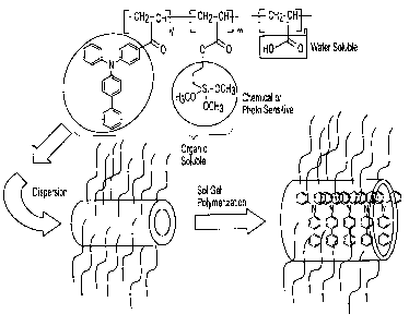
BRIEF DESCRIPTION OF THE DRAWINGS
[0029] The FIGURE is a schematic depiction of multi-block polymeric charge
transport materials at least partially embedded within carbon nanotube
materials.
EMBODIMENTS
[0030] Electrophotographic imaging members are known in the art.
Electrophotographic imaging members may be prepared by any suitable technique.
Typically, a flexible or rigid substrate is provided with an electrically
conductive surface.
A charge generating layer is then applied to the electrically conductive
surface. A charge
blocking layer may optionally be applied to the electrically conductive
surface prior to the
application of a charge generating layer. If desired, an adhesive layer may be
utilized
between the charge blocking layer and the charge generating layer. Usually the
charge
generation layer is applied onto the blocking layer and a hole or charge
transport layer is
formed on the charge generation layer, followed by an optional overcoat layer.
This
structure may have the charge generation layer on top of or below the hole or
charge
transport layer. In embodiments, the charge generating layer and hole or
charge transport
layer can be combined into a single active layer that performs both charge
generating and
hole transport functions.
[0031] The substrate may be opaque or substantially transparent and may
comprise any suitable material having the required mechanical properties.
Accordingly,
the substrate may comprise a layer of an electrically non-conductive or
conductive
material such as an inorganic or an organic composition. As electrically non-
conducting
materials there may be employed various resins known for this purpose
including
polyesters, polycarbonates, polyamides, polyurethanes, and the like which are
flexible as
thin webs. An electrically conducting substrate may be any metal, for example,
aluminum, nickel, steel, copper, and the like or a polymeric material, as
described above,
filled with an electrically conducting substance, such as carbon, metallic
powder, and the
like or an organic electrically conducting material. The electrically
insulating or
conductive substrate may be in the form of an endless flexible belt, a web, a
rigid
cylinder, a sheet and the like. The thickness of the substrate layer depends
on numerous
factors, including strength desired and economical considerations. Thus, for a
drum, this
CA 02595821 2007-08-01
8
layer may be of substantial thickness of, for example, up to many centimeters
or of a
minimum thickness of less than a millimeter. Similarly, a flexible belt may be
of
substantial thickness, for example, about 250 micrometers, or of minimum
thickness less
than 50 micrometers, provided there are no adverse effects on the final
electrophotographic device.
[0032] In embodiments where the substrate layer is not conductive, the surface
thereof may be rendered electrically conductive by an electrically conductive
coating.
The conductive coating may vary in thickness over substantially wide ranges
depending
upon the optical transparency, degree of flexibility desired, and economic
factors.
Accordingly, for a flexible photoresponsive imaging device, the thickness of
the
conductive coating may be about 20 angstroms to about 750 angstroms, such as
about 100
angstroms to about 200 angstroms for an optimum combination of electrical
conductivity,
flexibility and light transmission. The flexible conductive coating may be an
electrically
conductive metal layer formed, for example, on the substrate by any suitable
coating
technique, such as a vacuum depositing technique or electrodeposition. Typical
metals
include aluminum, zirconium, niobium, tantalum, vanadium and hafnium,
titanium,
nickel, stainless steel, chromium, tungsten, molybdenum, and the like.
[0033] An optional hole blocking layer may be applied to the substrate. Any
suitable and conventional blocking layer capable of forming an electronic
barrier to holes
between the adjacent photoconductive layer and the underlying conductive
surface of a
substrate may be utilized.
[0034] An optional adhesive layer may be applied to the hole blocking layer.
Any suitable adhesive layer known in the art may be utilized. Typical adhesive
layer
materials include, for example, polyesters, polyurethanes, and the like.
Satisfactory
results may be achieved with adhesive layer thickness of about 0.05 micrometer
(500
angstroms) to about 0.3 micrometer (3,000 angstroms). Conventional techniques
for
applying an adhesive layer coating mixture to the charge blocking layer
include spraying,
dip coating, roll coating, wire wound rod coating, gravure coating, Bird
applicator
coating, and the like. Drying of the deposited coating may be effected by any
suitable
CA 02595821 2010-12-20
9
conventional technique such as oven drying, infra red radiation drying, air
drying and
the like.
[0035] At least one electrophotographic imaging layer is formed on the
adhesive
layer, blocking layer or substrate. The electrophotographic imaging layer may
be a single
layer that performs both charge generating and hole or charge transport
functions as is
known in the art or it may comprise multiple layers such as a charge generator
layer and
charge transport layer. Charge generator layers may comprise amorphous films
of
selenium and alloys of selenium and arsenic, tellurium, germanium and the
like,
hydrogenated amorphous silicon and compounds of silicon and germanium, carbon,
oxygen, nitrogen and the like fabricated by vacuum evaporation or deposition.
The
charge generator layers may also comprise inorganic pigments of crystalline
selenium and
its alloys; Group I1-VI compounds; and organic pigments such as quinacridones,
polycyclic pigments such as dibromo anthanthrone pigments, perylene and
perinone
diamines, polynuclear aromatic quinones, azo pigments including bis-, tris-
and tetrakis-
azos; and the like dispersed in a film forming polymeric binder and fabricated
by solvent
coating techniques.
[0036] Phthalocyanines have been employed as photogenerating materials for
use in laser printers utilizing infrared exposure systems. Infrared
sensitivity is required
for photoreceptors exposed to low cost semiconductor laser diode light
exposure devices.
The absorption spectrum and photosensitivity of the phthalocyanines depend on
the
central metal atom of the compound. Many metal phthalocyanines have been
reported and
include, oxyvanadium phthalocyanine, chloroaluminum phthalocyanine, copper
phthalocyanine, oxytitanium phthalocyanine, chlorogallium phthalocyanine,
hydroxygallium phthalocyanine magnesium phthalocyanine and metal-free
phthalocyanine. The phthalocyanines exist in many crystal forms which have a
strong
influence on photogeneration.
[0037] Any suitable polymeric film forming binder material may be employed
as the matrix in the charge generating (photogenerating) binder layer. Typical
polymeric
film forming materials include those described, for example, in U.S. Patent
No.
3,121,006. Thus,
CA 02595821 2007-08-01
typical organic polymeric film forming binders include thermoplastic and
thermosetting
resins such as polycarbonates, polyesters, polyamides, polyurethanes,
polystyrenes,
polyarylethers, polyarylsulfones, polybutadienes, polysulfones,
polyethersulfones,
polyethylenes, polypropylenes, polyimides, polymethylpentenes, polyphenylene
sulfides,
polyvinyl acetate, polysiloxanes, polyacrylates, polyvinyl acetals,
polyamides,
polyimides, amino resins, phenylene oxide resins, terephthalic acid resins,
phenoxy
resins, epoxy resins, phenolic resins, polystyrene and acrylonitrile
copolymers,
polyvinylchloride, vinylchloride and vinyl acetate copolymers, acrylate
copolymers, alkyd
resins, cellulosic film formers, poly(amideimide), styrenebutadiene
copolymers,
vinylidenechloride-vinylchloride copolymers, vinylacetate-vinylidenechloride
copolymers, styrene-alkyd resins, polyvinylcarbazole, and the like. These
polymers may
be block, random or alternating copolymers.
[00381 The photogenerating composition or pigment is present in the resinous
binder composition in various amounts. Generally, however, from about 5
percent by
volume to about 90 percent by volume of the photogenerating pigment is
dispersed in
about 10 percent by volume to about 95 percent by volume of the resinous
binder, such as
from about 20 percent by volume to about 30 percent by volume of the
photogenerating
pigment dispersed in about 70 percent by volume to about 80 percent by volume
of the
resinous binder composition. In one embodiment about 8 percent by volume of
the
photogenerating pigment is dispersed in about 92 percent by volume of the
resinous
binder composition. The photogenerator layers can also be fabricated by vacuum
sublimation in which case there is no binder.
[00391 Any suitable and conventional technique may be utilized to mix and
thereafter apply the photogenerating layer coating mixture. Typical
application
techniques include spraying, dip coating, roll coating, wire wound rod
coating, vacuum
sublimation and the like. For some applications, the generator layer may be
fabricated in
a dot or line pattern. Removing of the solvent of a solvent coated layer may
be effected
by any suitable conventional technique such as oven drying, infrared radiation
drying, air
drying and the like.
CA 02595821 2010-12-20
11
100401 The charge transport layer comprises multi-block polymeric charge
transport materials at least partially embedded within carbon nanotube
materials. For
example, the multi-block polymeric charge transport material can include at
least a charge
transport block and a non-charge transport block, where one of the charge
transport block
and the non-charge transport block is embedded within the carbon nanotube
materials but
the other block is not embedded within the carbon nanotube materials. The non-
charge
transport block can be, for example, a block that assists in (such as
increases) water
solubility, a block that assists in (such as increases) organic solvent
solubility, or a block
that is responsive to chemical, photo, or physical stimuli to "lock" the
material in place in
relation to the carbon nanotube material. Of course, multiple non-charge
transport blocks
can also be included, such as to provide multiple of the above properties.
Alternatively, a
single non-charge transport block can be used that provides multiple of the
above
properties.
100411 In embodiments, the carbon nanotube material comprises carbon
nanotubes, carbon nanofibers, or variants thereof. As the carbon nanotube
material, any of
the currently known or after-developed carbon nanotube materials and variants
can be
used. Thus, for example, the carbon nanotubes can be on the order of from
about 0.1 to
about 50 nanometers in diameter, such as about 1 to about 10 nanometers in
diameter,
and up to hundreds of micrometers or more in length, such as from about 0.01
or about 10
or about 50 to about 100 or about 200 or about 500 micrometers in length. The
carbon
nanotube materials can be in multi-walled or single-walled forms, or a mixture
thereof.
In some embodiments, the carbon nanotube materials are particularly of the
single-walled
form. The carbon nanotubes can be either conducting or semi-conducting, with
conducting nanotubes being particularly useful in embodiments. Variants of
carbon
nanotubes include, for example, nanofibers, and are encompassed by the term
"carbon
nanotube materials" unless otherwise stated.
[00421 In addition, the carbon nanotubes of the present disclosure can include
only carbon atoms, or they can include other atoms such as boron and/or
nitrogen, such as
equal amounts of boron and nitrogen. Examples of carbon nanotube material
variants thus
include boron nitride, bismuth and metal chalcogenides. Combinations of these
materials
CA 02595821 2007-08-01
12
can also be used, and are encompassed by the term "carbon nanotube materials"
herein.
In embodiments, the carbon nanotube material is desirably free, or essentially
free, of any
catalyst material used to prepare the carbon nanotubes. For example, iron
catalysts or
other heavy metal catalysts are typically used for carbon nanotube production.
However,
it is desired in embodiments that the carbon nanotube material not include any
residual
iron or heavy metal catalyst material.
[0043] To provide desired charge transport, solubility, and other properties,
the
carbon nanotube materials are permanently ordered with multi-block polymers
that
include at least one charge transport block and at least one non-charge
transport block. In
embodiments, the separate block units of the multi-block polymers can be
randomly
scattered along the polymer chain, although an ordered multi-block polymer is
desired so
that the at least one charge transport block and at least one non-charge
transport block can
be desirably located with respect to the carbon nanotube materials. The multi-
block
polymers can include, for example from 2 to about 10 or more different types
of
monomer units, such as 2, 3, 4, or 5 different types of monomer units.
[0044] In embodiments, the different types of monomer units can be variously
located in the multi-block polymer chain with respect to the carbon nanotube
material.
For example, the different types of monomer units can be variously located
either inside
or outside of the carbon nanotube material. However, in one embodiment, the
multi-
block polymer is provided such that the charge transport block is located
inside the
carbon nanotube material, to provide increased charge transport properties,
while the non-
charge transport block or blocks are located outside of the carbon nanotube
material, to
provide, for example, increased solubility properties.
[0045] The multi-block polymers are permanently ordered with the carbon
nanotube materials. That is, for example, rather than simply being physically
associated
with the carbon nanotube materials, the multi-block polymers are chemically or
otherwise
attached or anchored to the carbon nanotube materials. In this manner, for
example, the
charge transport blocks are localized in the carbon nanotube materials to
provide the
increased charge transport properties, without a likelihood that the charge
transport
moieties will move within the structure and thus alter the charge transport
properties.
CA 02595821 2010-12-20
13
Alternatively, in embodiments, the charge transport blocks can be localized,
such as
attached, on the outer surface of the carbon nanotube materials to provide the
same
increased charge transport properties.
100461 The permanent ordering of the multi-block polymers with the carbon
nanotube materials can be achieved in any suitable manner, so long as the
multi-block
polymers are locked or "frozen" into place with respect to the carbon nanotube
materials.
This permanent ordering can be achieved, for example, by any of the various
chemical,
photo, or physical means that anchor the multi-block polymers to the carbon
nanotube
materials.
[00471 At least one block of the multi-block polymer is a charge transport
block. Suitable charge transport polymers containing charge transport blocks
include, for
example, polyvinylcarbazoles, polythiophenes, polysilanes, polyanilines,
poly(phenylene
vinylenes), polyphenylenes, poly(phenylene sulfides), polyanilines,
poly(phenylene
sulfide phenylenamine), copolymers thereof containing triarylamine charge
transport
groups, and mixtures thereof. In an embodiment, the arylamine charge transport
compound is a para-subsbtuted arylamine charge transport material. Such
arylamine
charge transport material may commonly have from I to about 10 nitrogen
centers per
repeating unit, however in embodiments the arylamine charge transport material
may
have about 1 to about 6, such as about I and about 2 nitrogen centers per
repeating unit.
Where there is more than 1 nitrogen atom, the nitrogen atoms generally are
covalently
linked by carbon residues, which are considered aromatic such that there is an
electronic
connection at an atomic or molecular level between the nitrogen atoms. Of
course, such
attachment is desired in embodiments, but is not necessary. Other suitable
charge
transport blocks for the multi-block polymers are described in, for example,
U.S. Patents
Nos. 4,806,443, 4,806,444, 4,818,650, 4,935,487, 4,956,440, 4,801,517,
4,806,444,
4,818,650, 4,806,443, and 5,030,532.
100481 At least one other block of the multi-block polymer is a non-charge
transport block. The non-charge transport block can be, for example, a block
that assists
in (such as increases) water solubility, a block that assists in (such as
increases) organic
CA 02595821 2010-12-20
14
solvent solubility, a block that is responsive to chemical, photo, or physical
stimuli to
"lock" the material in place in relation to the carbon nanotube material, or
the like. The
non-charge transport block can also provide multiple of these properties, if
desired.
[00491 For example, the multi-block polymer can include a non-charge
transport block that is responsive to chemical or photo stimulus, and which is
also at the
same time soluble in organic materials. Examples of chemical and photo
stimulus
include, for example, ability to cure by radiation exposure such as UV-
radiation
exposure; ability to react such as through a sol-gel process, a hydrosilation
reaction such
as hydrosilation of a vinyl groups with a hydridosilane, a peroxide activated
cure reaction
such as of a vinyl group, by a sol-gel reaction; or the like.
[00501 Accordingly, exemplary non-charge transport blocks in this category
include groups that are subject to sol-gel reaction, such as groups that
include alkylsiloxy
groups, silanol groups, chlorosilane groups, and the like. Such groups can
undergo a sol-
gel reaction with, for example, an alkoxysilane, a chlorosilane, a silanol-
terminated
polysiloxane, or the like. In the case of alkylsiloxy and alkoxysilane groups,
the alkyl
group can be, for example, from I to about 30 carbons in length, such as from
1 to about
20 or from 1 to about 10, such as 1, 2, 3, 4, or 5, and can be cyclic,
straight, or branched.
The group can also be substituted or unsubstituted, where the substitutions
can include
one or more groups selected from the group consisting of methyl, ethyl,
isobutyl, isooctyl,
cyclopentyl, cyclohexyl, vinyl, styrl, trimethylsiloxyl, trichlorosilylethyl,
trichlorosilylpropyl, dichiorosilylethyl, chlorosilylethyl, phenyl,
chlorobenzyl, cyanoethyl,
cyanopropyl, norbomenyl, fluoro, silanol, dimethylsilane, alkoxy,
methacrylate, silane,
aniline, amine, phenol, and alcohol.
100511 Other exemplary non-charge transport blocks in this category include
groups that are subject to curing, such as by ultraviolet radiation. Exemplary
radiation-
curable groups thus include acrylates; methacrylates; alkenes; allylic ethers;
vinyl ethers;
epoxides, such as cycloaliphatic epoxides, aliphatic epoxides, and glycidyl
epoxides;
oxetanes; stilbenes, derivatives of cinnamic acid such as esters or amides of
cinnamic
acid and the like, which can be provided in the form of acrylated esters,
acrylated
polyesters, acrylated ethers, acrylated polyethers, acrylated epoxies,
urethane acrylates,
CA 02595821 2007-08-01
pentaerythritol tetraacrylate, acrylated cinnamic acid and the like. Specific
examples of
suitable acrylated monomers include, but are not limited to, polyacrylates,
such as
trimethylol propane triacrylate, pentaerythritol tetraacrylate,
pentaerythritol triacrylate,
dipentaerythritol pentaacrylate, glycerol propoxy triacrylate, tris(2-
hydroxyethyl)
isocyanurate triacrylate, pentaacrylate ester, and the like, epoxy acrylates,
urethane
acrylates, amine acrylates, acrylic acrylates, and the like.
[0052] Other exemplary non-charge transport blocks that can be used include
blocks that assist in (such as increases) water solubility. Examples of such
blocks include
carboxylic acid groups, such as those having from 1 to about 20 carbon atoms,
such as
from 1 to about 15 or from 1 to about 10 carbon atoms. The block can have one
or more
carboxylic acid functionalities, such as 1, 2, 3, 4, or more carboxylic acid
functionalities.
Other examples of blocks that assist in water solubility or an increase in
hydrophillicity
are hydroxyl or sulfonic acid residues where said residues contain aliphatic
or aromatic
residues containing 1 to about 20 carbon atoms, such as from 1 to about 15 or
from 1 to
about 10 carbon atoms. The block can have one or more hydrophilic
functionality, such
as 1, 2, 3, 4, or more hydrophilic functionalities.
[0053] In one embodiment, the multi-block polymer includes charge transport
blocks, sol-gel functional non-charge transport blocks, and water soluble non-
charge
transport blocks. Such a multi-block polymer can generally be represented by
the
formula:
(CTB)a(NCTB 1)b(NCTB2)c
where CTB represents the charge transport block, NCTB I represents the sol-gel
functional non-charge transport blocks, NCTB2 represents the water soluble non-
charge
transport blocks, and a, b, and c represent average number of monomer units.
In
embodiments, the subscripts a, b, and c in the above formula can be, for
example, each in
a range of from about 1 to about 98, such as in a ratio of a:b:c varying from
about 1:1:98
to 1:98:1 to 98:1:1 depending on the nature of the multi-block polymer and the
desired
application. Additionally the total multi-block polymer may have a molecular
weight as
low as about 1,000 Daltons to as high as about 1,000,000 Daltons, again
depending on the
nature of the multi-block polymer and its intended application.
CA 02595821 2007-08-01
16
[00541 The FIGURE represents, schematically, only one exemplary
embodiment. In the schematic, multi-block polymers generally of the formula
above is
permanently ordered with a carbon nanotube. As shown in the figure, the charge
transport block of the multi-block polymer is located inside the carbon
nanotube, while
the sot-gel functional non-charge transport block and the water soluble non-
charge
transport block are both located outside of the carbon nanotube. The
morphology of the
components is then locked-in, or frozen, by a sol-gel reaction with the sol-
gel functional
non-charge transport blocks.
[00551 The multi-block polymer and carbon nanotube material structure can be
used in place of, or in addition to, conventional charge transport materials
in the charge
transport layer. When the multi-block polymer and carbon nanotube material
structure is
used in addition to convention charge transport materials, the convention
charge transport
materials can be, for example, charge transporting small molecules dissolved
or
molecularly dispersed in a film forming electrically inert polymer such as a
polycarbonate. The term "dissolved" as employed herein is defined herein as
forming a
solution in which the small molecule is dissolved in the polymer to form a
homogeneous
phase. The expression "molecularly dispersed" as used herein is defined as a
charge
transporting small molecule dispersed in the polymer, the small molecules
being
dispersed in the polymer on a molecular scale. Any suitable charge
transporting or
electrically active small molecule may be employed in the charge transport
layer. The
expression charge transporting "small molecule" is defined herein as a monomer
that
allows the free charge photogenerated in the transport layer to be transported
across the
transport layer. Typical charge transporting small molecules include, for
example,
pyrazolines such as 1-phenyl-3-(4'-diethylamino styryl)-5-(4"-diethylamino
phenyl)pyrazoline, diamines such as N,N'-diphenyl-N,N'-bis(3-methylphenyl)-
(1,1'-
biphenyl)-4,4'-diamine, hydrazones such as N-phenyl-N-methyl-3-(9-
ethyl)carbazyl
hydrazone and 4-diethyl amino benzaldehyde-1,2-diphenyl hydrazone, and
oxadiazoles
such as 2,5-bis (4-N,N'-diethylaminophenyl)-1,2,4-oxadiazole, stilbenes and
the like. As
indicated above, suitable electrically active small molecule charge
transporting
compounds are dissolved or molecularly dispersed in electrically inactive
polymeric film
CA 02595821 2010-12-20
17
forming materials. Small molecule charge transporting compounds that permit
injection
of holes from the pigment into the charge generating layer with high
efficiency and
transport them across the charge transport layer with very short transit times
are N,N'-
diphenyl-N,N'-bis(3 -methylphenyl)-(1,1'-biphenyl)-4,4'-diamine, N,N,N',N'-
tetra-p-
tolylbiphenyl-4,4'-diamine, and N,N'-Bis(3-methylphenyl)-N,N'-bis[4-(1-
butyl)phenyl]-
[p-terphenyl] -4,4' -diamine.
[0056] The charge transport layer of the photoreceptor can include the multi-
block polymer and carbon nanotube material structure in any desired and
suitable amount.
[0057] A benefit of the use of multi-block polymeric charge transport
materials
at least partially embedded within carbon nanotube materials in charge
transport layers is
that the materials exhibit very high charge transport mobility. Accordingly,
the use of
multi-block polymeric charge transport materials at least partially embedded
within
carbon nanotube materials in a charge transport layer can provide charge
transport speeds
that are orders of magnitude higher than charge transport speeds provided by
conventional charge transport materials. For example, the charge transport
mobility in a
charge transport layer comprising multi-block polymeric charge transport
materials at
least partially embedded within carbon nanotube materials can be 1, 2, 3, 4,
5, 6, 7, or
more, such as about 1 to about 4, orders of magnitude higher as compared to a
comparable charge transport layer that includes a similar amount of
conventional
pyrazoline, diamine, hydrazones, oxadiazole, or stilbene charge transport
small
molecules. This resultant dramatic increase in charge mobility can result in
significant
corresponding improvements in the printing process and apparatus, such as
extreme
printing speeds, increased print quality, and increased photoreceptor
reliability.
[0058] Additional details regarding carbon nanotubes and their charge
transport
mobilities can be found, for example, in T. Durkop et al., "Extraordinary
Mobility in
Semiconducting Carbon Nanotubes," Nano. Lett., Vol. 4, No. 1, 35-39 (2004).
[0059] Any suitable electrically inactive resin binder insoluble in the
alcohol
solvent used to apply an optional overcoat layer may be employed in the charge
transport
layer. Typical inactive resin binders include polycarbonate resin, polyester,
polyarylate,
CA 02595821 2007-08-01
18
polysulfone, and the like. Molecular weights can vary, for example, from about
20,000 to
about 150,000. Exemplary binders include polycarbonates such as poly(4,4'-
isopropylidene-diphenylene)carbonate (also referred to as bisphenol-A-
polycarbonate,
poly(4,4'-cyclohexylidinediphenylene) carbonate (referred to as bisphenol-Z
polycarbonate), poly(4,4'-isopropylidene-3,3'-dimethyl-diphenyl)carbonate
(also referred
to as bisphenol-C-polycarbonate) and the like. Any suitable charge
transporting polymer
may also be utilized in the charge transporting layer. The charge transporting
polymer
should be insoluble in any solvent employed to apply the subsequent overcoat
layer
described below, such as an alcohol solvent. These electrically active charge
transporting
polymeric materials should be capable of supporting the injection of
photogenerated holes
from the charge generation material and be incapable of allowing the transport
of these
holes therethrough.
[0060] Any suitable and conventional technique may be utilized to mix and
thereafter apply the charge transport layer coating mixture to the charge
generating layer.
Typical application techniques include spraying, dip coating, roll coating,
wire wound rod
coating, and the like. Drying of the deposited coating may be effected by any
suitable
conventional technique such as oven drying, infra red radiation drying, air
drying and the
like.
[0061] Generally, the thickness of the charge transport layer is between about
and about 50 micrometers, but thicknesses outside this range can also be used.
The
charge transport layer should be an insulator to the extent that the
electrostatic charge
placed on the charge transport layer is not conducted in the absence of
illumination at a
rate sufficient to prevent formation and retention of an electrostatic latent
image thereon.
In general, the ratio of the thickness of the charge transport layer to the
charge generator
layers is desirably maintained from about 2:1 to 200:1 and in some instances
as great as
400:1. The charge transport layer, is substantially non-absorbing to visible
light or
radiation in the region of intended use but is electrically "active" in that
it allows the
injection of photogenerated holes from the photoconductive layer, i.e., charge
generation
layer, and allows these holes to be transported through itself to selectively
discharge a
surface charge on the surface of the active layer.
CA 02595821 2010-12-20
19
[00621 To improve photoreceptor wear resistance, a protective overcoat layer
can be provided over the photogenerating layer (or other underlying layer).
Various
overcoating layers are known in the art, and can be used as long as the
functional
properties of the photoreceptor are not adversely affected.
[0063] Also, included within the scope of the present disclosure are methods
of
imaging and printing with the imaging members illustrated herein. These
methods
generally involve the formation of an electrostatic latent image on the
imaging member;
followed by developing the image with a toner composition comprised, for
example, of
thermoplastic resin, colorant, such as pigment, charge additive, and surface
additives,
reference U.S. Patents Nos.4,560,635, 4,298,697 and 4,338,390, subsequently
transferring
the image to a suitable substrate; and permanently affixing the image thereto.
In those
environments wherein the device is to be used in a printing mode, the imaging
method
involves the same steps with the exception that the exposure step can be
accomplished
with a laser device or image bar.
[0064] It will be appreciated that various of the above-disclosed and other
features and functions, or alternatives thereof, may be desirably combined
into many
other different systems or applications. Also that various presently
unforeseen or
unanticipated alternatives, modifications, variations or improvements therein
may be
subsequently made by those skilled in the art which are also intended to be
encompassed
by the following claims.