Note: Descriptions are shown in the official language in which they were submitted.
CA 02595944 2007-07-25
WO 2007/008349 PCT/US2006/023924
TWO STAGE MICROWAVE
CLASS E POWER AMPLIFIER
BACKGROUND OF THE INVENTION
Field of the Invention:
The present invention relates to electrical and electronic circuits and
systems.
More specifically, the present invention relates to microwave Class E power
amplifiers.
Description of the Related Art:
Highly efficient microwave and radio frequency (RF) high power amplifiers
are required for many commercial and military applications. Typical
applications
include wireless local area networks, cellular phones and telecommunication
systems,
as well as advanced airborne active phased array radar systems. Class-E power
amplifiers are high-efficiency amplifiers that would be useful for these and
other
applications.
Class-E amplifiers are part of the "switching mode amplifiers" such as class
D, E, F, etc. These types of amplifiers include a transistor that operates as
a perfect
switch with no overlapping voltage and current waveforms at its output
terminal,
thereby ideally dissipating zero DC power. Other classes of amplifiers such as
class
A, A/B and C, operate as current-sources with overlapping voltage and current
waveforms and hence dissipate DC power, leading to a lower efficiency.
A Class-E amplifier typically consists of a single transistor and a resonant
load
CA 02595944 2007-07-25
WO 2007/008349 PCT/US2006/023924
network. The function of the load network is to shape the voltage and current
waveforms at the active device output terminal to prevent simultaneous high
voltage
and high current in the transistor, thereby minimizing DC power dissipation.
The
active device acts as a switch, driven by an RF input signal to "ON" and "OFF"
conditions. The operating point of the device is such that the device is
either OFF (in
the pinched-off region) or ON (in the linear region). Under an ideal switching
operation condition, output voltage and current waveforms at the device output
terminal do not exist simultaneously and, therefore, the energy dissipated
within the
device is zero, yielding a 100 percent theoretical power conversion
efficiency.
Present class-E high power amplifiers (HPAs) have limited useful bandwidth
due to their highly tuned load circuits. Class-E HPAs have generally been used
at
audio, HF and UHF frequencies for applications such as audio HI-FI systems,
Ham
radios and high power plasma generation where narrow frequency bandwidth are
required. In recent years, the published work on monolithic class-E power
amplifiers
has been limited to narrow band (less than 500 MHz) RF frequencies covering
the
hand set cell phone market.
In addition, conventional class-E amplifiers have limited power outputs.
Class-E amplifiers are typically implemented using single stage designs. In
order to
increase gain, the size of the amplifier's active device is increased.
Increasing the
active device, however, reduces the frequency range of the amplifier due to
the
increased capacitance at the input of the device.
Hence, a need exists in the art for an improved Class-E amplifier offering
simultaneous high power and high power added efficiency (PAE) over a broader
frequency range.
2
CA 02595944 2010-11-03
SUMMARY OF THE INVENTION
The need in the art is addressed by the load circuit of the present invention.
The
novel load circuit is adapted for use with any switching mode circuit and
includes a series
inductive-capacitive network coupled to an output of the switching mode
circuit and a circuit
for providing a capacitance coupled to the output of the switching mode
circuit. In an
illustrative embodiment, the circuit for providing capacitance includes one or
more lumped
capacitors adapted to compensate for an intrinsic capacitance in the switching
mode circuit.
The load circuit may also include a shunt inductance coupled to the output of
the switching
mode circuit.
In an illustrative embodiment, the load circuit is adapted to provide a Class-
E load to
a two-stage Class-E high power amplifier. The amplifier includes a driver
stage, a novel
Class-E inter-stage matching network (ISMN), and a high power stage using the
novel load
circuit. The novel ISMN includes a first circuit for providing a Class-E load
to the amplifier
driver stage and a second circuit for providing a matched input impedance for
the high power
stage. The load circuit and the ISMN are both adapted to provide simultaneous
high power
added efficiency and high power over a broad frequency range.
Accordingly, in one aspect of the present invention there is provided a load
circuit for
use with a switching mode circuit comprising:
a series inductive-capacitive network coupled to an output of said switching
mode
circuit;
one or more lumped capacitors coupled to said output of said switching mode
circuit;
and
an impedance transformer coupled to said series inductive-capacitive network,
said
impedance transformer transforming an output impedance of said load circuit to
match an
impedance of a desired load.
According to another aspect of the present invention there is provided an
inter-stage
matching network for coupling a first circuit with a second circuit
comprising:
first means for providing a Class-E load to said first circuit; and
second means for providing a matched input impedance for said second circuit,
wherein said inter-stage matching network is operable at frequencies in the
range of 7-11
GHz.
3
CA 02595944 2010-11-03
According to yet another aspect of the present invention there is provided a
two-stage
Class-E high power amplifier comprising:
a driver stage, including an active device;
a high power stage; and
an inter-stage matching network disposed between said driver stage and said
high
power stage and adapted to provide a Class-E load to said driver stage and a
matched input
impedance for said high power stage, wherein said inter-stage matching network
includes a
series inductive-capacitive network for providing the Class-E load coupled to
an output of
said active device.
BRIEF DESCRIPTION OF THE DRAWINGS
Fig. 1 is a simplified block diagram of an illustrative embodiment of a two-
stage
Class-E high power amplifier designed in accordance with the teachings of the
present
invention.
Fig. 2a is a simplified schematic diagram of a discrete component
implementation of
an amplifier with a conventional Class-E load.
Fig. 2b is a distributed component implementation of the conventional Class-E
3a
CA 02595944 2007-07-25
WO 2007/008349 PCT/US2006/023924
load depicted in Fig. 2a.
Fig. 3 is a simplified schematic diagram of a discrete component
implementation of a prior art broadband Class-E load network.
Fig. 4 is a simplified schematic diagram of a discrete component
implementation of an illustrative embodiment of a Class-E load network
designed in
accordance with the teachings of the present invention.
Fig. 5 is a distributed component implementation of the Class-E load depicted
in Fig. 4.
Fig. 6 is a graph showing the frequency response of the distributed load of
Fig.
5.
Fig. 7 is a representation of a Class-E ISMN in accordance with the teachings
of
the present invention.
Fig. 8a is a simplified schematic diagram showing a distributed component
implementation of an illustrative embodiment of the first amplifier stage and
a first
circuit of the Class-E ISMN designed in accordance with the teachings of the
present
invention.
Fig. 8b is a simplified schematic diagram showing a distributed component
implementation of an illustrative embodiment of a second circuit of the Class-
E
ISMN and the second amplifier stage designed in accordance with the teachings
of the
present invention.
DESCRIPTION OF THE INVENTION
Illustrative embodiments and exemplary applications will now be described with
reference to the accompanying drawings to disclose the advantageous teachings
of the
present invention.
While the present invention is described herein with reference to illustrative
embodiments for particular applications, it should be understood that the
invention is not
4
CA 02595944 2007-07-25
WO 2007/008349 PCT/US2006/023924
limited thereto. Those having ordinary skill in the art and access to the
teachings
provided herein will recognize additional modifications, applications, and
embodiments
within the scope thereof and additional fields in which the present invention
would be of
significant utility.
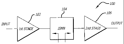
Fig. 1 is a simplified block diagram of an illustrative embodiment of a two-
stage
Class-E high power amplifier 100 designed in accordance with the teachings of
the
present invention. The circuit 100 is specifically synthesized for high power
operation
(5.0 W -10.0 W or greater), providing a simultaneous high power added
efficiency
(PAE) and high power over a broad frequency range (7-11 GHz). The amplifier
100
includes a driver stage (first stage) 102, a high power stage (second stage)
106, and a
novel class-E inter-stage matching network (ISMN) 104 situated between the two
stages.
Both stages of the amplifier 100 possess unique broadband class-E loads. This
design
approach is contrary to the conventional class AB HPA designs in which the
driver stage
is designed to operate in the linear region.
The two-stage Class-E high power amplifier (HPA) of the present invention
includes a novel Class-E load designed to maintain simultaneous high power and
high
PAE over a broad bandwidth. Fig. 2a is a simplified schematic diagram of a
discrete
component implementation of an amplifier 10 with a conventional Class-E load
20.
As shown in Fig. 2a, a typical Class-E amplifier 10 includes a transistor
represented
by a switch 12, coupled to a voltage source Vds via an inductive bias line 14.
The
switch 12 is also coupled to a resistive load 24 via a capacitor 22 and an
inverted L
type (series L, shunt C) wave shaping load network 20. The conventional Class-
E
load network 20 includes a first shunt capacitor 15, which is the drain to
source
capacitance (Cds) of the transistor switch 12, and a series inductor 16
followed by a
shunt capacitor 18. Few design efforts have been made to optimize these
circuits for
broadband operation. Hence, in previous amplifier designs, the drain bias line
14 was
treated independent of the load circuit 20, merely acting as a choke realized
by a
quarter wavelength length of transmission line.
Fig. 2b is a distributed component implementation of the conventional Class-E
load depicted in Fig. 2a. It is worth mentioning that the function of the load
network
5
CA 02595944 2009-08-17
in the class E amplifier is to shape the voltage and current waveforms.
Therefore, for
the design of a broadband Class-E amplifier, care should be taken to ensure
Class-E
waveforms exist over the entire frequency band. Conventional Class-E load
circuits
are operable only over a narrow bandwidth (about 500 MHz or less).
Fig. 3 is a simplified schematic diagram of a discrete component
implementation of a prior art broadband Class-E load network 30, as described
in
U.S. Patent No. 7,345,539 to Tayrani et al. issued on March 18, 2008. This
load
topology is based on a series L-C (inductive-capacitive) network, and includes
an
inductive element 32 connected in series with a capacitive element 34 between
the
transistor output terminal 36 and the resistive load 24. The drain bias line
is also
included in the load design process as a shunt inductive element 14 coupled to
the
transistor output terminal 36. The intrinsic capacitance Cds of the active
device is
represented as a shunt capacitor 15 couple to the transistor output terminal
36.
While this design provides superior broadband performance for medium
power applications, it may not be as effective for high power amplifiers. In
order to
achieve greater RF power, a high power amplifier typically includes a larger
active
device (gate periphery greater than 5.0 mm), which generally is realized by
combining several active devices in parallel. However, care must typically be
taken
in combining active devices in parallel as it may reduce the useful frequency
range of
the amplifier due to the intrinsic capacitance and other associated device
extrinsic
parasitics, thereby further reducing the operational bandwidth of the circuit.
In accordance with the teachings of the present invention, auxiliary
capacitors are
added to a series L-C load network to compensate for the intrinsic capacitance
of the
active device. Fig. 4 is a simplified schematic diagram of a discrete
component
implementation of an illustrative embodiment of a Class-E load network 40
designed
in accordance with the teachings of the present invention. The novel load
network 40
includes one or more lumped capacitors 42 coupled to the output terminal 36 of
the
active device. The lumped capacitors 42 are designed to compensate for the
intrinsic
6
CA 02595944 2007-07-25
WO 2007/008349 PCT/US2006/023924
active device capacitance Cd (represented in Fig. 4 as a shunt capacitor 15
coupled to
the transistor output terminal 36). An inductive element 32 is connected in
series
with a capacitive element 34 between the transistor output terminal 36 and a
broadband impedance transformer 44. The impedance transformer 44 transforms
the
output impedance of the circuit to match the impedance of the resistive load
24, which
in the illustrative embodiment is 50.0 Ohms. The drain bias line is also
included in
the load design process as a shunt inductive element 14 coupled to the
transistor
output terminal 36.
The lumped load shown in Fig. 4 has to be transformed to its equivalent
distributed network to render it useful for application at X-band and other
microwave
frequency bands. To optimize the distributed load for Class-E operation, a
time domain
optimization process is performed. Further details on a design methodology for
broadband circuits can be found in the above referenced patent application.
Fig. 5 is a distributed component implementation of the Class-E load depicted
in Fig. 4. The load network 40 shown in Fig. 5 is designed for use in the
second stage
106 of the novel high power amplifier 100 of Fig. 1. In the illustrative
embodiment,
the second amplifier stage 106 includes four transistors 50A, 50B, 50C, and
50D
connected in parallel. The outputs (drains) of the transistors are connected
together at
node 36. In this embodiment, the load network 40 includes two adjustable
lumped
capacitors 42A and 42B coupled to node 36. Two bias drain lines 14A and 14B
couple the transistor output node 36 to voltage sources V1 and V2,
respectively. The
series L-C network is implemented by two transmission lines 52A and 52B, which
couple the transistor output node 36 to a three-port capacitor 54. A
transmission line
56 couples the three-port capacitor 54 to the impedance transformer 44. The
impedance transformer 44 is implemented using two transmission lines 58 and 60
connected in series between line 56 and an output terminal 62. A shunt
capacitor 64
is connected between lines 56 and 58, and a shunt capacitor 66 is connected
between
lines 58 and 60. Illustrative values for the width and length dimensions of
the
transmission lines are shown in microns in Fig. 5. Other implementations may
also
be used without departing from the scope of the present teachings.
7
CA 02595944 2007-07-25
WO 2007/008349 PCT/US2006/023924
The novel Class-E load 40 of the present invention is suitable for high power
operation, and is especially useful for large active devices, as used in the
second stage
of the illustrative HPA of Fig. 1. The circuit 40 provides a simultaneous high
PAE
and high power over a broadband frequency range (7-11 GHz in the illustrative
embodiment). Fig. 6 is a graph showing the frequency response of the
distributed
load 40 of Fig. 5, illustrating a broadband nearly frequency independent phase
and
magnitude response over the frequency range 7-11 GHz. This type of frequency
response is the necessary requirement to the broadband operation of a Class-E
HPA.
Those of ordinary skill in the art may extend the present teachings to other
frequencies without departing from the scope thereof.
Returning to Fig. 1, the two-stage Class-E high power amplifier 100 of the
present invention also includes a novel Class-E inter-stage matching network
(ISMN)
104 designed to maintain simultaneous high power and high PAE over a broad
bandwidth. An ISMN is necessary when designing a two-stage amplifier. The ISMN
circuit could be said is similar to a band-pass filter having unequal complex
loads at its
input/output ports. In the case of the Class-E ISMN circuit 104, the complex
load has to
be a frequency independent Class-E load. This load (which is the Class-E load
for the
first amplifier stage 102) then is matched to the complex input impedance of
the second
amplifier stage 106 over the desired bandwidth. Fig. 7 is a representation of
a Class-E
ISMN 104, illustrating this concept.
The novel Class-E ISMN 104 includes a first circuit 110 for providing a Class-
E
load to the first amplifier stage 102, and a second circuit 112 for providing
a matched
input impedance for the second amplifier stage 106. Figs. 8a and 8b show the
details for
the novel two-stage Class-E HPA 100 of the present invention: Fig. 8a shows
the first
amplifier stage 102 and the first portion 110 of the ISMN, and Fig. 8b shows
the second
portion 112 of the ISMN and the second amplifier stage 106.
Fig. 8a is a simplified schematic diagram showing a distributed component
implementation of an illustrative embodiment of the first amplifier stage 102
and first
circuit 110 of the Class-E ISMN designed in accordance with the teachings of
the
present invention. The first amplifier stage 102 includes an active device 124
and an
8
CA 02595944 2007-07-25
WO 2007/008349 PCT/US2006/023924
input matching network 122 for coupling an input terminal 120 to the input of
the active
device 124. In the illustrative embodiment, the active device 124 is a pseudo-
morphic,
high-electron mobility transistor (pHEMT). The output (drain) of the active
device
124 is connected to the first circuit 110 of the ISMN.
The first circuit 110 of the ISMN provides a broadband Class-E load to the
first
amplifier stage 102. In the illustrative embodiment, the circuit 110 is based
on a series L-
C network and includes a transmission line 128 connected in series with a
capacitive
element 130 between the active device output 126 and a node 132. Two
transmission
lines 134 and 136 are connected in series between the transistor output 126
and a voltage
supply V3. A shunt capacitor 144 is coupled between the lines 134 and 136.
Three
transmission lines 138, 140 and 142 are connected in series between the
transistor output
126 and ground.
Optionally, the first circuit 110 of the ISMN may also include auxiliary
lumped
capacitors coupled to the transistor output 126 to compensate for the
intrinsic capacitance
of the active device 124. The first circuit 110 of the ISMN thus uses a
similar approach
as the Class-E load described above. In the illustrative embodiment, auxiliary
capacitors
are not needed in the ISMN because the first amplifier stage 102 is a driver
stage
providing lower power (and therefore a smaller active device 124) than the
second
amplifier stage 106. The addition of auxiliary lumped capacitors to the first
circuit 100
of the ISMN may be desirable for a higher power first amplifier stage or for
higher
frequency operation.
Fig. 8b is a simplified schematic diagram showing a distributed component
implementation of an illustrative embodiment of the second circuit 112 of the
Class-E
ISMN and the second amplifier stage 106 designed in accordance with the
teachings of
the present invention. In the illustrative embodiment, the second amplifier
stage 106
includes four active devices 50A, 50B, 50C, and 50D connected in parallel, and
a
broadband Class-E load 40, the details of which were shown in Fig. 5. In the
illustrative
embodiment, the active devices 50A, 50B, 50C, and 50D are implemented using
pHEMTs.
The second circuit 112 of the ISMN provides matched input impedances to the
9
CA 02595944 2007-07-25
WO 2007/008349 PCT/US2006/023924
inputs of the active devices 50A, 50B, 50C, and 50D in the second amplifier
stage 106.
In the illustrative embodiment, the second circuit 112 includes four
transmission lines
150, 152, 154, and 156 connected in series between the node 132 and the input
of the
transistor 50A. A three-port junction 158 connects the lines 154 and 156 to a
transmission line 160, which is coupled to a voltage supply V5. A shunt
capacitor 162 is
coupled between lines 150 and 152, and a shunt capacitor 164 is coupled
between lines
152 and 154. A shunt capacitor 166 is coupled to node 132. Two transmission
lilies 170
and 172 are connected in series between the capacitor 162 and the input of
transistor
50B. A shunt capacitor 174 is coupled between lines 170 and 172.
Similarly for the other two transistors, four transmission lines 180, 182,
184, and
186 are connected in series between the node 132 and the input of the
transistor 50D. A
three-port,junction 188 connects the lines 184 and 186 to a transmission line
190, which
is coupled to a voltage supply V6. A shunt capacitor 192 is coupled between
lines 180
and 182, and a shunt capacitor 194 is coupled between lines 182 and 184. Two
transmission lines 200 and 202 are connected in series between the capacitor
192 and the
input of transistor 50C. A shunt capacitor 204 is coupled between lines 200
and 202.
Thus, the present teachings provide an efficient high power, broadband HPA by
synthesizing a new class of miniature broadband Class-E loads that are
technology
independent and therefore are suitable for monolithic integration in GaAs, GaN
and/or
SiGe MMIC technologies. The most important properties of these new loads are
their
ability to provide a simultaneous PAE and power over the entire bandwidth. In
a
preferred embodiment, the HPA is designed using a circuit simulation technique
including time domain analysis, Harmonic Balance analysis, large signal
stability
analysis, and envelop simulation. By applying these new circuits and their
associated
unique design methodology for the design of switching mode power amplifiers,
highly
efficient (PAE>80 at X-band) HPAs can be designed.
Thus, the present invention has been described herein with reference to a
particular embodiment for a particular application. Those having ordinary
skill in the
art and access to the present teachings will recognize additional
modifications,
applications and embodiments within the scope thereof. For example, the
present
CA 02595944 2007-07-25
WO 2007/008349 PCT/US2006/023924
teachings are not limited to Class-E amplifiers. That is, the present
teachings may be
used in connection with any switching amplifier or circuit design.
It is therefore intended by the appended claims to cover any and all such
applications, modifications and embodiments within the scope of the present
invention.
Accordingly,
11