Note: Descriptions are shown in the official language in which they were submitted.
CA 02596269 2007-08-21
PROCESS, VOLTAGE, TEMPERATt1RE INDF.PF.NDENT
SWITCHED DELAY COMPENSATION SCHEME
This application is a divisional application of co-pending
application 2,242,209, filed June 30, 1998.
FIELD OF THE INVENTION
This invention relates to circuits in which fine
delay elements are swapped with a coarse delay element
during tracking, such as in a delay locked loop (DLL),
and more particularly to a circuit and method for
compensating for tracking differences between switchable
coarse and fine delay elements.
BACKGROUND TO THE INVENTION
A digital delay locked loop is generally formed
of a phase detector which detects the phase difference
between a system clock and a feedback clock, and causes
adjustment of a time delay circuit in the loop which
causes the DLL output clock to~be adjusted to lock with
the system clock. The time delay is generally formed of
an adjustable delay line.
Since the delay line is typically adjusted in
steps, the finest delay resolution depends on the delay
line step increments. In order to hold the locked
condition, the delay line is continuously increased and
decreased in step increments around a lock point, which
results in inherent tracking jitter. In order to
decrease the jitter, the delay line has been formed of
plural coarse delay elements (CDE), forming a coarse
delay line, in series with plural fine delay elements
(FDE). After power-up of the circuit, the coarse delay
line is adjusted, and once a lock point has almost been
determined, the fine delay line is adjusted, which
narrows the window around the lock point, to about 25
picoseconds, which represents the nominal amount of
jitter in a typical applications.
One fine delay line element (FDE) consists of 32
steps x 25 picoseconds resulting in a time delay of about
1
CA 02596269 2007-08-21
0.8 ns, which approximately equals the time delay of a
single stage of the coarse delay line. Once the delay
locked loop has stabilized to the lock point, the delay
line will automatically compensate for variations in
delay caused by changing temperature and voltage
conditions, by varying the fine delay line.
The fine delay line is reset to the halfway point
after which it begins tracking.
In case of major drift, adjustments in the fine
delay line will overrun its end. In that case, another
coarse delay element is switched in series or an existing
coarse delay element is switched out of the coarse delay
line, and at the same time the fine delay line is
adjusted to compensate for the coarse delay increase or
decrease to provide the same total delay as before.
However, now the fine delay line can be used again to
compensate changes without immediate danger of overrun.
U.S. patent 5,544,203 invented by Casasanta et
al, and U.S. patent 5,604,775 each discuss adjustment of
a delay locked loop delay line using coarse and fine
adjustment. However, none address the problem solved by
the present invention, as will be elaborated below.
It is assumed in the prior art that interchanging
(switching) the fine delay line steps for a coarse delay
element provides an equal exchange of delay. Indeed, any
differences between the two appear as jitter of about 300
ps on the DLL output clock. This amount of jitter was
considered to be tolerable, given the prior art primary
application of single data rate synchronous dynamic
random access memories (SDRAMS). However, with the
advent of tighter access time (TaJ specifications for
double data rate (DDR) SDRAMs which are synchronized to
the rising and falling edges of a system clock rather
2
CA 02596269 2007-08-21
than only to the rising edge, even an amount of jitter of
200ps - 300ps is becoming intolerable, considering the
numerous sources adding to this jitter apart from the
DDL, including input clock to data skew, clock duty cycle
variations, inaccuracies in the actual input and output
buffer delays with respect to its design model, etc.
DLL jitter itself consists of factors such as
inherent tracking jitter and supply noise and substrate
noise induced jitter. The inherent tracking jitter is
caused by the up and down adjustments to the fine delay
line while the DLL is in the locked condition, and as
described above, is a variation equivalent to the delay
achieved throug a single step in the delay line. The
jitter caused by switching between the coarse and fine
delay elements caused by the mismatch between the
elements is referred to as a switching jitter. This
mismatch is highly dependent on the manufacturing
process, and thus is hard to predict in the design stage.
As the operating frequencies continue to increase, the
switching jitter can undesirably reduce the data eye
significantly. In addition, since this switching occurs
only infrequently, it is inherently hard to detect during
testing and can cause apparently randomly dropped bits
when the part is in use in the~field.
Analog techniques can be used to achieve a wide
range of fine resolution tracking for various
applications. In particular DLLs based on phase mixers
have been shown to achieve high fine resolution tracking
range through quadrature mixing. However, most analog
based DLL designs employ some form of charge pumps for
voltage controlled delay lines and as such they suffer
from a limited resolution of the delay steps since the
controlling element affects an entire delay line. In
3
CA 02596269 2007-08-21
=
addition such DLLs often require a large acquisition time
due to loop bandwidths being limited to a small fraction
of the clock frequency to ensure stability of the loop.
This effect also causes a poor jitter performance in
analog DLLs.
Furthermore, analog DLL designs are inherently
more susceptible to all sources of noise as their control
variables (usually voltage) are reduced to achieve finer
resolutions. In particular, SDRAMs provide a very noisy
environment for analog blocks in form of supply and
substrate noise, which when combined with area
restrictions in SDRAMs, sometimes preventing adequate
implementation of noise prevention techniques through
layout, can result in unreliable DLLs in noisy field
environments.
SUMMARY OF THE INVENTION
The present invention provides a circuit and a
method of allowing a DLL to track with fine resolution
delay elements, while providing a tracking range much
larger than that provided by the fine delay line without
the danger of producing switching jitter. The present
invention accomplishes this by determining substantially
the exact amount of fine delay line to compensate for a
coarse delay element. This determination is done by
providing a model of a coarse delay element and
indicating to the fine delay line control the amount of
fine delay to switch to substantially accurately
substitute for the coarse delay element.
In accordance with an embodiment of the
invention, a delay compensation circuit for a delay
locked loop which includes a main delay line having a
fine delay line comprising fine delay elements and a
coarse delay line comprising coarse delay elements, the
4
CA 02596269 2007-08-21
main delay line being controlled by a controller, the
delay compensation circuit comprises:
(a) an adjustable fine delay for modeling a coarse
delay element,
(b) a counter for controlling the adjustable fine
delay to a value which is substantially the same as that
of a coarse delay element,
(c) a circuit for applying a representation of the
system clock to the delay compensation circuit, and
(d) a circuit for applying the fine delay count from
the counter to the controller for adjusting the fine
delay line of the main delay line to a value which is
substantially the same as that of a coarse delay element
of the main delay line.
In accordance with another embodiment, a method
of compensating for fine delay jitter in a clock driven
main delay locked loop which includes coarse and fine
delay elements, comprises feeding the clock through a
first delay path having a number of fine delay elements
each having an adjustable number of fine delay steps,
feeding the clock through a second reference delay path
having a coarse delay element, detecting a phase
difference between outputs of the first and second delay
paths and controlling a counter thereby, adjusting the
number of fine delay steps to accurately compensate delay
through the coarse delay element, and controlling fine
delay in the main delay locked loop from the counter so
as to minimize fine delay jitter in the main delay locked
loop.
In accordance with another embodiment, a method
of compensating for fine delay jitter in a main circuit
in which switching between a coarse delay element and
plural fine delay elements is required, comprises
5
CA 02596269 2007-08-21
providing a model of a coarse delay element in an
auxiliary fine delay line, and providing a signal to a
control circuit in said main circuit indicating a
required amount of fine delay to substantially accurately
substitute for the coarse delay element in said main
circuit resulting from the model.
In accordance with another embodiment, a method
of compensating for fine delay:jitter in a main circuit
in which switching between a coarse delay element and
plural fine delay elements is required, comprises
providing a model of a coarse delay element through a
fine delay, and providing an adjusted count to a control
circuit in said main circuit indicating a required fine
delay to substantially accurately substitute for the
coarse delay element in said main circuit resulting from
the model.
In accordance with another embodiment, a delay
line compensation circuit for a delay locked loop which
includes a main delay line having a fine delay controlled
by a controller, and a coarse delay which is switched
with the fine delay from time to time, comprises an
auxiliary delay locked loop which includes an auxiliary
fine delay line for modeling a=coarse delay element and a
counter for controlling fine delay of the auxiliary delay
line to a value which is substantially the same as that
of the coarse delay element, a circuit for applying a
representation of a system clock to the auxiliary delay
locked loop, and a circuit for applying the fine delay
count of the counter to the controller for adjustment of
the fine delay of the main delay line to a delay value
which is substantially the same as that of a course delay
element of the main delay line.
6
CA 02596269 2007-08-21
BRIEF DESCRIPTION OF THE DRAWINGS
A better understanding of the invention will be
obtained by a consideration of the detailed description
below, in conjunction with the following drawings, in
which:
Figure 1 is a block diagram of a delay locked
loop (DLL) in accordance with the prior art,
Figure 2 is a schematic diagram of a fine delay
element in accordance with the prior art,
Figure 3 is a block diagram of a DLL in
accordance with an embodiment of the present invention,
Figure 4 is a block diagram of a delay
compensation block used in the=diagram of Figure 3 which
contains basic elements used to understand the present
invention, and
Figure 5 is a block diagram illustrating the
delay compensation block of Figure 4 in more detail, in
accordance with a preferred embodiment of the invention.
DETAILED DESCRIPTIONOF EMBODIMENTS OF THE INVENTION
Figure 1 illustrates a DLL in accordance with the
prior art. A phase detector 1 receives a system clock
(CLK) signal and a feedback clock (FCLK) signal, compares
the phase of the FCLK signal with that of the CLK signal,
and issues up and down count control signals to a coarse
adjust counter 3, and fine adjust counter 5. The up and
down signals are also monitored by a control logic (CTRL
LOGIC) circuit 7, which controls counters 3 and 5.
The outputs of the counters 3 and 5 are coupled
to decoders 9 and 11, which decode the counter outputs
and apply control signals respectively to coarse delay
line 13 and to fine delay line 15. The CLK signal is
coupled to an input of the course delay line, and the
output of the coarse delay line is coupled to the input
7
CA 02596269 2007-08-21
of the fine delay line. Typically the coarse delay line
13 is formed of RC (resistor-capacitor) delay elements
and inverters which are selectively connected in series
with each other by respective multiplexers. Preferably
the fine delay line is formed of a circuit which, as
shown in Figure 2, is comprised of a buffer inverter
driver 17 followed by a series resistor 19 followed by a
group of binary weighted capacitors 21 which are
selectable by binary logic signals output from the
decoder 11. The decoder 11 can be a thermometer decoder,
which, to select any of 5 binary weighted capacitors for
example, provides a 5 bit logic signal, one bit per
capacitor. Thus for each segment of the typically 32
stages of the fine delay element, the decoder 11 will
output a 5 bit logic capacitor selection signal. The
fine delay line typically consists of plural fine delay
elements.
The output of the fine delay line is coupled via
a feedback circuit 23, to an input of the phase detector
1, providing the FCLK signal.
In the manner as described earlier, the CTRL
LOGIC 7 controls the counter 3 and fine delay line
control 5 to insert as many coarse, and then fine, delay
elements to lock the CLK and FCLK signals together as
closely as possible. The CTRL LOGIC 7 senses underflow
of the fine delay line control 5 (i.e. the signal to the
decoder 11 being all zeros), and thereupon controls the
coarse delay line counter 3 to count one down, and
controls the fine delay line control 11 to provide a
count signal to the decoder 11, which is up 32 steps,
which compensates for the decrease in one coarse delay
line element. The switching described above is thus
performed.
8
CA 02596269 2007-08-21
A more detailed description of the circuit is
believed to be redundant for the reason that it is well
understood by persons skilled in the art.
As noted earlier, when the switching occurs, if
the fine to coarse element substitution is not accurate
due to the elements not being exactly the same in time
delay, switching jitter occurs which is not tolerable for
high speed parts.
In accordance with an embodiment of the present
invention as shown in Figure 3, an auxiliary control for
the fine control 5 which provides delay compensation 25
is included in the aforenoted circuit. In general
operation, the delay compensation 25 receives the clock
signal CLK, (or preferably a divided version of CLK to
reduce power consumption) and provides a value on bus 27
to the fine control 5 which indicates the substantially
exact value of fine control elements to use to compensate
for one coarse delay line element.
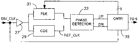
Figure 4 illustrates the basic elements of an
intelligent dynamic delay compensation circuit which
determines the number of fine delay steps required to
replace a coarse delay element to be switched out of the
main delay line such that the delay mismatch is reduced
to less than one fine delay step. This circuit allows
the DLL to track the system clock CLK by using high
resolution fine delay steps, while covering a range much
larger than that provided by the fine delay line, without
the inherent danger of switching jitter. It also allows
fine delay steps of high resolution to be employed
without compromising locking time, integrated circuit
area and power.
The clock CLK or a delayed version thereof
(DEL_DLK) is applied via a buffer 27 to two delay paths,
9
CA 02596269 2007-08-21
a reference coarse delay path which contains a coarse
delay element 29, and a variable fine delay path which
contains a controllable number of fine delay elements 31.
The outputs of the two paths are coupled to respective
inputs of a phase detector 33. Outputs of the phase
detector 33 are up and down control signals which result
from the phase comparison; these signals are applied to a
counter 35, which also receives the clock signal CLK or a
divided version of the clock. The counter 35 provides a
control signal for controlling the number of fine delay
elements in the fine delay path of the delay line of
Figure 3, which will be stable,when the delays of both
delay paths are substantially equal. This represents the
accurate number of fine delay steps which should be
substituted for one coarse delay element. The count of
the counter 35 at this point is output to the control 5
of the DLL described with reference to Figure 3. The
circuit of Figure 4 (or the more detailed preferred
circuit of Figure 5) is represented by element 25 of
Figure 3.
Since the delay elements in the compensation
circuit 25 of Figure 3 are manufactured simultaneously as
those of the delay lines 13 and 15, and are preferably
located on the chip close together, they will exhibit
substantially the same characteristics.
In a preferred embodiment of the present
invention the coarse delay element 29 is an RC based
delay well known.in the art driven by an inverter, and
has a delay of about 0.8ns. The fine delay element 31
consists of 32 fine steps, each of the form shown in
Figure 2, each step being about 25ps.
In the main delay line of Figure 3, preferably
four fine delay elements are used to form a fine delay
CA 02596269 2007-08-21
line 15 of +/- 64 fine steps, each element being
implemented using binary weighted capacitor based RC
delay elements. Without the compensation circuit, during
switching, one fine delay element or 32 fine steps are
substituted by a coarse delay element.
The phase detector samples the system CLK or
delayed CLK (DEL CLK) at the rising edge of CLK or
DEL CLK (the output of the coarse delay path 29) and
indicates by its output up and down signals whether the
DEL CLK is early or late with respect to REF CLK. The
phase detector can be any implementation of a meta-stable
hardened rising edge triggered D flip-flop.
The CNTR 35 is preferably a 6 bit up/down binary
counter, which is reset to half of its value,i.e. 32
steps. The counter is clocked from the input clock
DEL CLK and counts up or down depending on the output of
the phase detector. =
Figure 5 illustrates a preferred form of the
invention, in which two of the aforenoted fine delay
elements FDE1 and FDE2 (elements 31A and 31B) are shown
serially connected. The elements are selected by means
of a thermometer decoder 37 driven by the output of
counter 35.
The coarse delay path also includes additional
fine delay elements FD3 and FD4 (elements 39A and 39B)
which have intrinsic delays which are equal to the
minimum delay of the elements 31A and 31B respectively.
These are added because one coarse delay interval of a
coarse delay element 13 could be greater than that of one
nominal coarse delay element, and the additional fine
delay elements 39A and 39B add to the interval of CDE to
at least equal to the delay interval which is greater
than one nominal delay element.
11
CA 02596269 2007-08-21
In operation, the clock input is driven by
DEL CLK, a divided version of the main clock, to reduce
power consumption. The DEL CLK is then buffered by
buffer 27 and is delayed through the above-described two
delay paths. The fine delay elements 39A and 39B have
their control inputs set to 0, so that the path through
them includes only their intrinsic delay.
The fine delay path is comprised of the two fine
delay elements 31A and 31B which have their control
inputs fed by the counter 35 output. In this
configuration the DEL CLK is delayed by tCDE + 2 x
tFDE(0) through the coarse delay path, where tFDE(O) is
the intrinsic delay of a fine delay element, and tCDE is
the time delay of a coarse delay element.
DEL CLK is delayed by tFDE(I) + 2 x tFDE(O)
through the fine delay path, where I is the counter
output and can vary from 0 to 64.
The phase detector samples DEL CLK at the rising
edge of REF_CLK and indicates whether DEL CLK is late or
early with respect to REF_CLK. The counter uses the
phase detector's output to count up if DEL CLK is early
and down if DEL CLK is late. The output of the counter
is used by the fine delay elements FDEl and FDE2 (31A and
31B) to reduce the error on DEL CLK. Thus I is adjusted
by the above-described feedback mechanism so that tFDE(I)
+ 2 x tFDE(0) = tCDE + 2 x tFDE(0); or in other words,
until tFDE(I) = tCDE. This ensures that the maximum
error on DEL CLK is no more than tFDE(I), or
approximately 25ps.
Once the error has been reduced to less than one
fine delay element step, the counter counts one up and
one down to stay within the above error range. In this
state the circuit is in lock. Once in the locked state,
12
CA 02596269 2007-08-21
I is continually updated as the temperature and voltage
conditions change, thereby providing an accurate count
for the fine delay elements that ensures minimum mismatch
between the coarse delay and fine delay element delays
across process parameters and temperature and voltage
drifts.
The output of the counter 35 can be loaded in
parallel into another counter which can be implemented
within the control circuit 5 of Figure 3 and can be used
to control the entire fine delay line 15 in the main
delay line whenever there is an overflow condition and
switching between coarse and fine elements is required.
A control signal can be used to add I to the fine delay
line control output of this other counter by simply
loading I into the other counter or by subtracting I from
the other counter by loading 1's complement of I into the
other counter. This can be used to account for both
overflow and underflow conditions.
For example, if the main delay locked loop is
tracking by decreasing the delay and reaches an underflow
(all 0's) condition, it must switch out a coarse delay
element and add an equivalent amount of fine delay
controlled through a count in the other counter. Thus in
the all 0 or underflow condition I from the counter 35 is
added to the other counter by simply loading the count I
into the other counter. However, during overflow, the
other counter contains all l's and thus the counter 35
output I must be subtracted from all 1's to get the
desired operation. This subtraction from all l's is
simply achieved through the loading of l's complement of
I into the other counter.
While the above-described embodiments are digital
whereby counters are used to determine the compensated
13
CA 02596269 2007-08-21
fine delay to be used during switching, such compensation
can be achieved using other means. For example, a phase
accumulator can be used instead of the phase detector 33
to compensate the delay by using voltage controlled delay
elements. The error voltage achieved through this
implementation can then be added or subtracted from the
control voltage used to drive a voltage controlled delay
line.
In addition, the input drive conditions of the
two paths feeding the coarse and fine paths in the
structure of Figure 5 can be matched, and the output
loading conditions can be established to accurately model
the actual operating conditions of the coarse and fine
delay elements of the main DLL.
While the above embodiments have been described
using the DLL as the circuit to which they are applied in
order to reduce switching jitter, the concepts can be
used in other applications that involve tracking delays
with respect to any reference delay path. For example,
the invention can be used in clock recovery circuits, pin
timing tuners used in integrated circuit testers, etc.
A person understanding this invention may now
conceive of alternate embodiments and enhancements using
the principles described herein. All such embodiments
and enhancements are considered to be within the spirit
and scope of this invention as defined in the claims
appended hereto.
14