Note: Descriptions are shown in the official language in which they were submitted.
CA 02596996 2007-08-03
Process for the production of a multi-IaYer body and a multi-layer body
The invention concerns a process for the production of a multi-layer
body having a partially shaped first layer and a multi-layer body having a
replication layer and a first layer partially arranged on the replication
layer.
Such components are suitable as optical components or also as lens
systems in the field of telecommunications.
GB 2 136 352 A describes a production process for the production of
a sealing film provided with a hologram as a security feature. In that case
after the operation of embossing a diffractive relief structure a plastic film
is metallised over its full area and then demetallised in region-wise fashion
in accurate register relationship with the embossed diffractive relief
structure.
Demetallisation in accurate register relationship is costly and the
degree of resolution which can be achieved is limited by the adjustment
tolerances and the procedure employed.
EP 0 537 439 B2 describes processes for the production of a security
element with filigree patterns. The patterns are formed from diffractive
structures covered with a metal layer and surrounded by transparent
regions in which the metal layer is removed. It is provided that the outline
of the filigree pattern is introduced in the form of a depression into a metal-
coated carrier material, in that case at the same time the bottom of the
depressions is provided with the diffractive structures and then the
depressions are filled with a protective lacquer. Excess protective lacquer is
to be removed by means of a scraper blade.
After application of the protective lacquer, it is provided that the
metal layer is removed by etching in the unprotected transparent regions.
The depressions are between about i m and 5 m while the diffractive
structures can involve height differences of more than 1 m. That process
which, in repetition steps, requires adjustment steps for orientation in
accurate register relationship, fails when dealing with finer structures. In
addition continuous metallic regions covering an area are difficult to
1
CA 02596996 2007-08-03
implement as the 'spacers' are missing, for the operation of scraping off the
protective lacquer.
The object of the present invention is to provide a multi-layer body
and a process for the production of a multi-layer body, in which a layer
which has regions in which the layer is not present can be applied in
register relationship with a high level of accuracy and inexpensively.
In accordance with the invention that object is attained by a process
for the production of a multi-layer body having a partially shaped first
layer, wherein it is provided that a diffractive first relief structure with a
high depth-to-width ratio of the individual structure elements, in particular
with a depth-to-width ratio of > 0.3, is shaped in a first region of a
replication layer of the multi-layer body, and the first layer is applied to
the
replication layer in the first region and in a second region in which the
first
relief structure is not shaped in the replication layer, with a constant
surface density with respect to a plane defined by the replication layer,
and the first layer is partially removed in a manner determined by the first
structure, so that the first layer is removed in the first region but not in
the
second region or in the second region but not in the first region.
The object is further attained by a multi-layer body having a
replication layer and at least one first layer partially arranged on the
replication layer, wherein it is provided that a diffractive first relief
structure
with a high depth-to-width ratio of the individual structure elements, in
particular with a depth-to-width ratio of > 0.3, is shaped in a first region
of
the replication layer, the first relief structure is not shaped in the
replication
layer in a second region of the replication layer, and the partial
arrangement of the first layer is determined by the first relief structure so
that the first layer is removed in the first region but not in the second
region or in the second region but not in the first region.
The invention is based on the realisation that the special diffractive
relief structure in the first region influences physical properties of the
first
layer applied to the replication layer in that region such as transmission
properties, in particular transparency, or effective thickness of the first
layer, so that the physical properties of the first layer differ in the first
and
2
CA 02596996 2007-08-03
second regions. The first layer is now used as a kind of mask layer for
partial removal of the first layer itself or for partial removal of a further
layer. That affords the advantage, over the mask layers applied with
conventional processes, that that mask layer is oriented in accurate register
relationship without additional adjustment complication and expenditure.
The first layer is an integral component part of the structure which is
shaped in the replication layer. A lateral displacement between the first
relief structure and regions of the first layer with the same physical
properties does not occur. The arrangement of regions of the first layer
with the same physical properties is exactly in register relationship with the
first relief structure. Accordingly only the tolerances of that relief
structure
have an influence on the tolerances of the position of the first layer.
Additional tolerances do not arise. The first layer is a layer which
preferably
performs a dual function. On the one hand it implements the function of a
highly accurate mask layer, for example a highly accurate exposure mask
for the production procedure while on the other hand (at the end of the
production procedure) it forms a highly accurately positioned functional
layer, for example an OVD layer or a conductor track or a functional layer
of an electrical component, for example an organic semiconductor
component.
Furthermore it is possible to produce structured layers of very high
resolution by means of the invention. The degree of resolution which can be
achieved is approximately better by a factor of 100 than those which can
be attained by known demetallisation processes. As the width of the
structure elements of the first relief structure can be in the region of the
wavelength of visible light (between about 380 and 780 nm) but also below
same, it is possible to produce metallised pattern regions enjoying very fine
contours. That means that in this respect also great advantages are
achieved in comparison with the demetallisation processes used hitherto,
and it is possible with the invention to produce security elements with a
higher level of safeguard against copying and forgery than hitherto.
It is possible to produce lines and/or dots with a high level of
resolution, for example of a width or of a diameter respectively of less than
3
CA 02596996 2007-08-03
m, in particular to about 200 nm. Preferably levels of resolution in the
region of between about 0.5 m and 5 m, in particular in the region of
about 1 m, are achieved. In comparison, processes which involve
adjustment in register relationship make it possible to implement line
5 widths of less than 10 m, only at a very high level of complication and
expenditure.
The first layer can be a very thin layer of the order of magnitude of
some nm. The first layer applied with a uniform surface density, with
respect to the plane defined by the replication layer, is considerably thinner
in regions with a high depth-to-width ratio than in regions with a low
depth-to-width ratio.
The dimensionless depth-to-width ratio is a characteristic feature for
enlargement of the surface of preferably periodic structures, for example of
a sine-square configuration. The depth here is the spacing between the
highest and the lowest successive points of such a structure, that is to say
the spacing between a 'peak' and a 'trough'. The spacing between two
adjacent highest points, that is to say between two 'peaks', is referred to as
the width. Now, the higher the depth-to-width ratio, the correspondingly
steeper are the 'peak flanks', and the correspondingly thinner is the first
layer which is deposited on the 'peak flanks'. That effect is also observed in
the case of a rectangular structure with vertical 'peak' flanks. This however
can also involve structures to which this model cannot be applied. By way
of example, the situation may involve discretely distributed regions in line
form, which are only in the form of a 'trough', wherein the spacing between
two 'troughs' is a multiple greater than the depth of the 'troughs'. Upon
formal application of the above-specified definition the depth-to-width ratio
calculated in that way would be approximately zero and would not reflect
the characteristic physical condition. Therefore, in the case of discretely
arranged structures which are formed substantially only from a 'trough',
the depth of the 'trough' is to be related to the width of the 'trough'.
Such multi-layer bodies are suitable for example as optical
components such as lens systems, exposure and projection masks or as
security elements for safeguarding documents or ID cards, insofar as they
4
CA 02596996 2007-08-03
cover critical regions of the document such as a passport picture or a
signature of the owner or the entire document. They can also be used as
components or decoration elements in the field of telecommunications.
The multi-layer body can be a film element or a rigid body. Film
elements are used for example to provide documents, banknotes or the like
with security features. That can involve security threads for being woven
into paper or for being introduced into a card, which can be formed with the
process according to the invention with a partial demetallisation in perfect
register relationship with an OVD design.
It has further proven to be desirable if the multi-layer body is
arranged in the form of a security feature in a window of a value-bearing
document or the like. New security features with a particularly brilliant and
filigree appearance can be generated by means of the process according to
the invention. Thus it is possible for example to produce images which are
semi-transparent in the transillumination mode by forming a rastering of
the first layer. Furthermore it is possible for a first item of information to
be
rendered visible in such a window in the reflection mode and for a second
item of information to be rendered visible in the transillumination mode.
Advantageously rigid bodies such as an identity card, a base plate for
a sensor element or a housing shell portion for a cell phone can also be
provided with the optionally partially demetallised layers according to the
invention, which are in register relationship with functional structures or
with a diffractive design element. It can be provided that the replication
layer is introduced and structured directly with the injection molding tool or
by means of shaping with a die using UV lacquer.
Advantageous configurations of the invention are set forth in the
appendant claims.
= In accordance with a preferred embodiment of the invention first
regions in which the diffractive relief structure with a high depth-to-width
ratio is provided alternate with second regions in which there is provided an
optical active diffractive structure having a conventional, lower depth-to-
width ratio. By way of example the first relief structure in the first region
is
respectively of a depth of 5 m and a width of 2.5 m, that is to say a high
5
CA 02596996 2007-08-03
depth-to-width ratio of 2, and in the second region it is of a depth of 0.15
m and a width of 2.5 m, that is to say a low depth-to-width ratio of 0.06.
That makes it possible for the structuring of the first layer and/or
one or more further layers to be oriented in accurate register relationship
with the optical effects produced by the diffractive structures in the second
region, with a very small tolerance. In that respect, instead of a diffractive
structure, it is also possible to provide in the second region another
optically active microstructure or macrostructure, for example a micro-lens
raster. Security elements with a higher level of copying and forgery
protection can be produced by the highly accurate orientation, which can be
achieved by means of the invention, in respect of partially shaped layers of
a security element with optically active relief structures of the security
element.
In that way for example filigree patteriis such as guilloche patterns
can be produced, which are oriented exactly in relation to diffractive
structures which correspond to configurational motifs of a hologram or a
Kinegram .
The first layer is applied to the replication layer preferably by means
of sputtering, vapor deposition or spraying. In the sputtering operation, due
to the procedure involved, a directed application of material takes place so
that when applying material of the first layer by sputtering, in a constant
surface density with respect to the plane defined by the replication layer, to
the replication layer provided with the relief structure, the material is
deposited locally in differing thicknesses. Vapor deposition and spraying of
the first layer, by virtue of the operating procedure involved, preferably
also produces at least partially directed application of material.
In accordance with a preferred embodiment of the invention the first
layer is partially removed by a time-controlled etching process. The basic
starting point is the fact that relief structures with a high depth-to-width
ratio involve a markedly larger surface area than flat surfaces or surfaces
with relief structures which have a low depth-to-width ratio. The etching
p'rocess is terminated when the first layer is completely removed, or at
least the layer thickness is reduced, in the regions with a high depth-to-
6
CA 02596996 2007-08-03
width ratio. The first layer still covers the second layer when the first
layer
is already completely removed in the first region, by virtue of the different
physical properties, governed by the specific relief structure in the first
region, of the first layer in the first and second regions (smaller effective
thickness). By way of example lyes or acids can be provided as the etching
agents. It is however also possible to provide that the first layer is only
partially removed and the etching operation is interrupted as soon as a
predetermined degree of transmission or transparency is achieved. In that
way it is possible for example to produce security features which are based
on locally differing transmission or transparency.
If a multi-layer body with a for example vapor-deposited reflection
layer as the first layer is exposed to an etching medium which is
predominantly isotropic the reflection layer is already completely removed
in regions with a high depth-to-width ratio while in regions with a low
depth-to-width ratio there is still a residual layer present. If for example
aluminum is used as the reflection layer lyes such as NaOH or KOH can be
used as the isotropically acting etching agent. It is also possible to use
acid
media such as PAN (a mixture of phosphoric acid, nitric acid and water).
The reaction speed typically increases with the concentration of the
lye and temperature. The choice of the process parameters depends on the
reproducibility of the procedure and the resistance of the multi-layer body.
If the first layer is to be opaque after the etching operation in the
second region then the optical density is preferably selected there to be >
1.5. In order to compensate for the removal of the first layer, which also
occurs in the isotropic etching operation in the second regions with a low
depth-to-width ratio, it is therefore necessary to start with a
correspondingly higher optical density. The compensation can contribute a
multiple of the optical density envisaged, depending on the respective
differences in the depth-to-width ratio. If for example an Al layer is applied
by vapor deposition as the first layer which in a second flat region is
opaque or has an optical density of 6 and there provides a metallic mirror,
and if the Al layer is correspondingly etched, it is possible to achieve after
the etching operation in the second region an opaque layer with properties
7
CA 02596996 2007-08-03
which are still specularly reflecting and with an optical density of 2, while
the AI layer has already been completely etched away in adjacent first
regions which are provided with a relief structure with a high depth-to-
width ratio.
Influencing factors when etching with lye are typically the
composition of the etching bath, in particular the concentration of etching
agent, the temperature of the etching bath and the afflux flow conditions of
the layer to be etched in the etching bath. Typical parameter ranges in
respect of the concentration of the etching agent in the etching bath are in
the region of between 0.1% and 10% and in respect of temperature in the
region of between 20 C and 80 C.
The etching operation for the first layer can be electrochemically
assisted. The etching operation is intensified by the application of an
electrical voltage. The action is typically isotropic so that the structure-
dependent increase in surface area additionally intensifies the etching
effect. Typical electrochemical additives such as wetting agents, buffer
substances, inhibitors, activators, catalysts and the like in order to remove
for example oxide layers can promote the etching procedure.
During the etching procedure depletion of etching medium or
enrichment in respect of the etching products can occur in the interface
layer in relation to the first layer, whereby the etching speed is slowed
down. Forced mixing of the etching medium, possibly by the production of
a suitable flow or ultrasound excitation, improves the etching
characteristics.
The etching procedure can further involve a temperature profile in
respect of time in order to optimise the etching result. Thus etching can be
effected in the cold condition at the beginning and warmer with an
increasing period of operation. That is preferably implemented in the
etching bath by a three-dimensional temperature gradient, in which case
the multi-layer body is drawn through an elongate etching bath with
different temperature zones.
The last nanometers of the first layer can prove to be relatively
stubborn and resistant to etching in the etching procedure. Therefore, slight
8
CA 02596996 2007-08-03
mechanical assistance for the etching process is advantageous for removing
the remains of the last layer. The stubbornness is based on a possibly
slightly different composition in respect of the first layer, presumably by
virtue of interface layer phenomena when the first layer is formed on the
replication layer. In that case the last nanometers of the first layer are
preferably removed by a wiping process by the multi-layer body being
passed over a roller covered with a fine cloth. The cloth wipes off the
remains of the first layer without damaging the multi-layer body.
It will be appreciated that the process according to the invention can
be readily combined with structuring or etching processes which are
already known and which usually operate with masks in the form of
structured etching resist masks or washing masks.
Besides wet-chemical etching processes use of dry etching processes
such as plasma etching is also advantageous for partial complete or part-
wise removal of the first layer.
In addition laser ablation has proved its worth for removing the first
layer. A first layer which for example is in the form of a metallic reflection
layer is in that case removed region-wise by direct irradiation with a
suitable laser by making use of the absorption characteristics of the
different relief structures in the different regions of the multi-layer body.
In the case of structures with a high depth-to-width ratio and in
particular relief structures in which the typical spacing between two
adjacent raised portions is less than the wavelength of the incident light,
so-called zero order structures, a large part of the incident light can be
absorbed, even if the degree of reflection of the reflection layer, in a
region
involving mirror reflection, is high. The reflection layer is irradiated by
means of a focused laser beam, in which case the laser radiation is
absorbed to an increased extent and the reflection layer is correspondingly
increased in temperature in the strongly absorbent regions which have the
above-mentioned structures with a high depth-to-width ratio. With high
levels of energy input the reflection layer can locally spall off, in which
case
removal or ablation of the reflection layer or coagulation of the materiai of
the reflection layer occurs. If energy input by the laser is effected only
over
9
CA 02596996 2007-08-03
a short period of time and the effect of thermal conduction is thus only
slight, ablation or coagulation occurs only in the regions which are pre-
defined by the relief structure.
Influencing factors in laser ablation are the configuration of the relief
structure (period, depth, orientation, profile), the wavelength, polarisation
and angle of incidence of the incident laser radiation, the duration of the
at;tion (time-dependent power) and the local dose of laser radiation, the
properties and the absorption characteristics of the first layer, as well as
the first layer possibly having further layers covering it above it or below
it.
Inter alia Nd:YAG lasers have proven to be suitable for the laser
treatment. They emit at about 1064 mm and are preferably also operated
in a pulsed mode. It is further possible to use diode lasers. The wavelength
of the laser radiation can be altered by means of a frequency change, for
example frequency doubling.
The laser beam is guided over the multi-layer body by means of a
so-called scanning device, for example by means of galvanometric mirrors
and a focusing lens. Pulses of a duration in the region of nanoseconds to
microseconds are emitted during the scanning operation and lead to the
above-described ablation or coagulation of the first layer, as is
predetermined by the structure. The pulse durations are typically below
milliseconds, advantageously in the region of a few microseconds or less. It
is thus certainly also possible to use pulse durations of nanoseconds to
femtoseconds. Precise positioning of the laser beam is not necessary as the
procedure is self-referencing. The procedure is preferably further optimised
by a suitable choice in respect of the laser beam profile and overlapping of
adjoining pulses.
It is however equally possible to control the path of the laser over
the multi-layer body in register relationship with relief structures disposed
in the replication layer so that only regions with the same relief structure
are irradiated. For example camera systems can be used for such control.
Instead of a laser which is focused on to a point or a line it is also
possible to use areal radiating devices which emit a short, controlled pulse
such as for example flash lights.
CA 02596996 2007-08-03
The advantages of the laser ablation process include inter alia the
fact that the partial removal of the first layer, in register relationship
with a
relief structure, can also take place if it is covered on both sides with one
or
more further layers which are transmissive in respect of the laser radiation,
and it is thus not directly accessible to etching media. The first layer is
only
broken up by the laser. The material of the first layer breaks off again in
the form of small conglomerates or small balls which are not optically
visible to the viewing person and which only immaterially influence the
transparency in the irradiated region.
Residues from the first layer which have still remained on the
replication layer after the laser treatment can optionally be removed by
means of a subsequent washing procedure if the first layer is directly
accessible.
In accordance with a further preferred embodiment of the invention
the first layer is applied to the replication layer in a surface density which
is
so selected that the transparency of the first layer in the first region is
increased by the first relief structure with respect to the transparency of
the first layer in the second region.
The opaque first layer which is produced with transparent regions in
that way can also be altered by further process steps or used as a mask for
producing further layers. For example it can be provided that the first layer
is removed in the transparent regions. That can be implemented by an
etching or ablation process as described hereinbefore. Thus for example in
ah intermediate step an etching mask is produced as a 1:1 copy from the
first layer, covering the regions of the first layer, which are to be
protected
from the action of the etching agent.
The multi-layer body according to the invention can have further
regions which are produced with conventional processes, for example to
produce decorative color effects which extend over regions or over the
entire multi-layer body.
The production of the first layer is not bound to a specific material.
The first layer however should advantageously be opaque, outside
11
CA 02596996 2007-08-03
transparent regions, if the time-controlled etching process described
hereinbefore is not provided for setting a defined level of transmission.
Transparent materials can be colored in order to make them opaque.
Preferably however it can be provided that the first layer is produced from
a metal or a metal alloy. The opacity of the metallic layer can in that case
be adjusted by the amount of material applied per unit of surface area, by
the nature of the metal and by the relief structure in the first region.
Metallic first layers can be reinforced again by gaivanisation for
example in order to increase the reflection capability or the conductivity of
the layer which has remained. It is possible in that way to produce
connecting lines for electronic circuits or electronic components such as
antennae and coils of high electrical quality.
It can be provided that the first metallic layer is reinforced by the
application of the same metal. It can however also be provided that the
first layer is produced from a first metal or a first metal alloy and a second
metal is applied for reinforcement purposes. Thus by way of example it is
possible to produce a layer which is built up layer-wise from different
metals or metal alloys. That can involve for example a miniaturised bimetal
element.
It can however also be provided that the first layer is built up layer-
wise from partial layers of different metals or metal. alloys in order to
utilise
the different physical and/or chemical properties of the partial layers for
implementing the process steps and/or for producing the properties of the
final product. By way of example the first layer can be built up from
aluminum and chromium, in which case the aluminum which is a good
reflector can improve the optical properties of the final product and the
chromium which is chemically more resistant permits the etching
procedures to be of an advantageous nature.
Layer-wise construction of the first layer is not restricted to metallic
layers. This can also involve dielectric layers or polymer layers. In that
respect it can also be provided that successive layers are made up from
differing material and/or of differing thickness for example to produce the
known color change effects on thin layers.
12
CA 02596996 2007-08-03
The polymer layer can be an organic semiconductor layer which can
be a constituent part of an organic semiconductor component or an organic
circuit. Such polymer layers can be produced in the form of fluids in the
broadest sense and applied for example by means of printing processes.
Because application of the polymer layer does not have to be effected in
accurate register relationship in accordance with the process of the
invention, it can be particularly inexpensively carried into effect.
It can be provided that the replication layer is in the form of a
photoactive washing mask which is exposed through the first layer and
activated and that the exposed regions of the washing mask and the
regions of the first layer arranged there on the washing mask are removed.
Washing masks are distinguished by being environmentally friendly
as for example it is also possible to use water as a solvent for removing the
exposed regions of the washing mask. Care is to be taken to ensure
however that the washing mask is sufficiently permanent in order not to
limit the multi-layer body formed with the washing mask, in terms of its
service life and/or reliability. It can be advantageous if removal of the
exposed regions of the washing mask at the same time also entails removal
of the surface structure produced there, with a high depth-to-width ratio.
That can be advantageous in regard to introducing a second layer into the
washed-out regions of the first layer.
As a further process it can be provided that a photosensitive layer is
applied to the first layer. The thickness of the photosensitive layer can be
in
the region of between 0.05 m and 50 m, advantageously in the region of
between 0.1 m and 10 m. That can involve a photoresist, as is known
from the semiconductor industry. The photoresist can be a fluid which can
be applied by means of a coating installation. Alternatively a dry thin
photopolymer layer can also be applied by lamination.
The photoresist can be in the form of a positive photoresist or a
negative photoresist. The positive photoresist is a photoresist in which
exposed regions are soluble in a developer. In a corresponding fashion the
negative photoresist is a photoresist in which unexposed regions are
13
CA 02596996 2007-08-03
soluble in the developer. It is possible in that way to produce multi-layer
bodies which are different, with a first layer.
By way of example when using a negative photoresist the first layer
can be in the form of a metallic layer which is removed by etching in the
unexposed regions and is then replaced by a second layer. For that purpose
firstly the second layer is applied over the full surface area and then
removed in the exposed regions together with the photoresist which has
remained. The first layer can now be galvanically reinforced. In that way
the partially transparent first layer can be converted into an opaque first
layer which is embedded in a transparent surrounding area. In this case
also association of the regions formed in that way, in accurate register
relationship, is retained.
The choice of the appropriate photoresist can depend on the nature
of the first layer used, the wavelength of the light source and the desired
resolution. It can advantageously be provided that the light source emits
UV light in the range of between 300 nm and 400 nm.
In regard to the choice of the light source, besides the spectral
sensitivity of the photoresist, the transmission of the layers arranged over
the photoresist, in particular that of the first layer, is also to be taken
into
consideration.
As regards now the development of the exposed photosensitive
layer, an etching characteristic with an abrupt change can advantageously
be provided when using a positive photoresist. The term etching
characteristic is used to denote here the dependency of the etching rate,
that is to say the removal of the exposed photosensitive layer per unit of
time, on the energy density which acts on the photosensitive layer due to
the exposure effect.
Subsequent to development of the photosensitive layer it can be
used as an etching mask for the first layer. The first layer can consequently
be removed by the action of the etching agent in the regions in which the
photosensitive layer is removed by development.
In place of the photosensitive layer it is also possible to provide a
photoactivatable layer. Such a layer can be altered by exposure in such a
14
CA 02596996 2007-08-03
way that it forms an etching agent in the exposed regions and in that way
can dissolve away the first layer.
It can also be provided that, in place of the photosensitive layer, an
absorption layer is applied, which for example absorbs laser light and in
that way is thermally destroyed in the regions irradiated with laser light.
The absorption layer which is irradiated with laser light now forms the
etching mask for removal of the regions of the first layer, which are
transmissive for the laser light. The absorption layer however can also
involve the first layer itself. By way of example, a relatively thick,
suitably
structured aluminum layer absorbs over 90% of the incident laser light, in
which respect absorption can be wavelength-dependent. Structures which
have only few diffraction orders for the incident laser light, that is to say
in
which for example the spacing between adjacent troughs is less than the
wavelength of the incident laser light, are particularly suitable for laser
ablation. It can be provided that a second layer is applied in the regions in
which the first layer is removed. That can involve for example a colored
layer or an electrochromic layer. Colored patterns or display elements can
be produced in that fashion.
A preferred embodiment of the invention provides that the second
layer can be applied over the full surface area involved subsequently to
etching of the first layer. Thereupon the residues of the etching mask are
removed, in which case the second layer is removed at the same time with
the etching mask in those regions in which the etching mask covers the
first layer. In that way the second layer is applied in accurate register
relationship to the regions of the multi-layer body in which the first layer
is
removed.
Colored regions can also be produced in accordance with the process
described hereinafter. A multi-layer body with a partial first layer of metal
is produced by means of the process according to the invention, wherein
the first layer in the first region is radiation-transmissive, for example for
UV radiation, and serves as a mask for a colored photoresist layer applied
to the first layer. Coloring of the photoresist layer can be effected in that
case by means of pigments or soluble dyestuffs.
CA 02596996 2007-08-03
Then the photoresist is exposed through the first layer, by means for
example of UV radiation, and hardened or destroyed in the first regions,
depending on whether it is a positive or the negative resist. In that case
positive and negative resist layers can also be applied in mutually
juxtaposed relationship and exposed at the same time. In that case the
first layer serves as a mask and is preferably arranged in direct contact
with the photoresist so that precise exposure can be effected.
Finally, when developing the photoresist, the regions which have not
been hardened are washed off or the destroyed regions are removed.
Depending on the respective photoresist used the developed colored
photoresist is now either present precisely in the regions in which the first
layer is transparent or opaque in relation to the UV radiation. In order to
increase the resistance of the photoresist layer which has remained and
which is structured in accordance with the first layer, regions which have
remained are preferably post-hardened after the development operation.
I Finally the first layer which is used as the mask can be removed by a
further etching step to such an extent that the multi-layer body only has a
highly resolved 'color print' of photoresist for the viewing person, but is
otherwise transparent.
Advantageously, display elements of high resolution can be produced
in that way. Without departing from the scope of the invention it is possible
for differently colored display elements to be applied in accurate register
relationship and for them to be arranged for example in an image dot
raster. As different inuiti-layer bodies can be produced with an initial
layout
in respect of the first layer, by a procedure whereby for example different
exposure and etching processes are combined together or are carried out in
succession, positioning in accurate register relationship of the successively
applied layers is possible when using the process according to the
invention, in spite of an increase in the process steps.
Rastering of the first layer is also possible to the effect that, beside
raster elements which are underlaid with a reflection layer and which have
possibly different diffractive diffraction structures, there are provided
raster
elements which represent transparent regions without a reflection layer. In
16
CA 02596996 2007-08-03
that respect amplitude-modulated or area-modulated rastering can be
selected as the rastering effect. Attractive optical effects can be achieved
by a combination of such reflective/diffractive regions and non-reflective,
transparent - under some circumstances also diffractive - regions. If such
a raster image is arranged for example in a window in a value-bearing
document, a transparent raster image can be perceived in the
transillumination mode. In the incident illumination mode that raster image
is visible only in a given angular range in which no light is
diffracted/reflected by the reflecting surfaces. It is further possible for
such
elements to be used not only in a transparent window but also to be
applied to a colored imprint. In a given angular range the colored imprint is
visible for example in the form of the raster image while in another angular
range it is not visible by virtue of the light which is reflected by the
diffraction structures or other (macro-)structures. Furthermore it is also
possible for a plurality of outgoing reflection regions which decrease in
their
reflectivity to be produced by a suitably selected rastering effect.
Because regions of stepped transparency can be produced by a
variation in the depth-to-width ratio in the first layer, it can also be
provided that the first layer is removed in subsequent steps, that is to say
firstly the regions in which the first layer is at its thinnest are exposed
and
a second layer is applied there, thereafter the regions of the first layer
which are of the next following thickness are removed and a third layer is
applied there, and those steps are repeated until new layers are applied in
all regions of the first layer with a high depth-to-width ratio. This can
involve optically hardenable layers which are not subjected to initial
dissolution after hardening by an etching agent.
In that way it is also possible for regions to be arranged in accurate
register relationship in non-metallic layers. Thus for example the first layer
can be formed from a dielectric with a first refractive index and the second
layer can be formed from a dielectric with a second refractive index. In that
way the second layer can form a pattern in the first layer or vice-versa. The
pattern can be perceived in incident light by virtue of the differing light
r'Llfraction of the two layers. Such a pattern is optically less striking than
a
17
CA 02596996 2007-08-03
pattern produced by metallic layers and can therefore be preferred as a
security feature for passes or other security documents. It can appear to
the viewing person for example as a transparent pattern of green or red.
Furthermore it is also possible to construct by means of the invention
regions involving different metallic and non-metallic layers which
respectively produce a differing thin film system with different optical
properties, for example different viewing angle-dependent color shift
effects. A thin film layer system is distinguished in principle by an
interference layer structure which produces viewing angle-dependent color
shifts. It can be made up in the form of a reflective element, with for
example a highly reflecting metal layer, or a transmissive element with a
transparency optical separation layer in relation to the individual layers.
The basic structure of a thin film layer system has an absorption layer
(preferably with between 30 Io and 65 Io transmission), a transparency
spacer layer in the form of a color change-producing layer (for example X/4
or X/2 layer) and a metal layer as a reflecting layer or an optical separation
layer. It is further possible for a thin film layer system to be made up from
a succession of high-refraction and low-refraction layers. The greater the
number of layers, the correspondingly easier is it possible to adjust the
wavelength for the color change. Examples of usual layer thicknesses in
respect of the individual layers of a thin film layer system and examples of
materials which can be used in principle for the layers of a thin film layer
system are disclosed by way of example in WO 01/03945, page 5, line 30
through page 8, line 5.
It can further be provided that the carrier layer is in the form of a
repiication layer.
The process according to the invention can be continued for
application of further layers in accurate register relationship. By way of
example a fourth layer can be applied to the layers arranged on the
replication layer, in a surface density, that the transparency of the fourth
layer in the first region is increased by the first relief structure with
respect
to the transparency of the fourth layer in the second region, and that the
fourth layer is perforated in a manner determined by the first relief
18
CA 02596996 2007-08-03
structure so that the fourth layer is perforated in the first region or in the
second region but not in the second region or in the first region
respectively. That fourth layer is thus in the form of a mask layer, like the
first layer, so that the above-described process steps can be repeated in
order to constitute the multi-layer body with further layers which are
perforated in accurate register relationship. Transmission of the structured
first layer can also be used for register-related structuring of the fourth
layer. In that way it is possible for example to produce organic components
and circuits, besides security elements.
It can also be provided that the succession of removal of material
and the association with the structures in the first and second regions is so
selected that regions are produced, in which different diffractive structures
are interlaced with each other. This may involve for example a first
Kinegram and a second Kinegram which have a different depth-to-width
ratio and which are arranged in front of a background. In that example it
can be provided that a vapor-deposited copper layer is removed only in the
region of the first Kinegram , then aluminum is applied by vapor deposition
over the entire surface area and removed in the background regions by
suitable process implementation. That produces two designs which are
partially metallised in register relationship and which differ in the metal
layer which faces towards the viewing person. In order to achieve such
effects it is possible to use differences in the transmission properties of
the
above-mentioned regions, which are produced by polarisation effects
and/or wavelength dependencies and/or dependencies on the angle of
incidence of the light.
The relief structures introduced into the replication layer can also be
so selected that they can serve for orientation of liquid crystal (polymers).
Thus in that case the replication layer and/or the first layer can be used as
an orientation layer for liquid crystals. For example structures in groove
form are introduced into such orientation layers, wherein the liquid crystals
are oriented in relation to such structures before they are fixed in their
orientation in that position by crosslinking or in some other fashion. It can
be provided that the crosslinked liquid crystal layer forms the second layer.
19
CA 02596996 2007-08-03
The orientation layers can have regions in which the orientation
direction of the structure constantly changes. If a region formed by means
of such a diffractive structure is viewed through a polariser with for
example a rotating direction of polarisation, various clearly discernible
security features, for example motion effects, can thus be produced by
virtue of the linearly changing direction of polarisation of the region. It
can
also be provided that the orientation layer has diffractive structures for
orientation of the liquid crystals, which are locally differently oriented so
that the liquid crystals when considered under polarised light represent an
item of information such as for example a logo.
The invention is described in greater detail with reference to the
drawings in which:
Figure 1 shows a diagrammatic view in section of a first embodiment
of a multi-layer body according to the invention,
Figure 2 shows a diagrammatic view in section of the first production
stage of the multi-layer body of Figure 1,
Figure 3a shows a diagrammatic view in section of the second
production stage of the multi-layer body of Figure 1,
Figure 3b shows a view on an enlarged scale of a portion IIIb from
Figure 3a,
Figure 4 shows a diagrammatic view in section of the third
production stage of the multi-layer body of Figure 1,
Figure 5 shows a diagrammatic view in section of the fourth
production stage of the multi-layer body of Figure 1,
Figure 5a shows a diagrammatic view in section of a modified
configuration of the production stage shown in Figure 5,
Figure 5b shows a diagrammatic sectional view of the production
stage following that shown in Figure 5a,
Figure 6 shows a diagrammatic view in section of the fifth production
stage of the multi-layer body of Figure 1,
Figure 7 shows a diagrammatic view in section of the sixth
production stage of the multi-layer body of Figure 1,
CA 02596996 2007-08-03
Figure 8 shows a diagrammatic view in section of the seventh
production stage of the multi-layer body of Figure 1,
Figure 9 shows a diagrammatic view in section of the fifth production
stage of a second embodiment of the multi-layer body of Figure 1,
Figure 10 shows a diagrammatic view in section of the sixth
production stage of a second embodiment of the multi-layer body of Figure
1,
= Figure 11 shows a diagrammatic view in section of the seventh
production stage of a second embodiment of the multi-layer body of Figure
1,
Figure 12 shows a diagrammatic view in section of the eighth
production stage of a second embodiment of the multi-layer body of Figure
1,
Figure 13 shows a diagrammatic view in section of a second
embodiment of a multi-layer body according to the invention,
Figures 14a through 14d show diagrammatic views in section of the
production steps of a third embodiment of a multi-layer body according to
the invention,
Figure 15 shows a schematic diagram of etching rates of a
photosensitive layer, and
= Figure 16 shows an example of use of a multi-layer body according
to the invention.
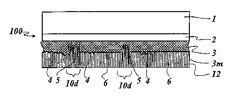
Figure 1 shows a multi-layer body 100 in which arranged on a carrier
film 1 are a functional layer 2, a replication layer 3, a metallic layer 3m
and
an adhesive layer 12. The functional layer 2 is a layer which predominantly
serves to enhance the mechanical and chemical stability of the multi-layer
body but which can also be designed in known manner to produce optical
effects. It can however also be provided that that layer is omitted and the
replication layer 3 is disposed directly on the carrier film 1. It can further
be
provided that the carrier film 1 itself is in the form of a replication layer.
The multi-layer body 100 can be a portion of a transfer film, for
example a hot stamping film, which is applied to a substrate by means of
the adhesive layer 12. The adhesive layer 12 can be a melt adhesive which
= 21
CA 02596996 2007-08-03
melts under the effect of heat and permanently joins the multi-layer body
to the surface of the substrate.
The carrier film 1 can be in the form of a mechanically and thermally
stable film comprising PET.
Regions involving different structures can be shaped into the
replication layer 3 by means of known processes. In the illustrated
embodiment these involve regions 4 having diffractive structures, that is to
say with a comparatively low depth-to-width ratio of the structure
elements, regions 5 with a high depth-to-width ratio of the structure
elements, and reflecting regions 6.
The metallic layer 3m disposed on the replication layer 3 has
demetallised regions 10d which are arranged in coincident relationship with
the diffractive structures 5. The multi-layer body 100 appears transparent
or partially transparent in the regions 10d.
Figures 2 through 8 now show the production stages of the multi-
layer body 100. The same components as in Figure 1 are denoted by the
same references.
Figure 2 shows a multi-layer body 100a in which the functional layer
2 and the replication layer 3 are arranged on the carrier film 1.
The replication layer 3 is structured in its surface by known
processes such as for example hot stamping.The replication layer 3 can be
a UV hardenable replication lacquer which is structured for example by a
replication roller. The structuring however can also be produced by UV
radiation through an exposure mask. In that way the regions 4, 5 and 6
can be shaped into the replication layer 3. The region 4 can be for example
the optically active regions of a hologram or a Kinegram .
Figure 3a now shows a multi-layer body 100b which is formed from
the multi-layer body 100a in Figure 2, by a procedure whereby the metallic
layer 3m is applied to the replication layer 3 with a uniform surface density,
for example by sputtering. In this embodiment the metallic layer 3m
involves a layer thickness of some 10 nm. The layer thickness of the
metallic layer 3m can preferably be so selected that the regions 4 and 6
involve a low level of transmission, for example between 10% and 0.001%,
22
CA 02596996 2007-08-03
that is to say an optical density of between i and 5, preferably between 1.5
and 3. Accordingly the optical density of the metallic layer 3m, that is to
say the negative decadic logarithm of transmission, is between i and 3 in
the regions 4 and 6. It can preferably be provided that the metallic layer
3m involves an optical density of between 1.5 and 2.5. The regions 4 and 6
therefore appear to be opaque or reflecting to the eye of the person
viewing them.
The metallic layer 3m in contrast is of reduced optical density in the
region 5. The responsibility for that lies with the increase in surface area
in
that region because of the high depth-to-width ratio of the structure
elements and the thickness which is reduced thereby of the metallic layer.
The dimension-less depth-to-width ratio is a characterising features for the
increase in surface area of preferably periodic structures. Such a structure
forms 'peaks' and 'troughs' in a periodic succession. The spacing between a
'peak' and a 'trough' is referred to here as the depth while the spacing
between two 'peaks' is referred to as the width. Now, the higher the depth-
to-width ratio, the correspondingly steeper are the 'peak flanks' and the
correspondingly thinner is the metallic layer 3m deposited on the 'peak
flanks'. That effect is also to be observed when the situation involves
discretely distributed 'troughs' which can be arranged relative to each other
at a spacing which is a multiple greater than the depth of the 'troughs'. In
such a case the depth of the 'trough' is to be related to the width of the
'trough' in order to correctly describe the geometry of the 'trough' by
specifying the depth-to-width ratio.
Figure 3b now shows in detail the thickness change effect in respect
of the metal layer 3m, which is responsible for affording transparency.
Figure 3b is a diagrammatic view in section of an enlarged portion
IIib from Figure 3a. The replication layer 3 has a relief structure 5h with a
high depth-to-width ratio in the region 5 and a relief structure 6n with a
depth-to-width ratio of equal to zero in the region 6. Arrows 3s identify the
direction of application of the metal layer 3m which can be applied by
sputtering, as described hereinbefore. The metal layer 3m is formed with
the nominal thickness to in the region of the relief structure 6n and with the
23
CA 02596996 2007-08-03
thickness t which is less than the nominal thickness to, in the region of the
relief structure 5t. In that respect the thickness t is to be interpreted as a
mean value for the thickness t is in dependence on the angle of inclination
of the surface of the relief structure 5t with respect to the horizontal. That
angle of inclination can be described mathematically by the first derivative
of the function of the relief structure 5t.
If therefore the angle of inclination is equal to zero, the metal layer
3m is deposited with the nominal thickness to, while if the magnitude of the
angle of inclination is greater than zero, the metal layer 3m is deposited
with the thickness t, that is to say with a smaller thickness than the
nominal thickness to.
It is also possible to achieve transparency for the metal layer by
relief structures which have a complex surface profile with raised portions
and recesses of differing height. Surface profiles of that kind can also
involve stochastic surface profiles. In that case, transparency is generally
attained if the mean spacing of adjacent structure elements is less than the
mean profile depth of the relief structure and adjacent structure elements
are spaced from each other at less than 200 m. Preferably in that respect
the mean spacing of adjacent raised portions is selected to be less than 30
m so that the relief structure 5t is a specific diffractive relief structure.
In terms of the configuration of transparent regions it is important
for the individual parameters to be known in terms of their dependencies
and appropriately selected. A viewing person already perceives a region as
being fully reflecting if 85% of the incident light is reflected, and already
perceives a region as being transparent if less than 20% of the incident
light is reflected, that is to say more than 80% is transmitted. Those values
can vary in dependence on the background, illijmination and so forth. In
that respect an important part is played by the absorption of light in the
metal layer. By way of example chromium and copper reflect much less
under some circumstances. That can signify that only 50% of the incident
light is reflected, in which case the degree of transparency is less than i%.
Table 1 shows the ascertained degree of reflection of metal layers of
Ag, Al, Au, Cr, Cu, Rh and Ti, arranged between plastic films (refractive
24
CA 02596996 2007-08-03
index n = 1.5) at a light wavelength x = 5S0 nm. In this case the thickness
ratio s is formed as the quotient of the thickness t of the metal layer, which
is required for the degree of reflection R = 80% of the maximum RMa, and
the thickness required for the degree of reflection R = 20% of the
maximum RMax.
Metal RMax t for 80% t for 20% h/d
RMax RM
Ag 0.944 31 nm 9 nm 3.4 1.92
Al 0.886 12 nm 2.5 nm 4.8 2.82
Au 0.808 40 nm 12 nm 3.3 1.86
Rh 0.685 18 nm 4.5 nm 4.0 2.31
Cu 0.557 40 nm 12 nm 3.3 1.86
Cr 0.420 18 nm 5 nm 3.6 2.05
Ti 0.386 29 nm 8.5 nm 3.3 1.86
Table i
From the point of view of heuristic consideration silver and gold (Ag
and Au), as can be seen, have a high maximum degree of reflection RMax
and require a relatively small depth-to-width ratio to produce transparency.
Aluminum (Al) admittedly also has a high maximum degree of reflection
RMax, but it requires a higher depth-to-width ratio. It can preferably
therefore be provided that the metal layer is formed from silver or gold. It
can however also be provided that the metal layer is formed from other
metals or from metal alloys.
Table 2 now shows the calculation results obtained from strict
diffraction calculations for relief structures with different depth-to-width
ratios, which are in the form of linear, sinusoidal gratings with a grating
spacing of 350 nm. The relief structures are coated with silver of a nominal
thickness to = 40 nm. The light which impinges on the relief structures is of
the wavelength k = 550 nm (green) and is TE-polarised or TM-polarised.
CA 02596996 2007-08-03
Depth- Grating Depth Degree of Degree of Degree of Degree of
to-width spacing in nm reflection transparency reflection transparency
ratio in nm (OR) TE 0T TE (OR) TM (OT) TM
0 350 0 84.5% 9.4% 84.5% 9.4%
0.3 350 100 78.4% 11.1% 50.0% 21.0%
0.4 350 150 42.0% 45.0% 31.0% 47.0%
1.1 350 400 2.3% 82.3% 1.6% 62.8%
2.3 350 800 1.2% 88.0% 0.2% 77.0%
Table 2
As was found, in particular the degree of transparency apart from the
depth-to-width ratio is dependent on the polarisation of the radiated light.
That dependency is shown in Table 2 for the depth-to-width ratio d/h =
1.1. It can be provided that that effect is put to use for the selective
f6rmation of further layers.
It was further found that the degree of transparency or the degree of
reflection of the metal layer 3m with the relief structure 5t (see Figure 3b)
is wavelength-dependent. That effect is particularly highly pronounced for
TE-polarised light.
It was further found that the degree of transparency decreases if the
angle of incidence of the light differs from the normal angle of incidence,
that is to say the degree of transparency decreases if the light is not
perpendicularly incident. That signifies that the metal layer 3m can be
transparent than in the region of the relief structure 5t, only in a
restricted
cone of incidence of the light. It can therefore be provided that the metal
layer 3m is opaque when viewed inclinedly, in which respect that effect can
also be used for the selective formation of further layers.
= Figure 4 shows a multi-layer body 100c formed from the multi-layer
body 100b shown in Figure 3a and a photosensitive layer S. This can be an
organic layer which is applied by conventional coating processes such as
intaglio printing in fluid form. It can also be provided that the
photosensitive layer is applied by vapor deposition or is applied by
lamination in the form of a dry film.
The application can be over the entire surface area. It is however
also possible to provide for application in partial regions, for example in
26
CA 02596996 2007-08-03
regions arranged outside the above-mentioned regions 4 through 6. This
can involve regions which have to be arranged only relatively coarsely in
register relationship with the design, for example decorative graphic
representations such as for example random patterns or patterns formed
from repeated images or texts.
Figure 5 now shows a multi-layer body 100d which is formed by
exposure of the multi-layer body 100c in Figure 4 through the carrier film
1. UV light 9 can be provided for the exposure operation. Because now, as
described hereinbefore, the regions S with a high depth-to-width ratio are
transparent the UV irradiation operation produces in the photosensitive
layer 8 regions 10 which have been greatly exposed and which differ from
less exposed regioris 11, in terms of their chemical properties. The regions
10 and 11 can differ for example by the solubility of the photosensitive
layer arranged there in solvents. In that way the photosensitive layer 8 can
be "developed" after the exposure operation with UV light, as is further
shown in Figure 6.
= Although a depth-to-width ratio of > 0.3 is advantageously provided
in the regions 5 and the thickness of the metallic layer 3m is
advantageously so selected that the regions 5 are at least partially
transparent, the process according to the invention can always be used if a
difference in optical density, which is sufficient for processing of the
photosensitive layer, is provided between the regions with a high depth-to-
width ratio and the other regions. There is therefore no need for the
metallic layer 3m to be so thin that the regions 5 appear transparent when
considered visually. A relatively low overall transmission of the vapor-
deposited carrier film can be compensated by an increased exposure dose
in respect of the photosensitive layer 8. It is further to be borne in mind
that exposure of the photosensitive layer is typically provided in the near
UV range so that the visual viewing impression is not crucial in terms of
a5sessing transmission.
Figures 5a and 5b show a modified embodiment. The photosensitive
layer 8 shown in Figure 5 is not provided in the multi-layer body 100d' in
Figure 5a. Instead there is a replication layer 3' which is a photosensitive
27
CA 02596996 2007-08-03
washing mask. The multi-layer body 100d' is exposed from below,
whereby, in the greatly exposed regions 10, the replication layer 3' is
changed in such a way that it can be washed off.
Figure 5b now shows a multi-layer body 100d" which functionally
corresponds to the multi-layer body shown hereinafter in Figure 8. It will be
noted however that not just the metallic layer 3m is removed in the regions
10, but also the also the replication layer 3. That provides that the
transparency is improved in those regions, in relation to the multi-layer
body shown in Figure 8, and fewer production steps are required.
Figure 6 shows the multi-layer body 100e which is formed from the
multi-layer body 100d by the action of a solvent applied to the surface of
the exposed photosensitive iayer S. That now produces regions 10e in
which the photosensitive layer 8 is removed. The regions 10e are the
regions 5 described with reference to Figure 3, with a high depth-to-width
ratio of the structure elements. The photosensitive layer 8 is retained in
regions 11 because they involve the regions 4 and 6 which are described
with reference to Figure 3a and which do not have the high depth-to-width
ratio.
In the embodiment shown in Figure 6 the photosensitive layer 8 is
formed from a positive photoresist. When using such a photoresist the
exposed regions are soluble in the developer. In contrast thereto when
using a negative photoresist the unexposed regions are soluble in the
developer, as is described hereinafter in the embodiment shown in Figures
9 through 12.
Now, as shown by reference to a multi-layer body 100f in Figure 7,
the metallic layer 3m can be removed in the regions 10e which are not
protected from the attack of the etching agent by the developed
photosensitive layer serving as the etching mask. The etching agent can be
for example an acid or a lye. The demetallised regions lOd also shown in
Figure 1 are produced in that fashion.
In that way therefore the metallic layer 3m can be demetallised in
accurate register relationship without involving additional technological
complication. No complicated and expensive precautions have to be taken
28
CA 02596996 2007-08-03
for that purpose, such as for exampie when applying an etching mask by
mask exposure or pressure. When such a conventional process is involved
tolerances of > 0.2 mm are usual. In contrast, with the process according
to the invention tolerances in the m range into the nm range are possible,
that is to say tolerances which are governed only by the replication process
selected for structuring of the replication layer and the origination, that is
to say the production of the stamping punch die.
It can be provided that the metallic layer 3m is in the form of a
succession of different metals and the differences in the physical and/or
chemical properties of the metallic partial layers are put to use. It can be
provided for example that aluminum is deposited as the first metallic partial
layer, having a high level of reflection and therefore causing reflecting
regions to be clearly evident when the multi-layer body is viewed from the
carrier side. The second metallic partial layer deposited can be chromium
which has a high level of chemical resistance to various etching agents. The
etching operation for the metallic layer 3m can now be implemented in two
stages. It can be provided that the chromium iayer is etched in the first
stage, in which case the developed photosensitive layer 8 is provided as the
etching mask, and then in the second stage the aluminum layer is etched,
in which case the chromium layer now acts as the etching mask. Such
multi-layer systems permit a greater degree of flexibility in the choice of
the materials used in the production procedure for the photoresist, the
etching agent for the photoresist and the metallic layer.
Figure 8 shows the optional possibility of removing the
photosensitive layer after the production step shown in Figure 7. Figure 8
illustrates a multi-layer body lOOg formed from the carrier film 1, the
functional layer 2, the replication layer 3 and the structured metallic layer
3m.
The multi-layer body 100g can be converted into the multi-layer
body 100 shown in Figure 1 by subsequently applying the adhesive layer
12.
Figure 9 now shows a second embodiment of a multi-layer body
100e in which the photosensitive layer 8 is formed from a negative
29
CA 02596996 2007-08-03
photoresist. As can be seen from Figure 9 a multi-layer body 100e' has
regions 10e' in which the exposed photosensitive layer 8 is removed by
development. The regions lOe' involve opaque regions of the metallic layer
3m (see references 4 and 6 in Figure 3a). The exposed photosensitive layer
8 is not removed in regions 11, that involves transparent regions of the
metallic layer 3m (see reference 5 in Figure 3a).
Figure 10 shows a multi-layer body lOOf' formed by removal of the
metallic layer 3m by an etching process frorii the multi-layer body lOOe'
(Figure 9). For that purpose the developed photosensitive layer 8 is
provided as the etching mask which is removed in the regions lOe' (Figure
9) so that the etching agent there breaks down the metallic layer 3m. That
results in the formation of regions 10d' which no longer have a metallic
layer 3m.
As shown in Figure 11 a multi-layer body lOOf" is now formed from
the multi-layer body lOOf', having a second layer 3p which covers the
exposed replication layer 3 in the regions 10d. The layer 3p can be a
dielectric such as Ti02 or ZnS, or a polymer. Such a layer can be for
example vapor-deposited over a surface, in which respect it can be
provided that the layer is formed from a plurality of mutually superposed
thin layers which can differ for example in their refractive index and which
in that way can produce color effects in the light shining thereon. A thin
layer having color effects can be formed for example from three thin layers
with a high-low-high-index configuration. The Folor effect appears less
striking in comparison with metallic reflecting layers, which is advantageous
for example if patterns are to be produced on passports or identity cards in
that way. The patterns can appear to the viewing person for example as
transparent green or red.
Polymer layers can be for example in the form of organic
semiconductor layers. In that way an organic semiconductor component
can be formed by a combination with further layers.
Figure 12 now shows a multi-layer body 100f"' formed from the
multi-layer body lOOf" (Figure 11) after removal of the remaining
photosensitive layer. That can involve the well-known 'lift-off' procedure. In
CA 02596996 2007-08-03
that way the second layer 3p applied in the previous step is there removed
again at the same time. Therefore, adjacent regions with layers 3p and 3m
are now formed on the multi-layer body l00f"', which can differ from each
other for example in their optical refractive index and/or their electrical
conductivity. It will be noted however that the regions 11 provided with the
metallic layer 3m appear partially transparent because of the high depth-
to-width ratio of the structure elements. The metallic layer region 3m can
then also be chemically removed if the chemical properties of the layers 3m
and 3p suitably differ from each other.
It can now be provided that the metallic layer 3m is galvanically
reinforced and in that way the regions 11 are for example in the form of
opaque metallically coated regions.
It can also be provided that the transparency of the regions 11
further increased and for that purpose the metallic layer 3m is removed by
etching. It is possible to provide an etching agent which does not attack the
layer 3p applied in the other regions. It can however also be provided that
the etching agent is caused to act only until the metallic layer is removed.
It can further be provided that there is then applied to the multi-
layer body l00f"' (Figure 12) a third layer which can be formed from a
dielectric or a polymer. That can be done with the process steps described
hereinbefore, by a procedure whereby once again a photosensitive layer is
applied, which after exposure and development covers the multi-layer body
100f"' outside the regions 11. The third layer can now be applied as
described hereinbefore and then the remains of the photosensitive layer are
removed and thus at the same time the third layer is removed in those
regions. In that way for example layers of organic semiconductor
components can be structured in a particularly fine fashion and in accurate
register relationship.
Figure 13 now shows a multi-layer body 100' which is formed from
the multi-layer body 100f"' (Figure 12) by the addition of the adhesive
layer 12 shown in Figure 1. The multi-layer body 100' has been produced,
like the multi-layer body 100 shown in Figure 1, by using the same
replication layer 3. It is therefore possible with the process according to
the
31
CA 02596996 2007-08-03
invention to produce multi-layer bodies of differing configurations, starting
from one layout.
The process according to the invention can be further developed
without adverse effects in terms of quality in order to structure further
layers in accurate register relationship. For that purpose it can be provided
that further optical effects such as total reflection, polarisation and
spectral
transparency of the previously applied layers are used to form regions of
differing transparency in order to produce exposure masks involving
accurate register relationship.
It can also be provided that different local absorption capability is
afforded by mutually superposed layers and exposure or etching masks are
produced by laser-supported thermal ablation.
Figures 14a through 14d now show by reference to an embodiment
by way of example how the metallic layer 3m arranged in the regions ii
can be removed in accurate register relationship from the multi-layer body
lOOf" shown in Figure 12 and can be replaced in accurate register
relationship by a non-metallic layer 3p'. The layer 3p' can be a dielectric
layer which differs in its optical refractive index from the layer 3p.
Figure 14a shows a multi-layer body 100g in which the metallic layer
3mis galvanically reinforced so that it is opaque. The layer 3m is a metallic
layer which is arranged in a region of the replication layer 3 with a high
depth-to-width ratio and which therefore prior to the galvanic
reinforcement operation was in the form of a partially transparent metallic
layer.
A photosensitive layer 8 covers over the regions 3p and 3m disposed
on the replication layer 3 (see also Figure 12).
Figure 14b now shows a multi-layer body 100g' obtained by
exposure and development of the photosensitive layer 8, as described
hereinbefore with reference to Figures 5 and 6. The regions 11 covered
with the developed photosensitive layer form an etching mask so that the
metallic layer 3m can be removed by etching in the regions 10e in which
the photosensitive layer is removed after the development operation.
32
CA 02596996 2007-08-03
Figure 14c shows after a further process step a multi-layer body
100g" on which a layer 3p' which can be in the form of a dielectric is
applied over the full surface area involved. The layer 3p' can also be in the
form of a thin-layer system comprising a plurality of successively applied
layers, whereby the layer 3p' can produce color change effects in known
manner. It is to be borne in mind however that the layer 3p' can be more
or less transparent in regions with a high depth-to-width ratio so that the
color change effect is to be observed to a greater or lesser extent.
Figure 14d now shows a multi-layer body 100g"' after removal of the
remains of the photosensitive layer 8 and the regions arranged thereon of
the layer 3p'; the multi-layer body lOOg"' can be made into a complete
multi-layer body for example by the addition of an adhesive layer as
described hereinbefore with reference to Figure 13.
On the replication layer 3 the multi-layer body 100g"' has regions
which are covered with the layer 3p and regions which are covered with the
layer 3p'.
As the layers 3p and/or 3p' can be thin-layer systems, they can
produce color change effects, as already described hereinbefore. In that
respect it can be provided for example that the layer 3p which in the
embodiment in Figure 14d covers over the regions of the replication layer 3
with a high depth-to-width ratio is in the form of a thin-layer system. It is
possible in that way for filigree patterns such as guilloche patterns to be in
the form of security features which unobtrusively stand out from their
surroundings and still clearly visibly show representations disposed
therebeneath.
The process described with reference to Figures 14a through 14d can
be used for applying further layers. Because the layers 3p and 3p' are thin
layers of the order of magnitude of some m or nm, the structures
introduced into the replication layer 3 are retained so that for example it is
possible to apply a further metallic layer which in the regions of the
replication layer 3 with a high depth-to-width ratio is transparent.. In that
way the further metallic layer can be used as a mask layer which can be
partially removed with the above-described process steps or which can be
33
CA 02596996 2007-08-03
provided as a temporary intermediate layer in order to apply one or more
non-metallic layers in accurate register relationship.
Figure 15 now shows a diagrammatic graphic representation of two
etching characteristics of developers which are intended for producing the
etching mask from the photosensitive layer. The etching characteristics
represent the etching rate, that is to say the removal of material per unit of
time, in dependence on the energy density with which the photosensitive
layer was exposed. A first etching characteristic 1501 is linear. Such an
etching characteristic can be preferred if development is to be effected in
accordance with time.
In general however a binary etching characteristic 150b can be
preferred because only minor differences are required in the energy density
in order to produce a markedly different etching rate and in that way to
implement complete removal of the mask layer in the regions involving a
high depth-to-width ratio, with a high level of certainty.
A third etching characteristic 150g involving a bell-shaped
configuration which can be adjusted by the choice of the photoresist and
the process implementation can be used in order to remove or obtain
structures selectively in dependence on the transmission capability of the
region.
Figure 16 now shows an example of use involving a multi-layer body
160 according to the invention. The multi-layer body 160 is arranged as a
security feature on an ID card 161. It covers over on its complete surface
area the front side of the ID card 161 which in this embodiment is in the
form of a plastic card with a base layer 162 provided with a photograph
162b of the card holder, alphanumeric characters 162a which for example
c?in include personal details relating to the card holder and/or an ID
number and a copy of the personal signature 162u of the card holder. In
that respect it can also be provided that the base layer 162 is in the form of
a layer of the multi-layer body 160.
As shown in Figure 1 the multi-layer body 160 has a metallic layer
which includes a diffractive structure 164, reflecting structures 166g and
166s and transparent regions 165 in which the metallic layer is removed. In
34
CA 02596996 2007-08-03
the example of use shown in Figure 16 the diffractive structure is a
hologram, representing for example a corporate logo. The reflecting
structures 166g cover over regions of the base layer 162 which are to be
protected from forgery or falsification, in the form of guilloche patterns.
Reflecting structures can also be in the form of decorative elements as is
shown in Figure 16 in the form of a star element 166s.