Note: Descriptions are shown in the official language in which they were submitted.
CA 02597621 2010-12-20
NIICROSTRIP PATCH ANTENNA
FOR HIGH TEMPERATURE ENVIRONMENTS
TEcHNICAL FIELD
The present invention relates to patch antennas for transmitting and receiving
electromagnetic energy and more particularly to the design and use of patch
antennas within
high temperature environments.
BACKGROUND OF INVENTION
Antennas are used to transmit and receive electromagnetic energy. Typically,
they ar e
used within ambient temperature environments and are used in such devices as
mobile
phones, radios, global positioning receivers, and radar systems. Patch
antennas, sometimes
referred to as microstrip antennas, typically are an antenna design consisting
of a
metallization applied to a dielectric substrate material. Many such designs
are constructed
with printed circuit board etching processes common in circuit board
manufacture. The
geometry of the design is typically rectangular or circular, but other
geometries are possible
to provide enhanced performance such as increased bandwidth or directionality.
Additionally, microwave-based sensors have been developed specifically for use
in
high temperature environments. Next generation sensor systems are used in high
temperature
environments that require an antenna to be exposed to combustion gases. These
microwave
systems enable advanced control and instrumentation systems for next
generation aircraft and
power generating turbine engines.
Sensors operating within the environment of a turbine engine are frequently
required
to survive in gas path temperatures exceeding 2000 F for over 12,000 -
operating hours.
Traditional patch antennas found in consumer, industrial, and military systems
are not built of
construction methods or materials that can survive a short period of time in
such high
I
CA 02597621 2007-08-10
WO 2006/086611 PCT/US2006/004697
temperatures, let alone survive and operate reliability for thousands of
hours. Patch antennas
have not yet been implemented in such harsh environments to date.
Radomes have been used as dielectric windows to protect antennas from the
elements
as well as extended temperatures during missile vehicle re-entry into the
atmosphere. These
radomes are typically large structures made from a low dielectric constant
that allow
electromagnetic energy to pass through with a minimum of attenuation. Radomes
on missile
re-entry vehicles typically have to protect the antenna on the order of
minutes and will often
use ablative coating and additional thermal management systems to lower the
temperature of
the antenna. Traditional radome approaches to improving the survivability of a
patch antenna
are not well suited for extended life applications.
Finally, the dielectric constant of substrate materials changes as a function
of
temperature. Since patch antennas typically operate as a resonant structure
whose resonance
is closely coupled to the dielectric constant of the substrate, the center
frequency of the
antenna can change as a function of temperature. This requires that the
transmit frequency be
appropriately changed to match the center frequency of the antenna in order
for the antenna
to radiate electromagnetic energy efficiently. Therefore, in order to reduce
system
complexity and the total transmit bandwidth of the electronics, it is
desirable to minimize the
shift in antenna resonant frequency as a function of temperature.
Implementing a long-life patch antenna for high temperature environments
requires a
different approach than that found in the prior art. Thus, a heretofore
unaddressed need exists
in the industry to address the aforementioned deficiencies and inadequacies.
SUMMARY OF INVENTION
The present invention improves the performance and reliability of a patch
antenna within a high temperature environment. The inventive patch antenna
includes an
antenna radiating element, typically placed within a housing or probe assembly
having
passages or orifices for distributing air within the housing and to the
antenna radiating
element. This combination of a patch antenna and housing is useful as a probe
for use in
measuring characteristics of equipment or devices that operate at a high
temperature,
typically greater than 600 degrees Fahrenheit. The antenna radiating element.
typically
comprises metallization (or solid metals) in contact with a ceramic, and may
have a dielectric
window consisting of a flame spray coating or a solid dielectric material in
front of the
radiating element. The antenna element is inserted into a probe body that
mechanically
captures the antenna and provides the necessary ground plane of the antenna to
operate. The
2
CA 02597621 2010-12-20
probe body may contain cooling orifices or passages, commonly referred to as
cooling holes,
to improve high temperature performance and may direct air through the antenna
element
itself. A high temperature microwave cable is inserted into the probe body and
attached to
the antenna radiator. These parts can be joined together with high temperature
brazing,
welding, or ceramic adhesive processes. The joining technology creates
effective bonds that
last in high temperature environments.
One aspect of the invention is the antenna radiating element, referred to as
the
puck, typically comprising a piece of solid dielectric material with a
metallization applied. A
high temperature metallization can be applied to the dielectric material via a
standard thin
10* film or thick film process, or a solid piece of metal can be brazed onto
the dielectric material.
The metallization shape or pattern provides the necessary geometry for the
radiating element
and, in addition, an attachment for the ground plane on the back side. The use
of a dielectric
material with a low change in dielectric constant as a function of temperature
can minimize
changes in the antenna center frequency as the temperature if the application
environment
changes. A dielectric window may be placed on top of the puck to provide
additional thermal
and environmental protection. The window may be of a standard plasma flame
spray coating
type, or it may comprise a solid piece of dielectric material. If a solid
dielectric material is
used, the patch geometry is preferably modified to provide the correct
impedance match to
the dielectric window, which will allow the antenna to radiate in the most
efficient manner.
The probe body is a piece of metal that is used to mechanically retain the
puck
as well as provide the mechanical and electrical attachment between the
microwave cable and
the puck. The probe body outer dimensions allow the entire assembly to be
installed into the
system where the antenna is desired to beused. The probe body may contain
cooling holes or
other orifices that can be used as part of an active cooling system to improve
the antenna
performance in the hottest of environments.
The microwave cable allows the antenna to be connected to the transmitter
and/or receiver electronics such that microwave energy can be efficiently
transmitted via the
antenna. The cable is of a high temperature construction that allows it to
operate in the same
environment as the probe. It is mechanically attached to the probe body to
allow proper
electrical connection to the ground plane.
3
CA 02597621 2011-07-05
In a broad aspect, the invention provides an antenna operational within a high
temperature environment comprising antenna radiating element for communicating
electromagnetic
signals, the antenna radiating element comprising a patch formed by a
conductive element in
contact with a dielectric element comprising one or more orifices to support
the passage of air for
cooling the antenna within the high temperature environment. A housing
comprises conductive
material and is operable to accept the antenna radiating element within a
portion of the housing,
the housing having one or more integral cooling orifices supporting the
passage of air for cooling
the antenna radiating element within the high temperature environment.
In a further aspect, the invention comprehends a method of manufacturing an
antenna for operation within a high temperature environment of at least 600
degrees Fahrenheit,
comprising the steps of forming an antenna radiating element by joining a
conductive element to
a dielectric material element, adding at least one orifice to a housing for
housing the antenna
radiating element, each orifice supporting the passage of air from the
exterior of the housing to
the interior of the housing for cooling the antenna within the high
temperature environment,
adding at least one passage to the dielectric material element of the antenna
radiating element to
further support the distribution of air for cooling the antenna, and inserting
the antenna radiating
element within at least a portion of the housing.
Other systems, methods, features, and advantages of the present inventino will
be
or become apparent to one with skill in the art upon examination of the
following drawings and
detailed description. It is intended that all such additional systems,
methods,
3a
CA 02597621 2007-08-10
WO 2006/086611 PCT/US2006/004697
features, and advantages be included within this description, be within the
scope of the
present invention, and be protected by the accompanying claims.
BRIEF DESCRIPTION OF THE DRAWINGS
Many aspects of the invention can be better understood with reference to the
following drawings. The components in the drawings are not necessarily to
scale, emphasis
instead being placed upon clearly illustrating the principles of exemplary
embodiments of the
present invention. Moreover, in the drawings, reference numerals designate
corresponding
parts throughout the several views.
FIG. la is the top view of an exemplary implementation of a patch antenna,
with
metallization applied using a thick film or thin film process in accordance
with one
embodiment of the present invention.
FIG. lb is the side view of an exemplary implementation of a patch antenna,
with
metallization applied using a thick film or thin film process in accordance
with one
embodiment of the present invention.
FIG. 2a is the top view of an exemplary implementation of a patch antenna with
a
main radiator comprising a solid piece of metal attached to a dielectric
substrate in
accordance with one embodiment of the present invention.
FIG. 2b is the side view of an exemplary implementation of a patch antenna
with a
main radiator comprising a solid piece of metal attached to a dielectric
substrate in
accordance with one embodiment of the present invention
FIG. 3 is an assembly drawing of an exemplary implementation showing an
assembly
of a patch antenna, probe body, and cable in accordance with one embodiment of
the present
invention.
FIG. 4 is an assembly drawing of an exemplary implementation showing how the
patch antenna, dielectric window, probe body, and cable in accordance with one
embodiment
of the present invention.
FIG. 5 is an exemplary cross section of an exemplary probe constructed in
accordance
with one embodiment of the present invention.
FIG. 6 is an exemplary cross section of an exemplary probe having cooling
holes,
constructed in accordance with one embodiment of the present invention.
FIG. 7 is a schematic showing attachment points of an exemplary probe assembly
in
accordance with one embodiment of the invention.
4
CA 02597621 2010-12-20
FIG. 8 is a block diagram of an exemplary implementation of a high temperature
microstrip patch antenna within the representative operating environment of a
turbine
environment
DETAILED DESCRIPTION of THE EXEMPLARY EMBODIMENTS
Exemplary embodiments of the present invention provide for a patch antenna
capable
of operating within a high temperature environment for extended periods of
time. For the
purpose of this disclosure, a high temperature environment is defined by an
environment
having a temperature of or greater than 600 F.
Exemplary embodiments of the present invention will now be described more
fully
hereinafter with reference to FIGS. 1-8, in which embodiments of the invention
are shown.
FIGS. 1-2 provide a schematic of exemplary implementations of patch antennas
using
different metallization techniques in accordance with one embodiment of the
present
invention. .FIG. 3 provides an assembly drawing of an entire probe assembly
without a
dielectric window in front of the patch antenna in accordance with one
embodiment of the
present invention. FIG. 4 provides an assembly drawing of an entire probe
assembly with a
dielectric window in front of the patch antenna in accordance with one
embodiment of the
present invention. FIG. 5 is an exemplary cross section of a probe after
assembly, including
the patch antenna, dielectric window, probe body, and cable, in accordance
with one
embodiment of the present invention. FIG. 6 is an exemplary cross section of a
probe
containing cooling holes after assembly, including the patch antenna,
dielectric window,
probe body, and cable, in accordance with one embodiment of the present
invention. FIG. 7
is a schematic showing the attachment points of an exemplary probe assembly in
accordance
with one embodiment of the invention. FIG. 8 is .a block diagram of an'
exemplary
implementation of a high temperature microstrip patch antenna within a turbine
environment
This invention can be embodied in many different forms and should not be
construed
as limited to the embodiments set forth herein; rather, these embodiments are
provided so that
this disclosure will be thorough and complete, and will fully convey the scope
of the
invention to those having ordinary sill in the art. Furthermore, all
representative "examples"
given herein are intended to be non-limiting, and among others supported by
exemplary
embodiments of the present invention.
FIG.1 shows an exemplary patch antenna 100 comprising a dielectric substrate
102, a
high temperature metallization 101 and a feed hole 103 for placing a microwave
cable. The
dielectric substrate 101 is typically a high temperature ceramic material,
such as Coors
~5
CA 02597621 2007-08-10
WO 2006/086611 PCT/US2006/004697
AD995, which is a 99.5% pure alumina ceramic with a dielectric constant of
approximately
9.7. As those versed in the art will know, the size of the microstrip patch
antenna 100 is
inversely related to the dielectric constant of the material used for the
substrate 101 given a
constant transmit frequency. For example, designing an antenna with a center
frequency of
approximately 5.8 GHz would yield a microstrip patch 100 of approximately
0.350 inches in
diameter when using a Coors AD995 material. There are other high temperature
materials
that can be used as dielectric substrate 101, including but not limited to
titania, zirconia, and
silicon dioxide. Any material can be used as dielectric substrate 101 provided
that the
material has a dielectric constant compatible with the microwave design and
the material
properties' are such that the substrate will survive in the application. For
example, Coors
AD995 will survive in applications exceeding 3000 F.
There are additional ceramics available for use as the dielectric substrate
101 that add
titania or calcium oxide additives to an alumina formula; these materials are
known to
significantly reduce the dielectric constant change as a function of
temperature. Exemplary
embodiments of the invention use these materials to minimize the change in
antenna center
frequency as a function of temperature.
The high temperature metallization 101 is a metal that is applied to
dielectric substrate
102. Although the dielectric substrate 102 is capable of withstanding very
high temperatures
with high survivability in corrosive environments, the metallization 101 can
be vulnerable
over longer exposures. Materials include platinum-palladium-silver, rhenium,
elemental
platinum, and even conductive ceramics such as indium tin oxide. The geometry
of the
metallization 101 can be of any standard antenna design. To date, exemplary
designs include
a circular path or variants of a circular path, including a U-slot patch and a
straight slot patch.
Any geometry that achieves the desired center frequency and bandwidth could be
used to
implement the metallization.
The feed to the antenna is through hole 103. In exemplary designs, the center
conductor of a coaxial cable is fed through hole 103 and bonded to
metallization 101 using a
braze, TIG welding, laser welding,- or any other metal-to-metal joining
technique, as known
to those versed in the art. The antenna could be fed using, a pin rather than
a coaxial cable, or
the feed' could be redesigned to accommodate any other type of patch antenna
feed found in
the prior art.
The exemplary patch antenna can operate in support'of transmission and
reception of
electromagnetic signals, while exposed to high temperatures, based on a
selection of high
temperature materials to prevent melting, oxidation, or chemical attack, as
described above in
6
CA 02597621 2010-12-20
connection with .FIG.1 and in more detail below in connection with the
embodiments shown
in FIGS. 2-8. High temperature joining techniques, such as brazing or
diffusion bonding, are
typically used to join components of the patch antenna.
FIG. 2 shows an exemplary patch antenna 200 comprising a dielectric substrate
102, a
radiator disk 201 and a feed hole 103 for placing a microwave cable. The patch
antenna 200
is identical to exemplary patch antenna 100 of FIG. 1, . with the exception
that the
metallization .101 of FIG. 1 has been replaced with a solid disk of metal 201
in FIG. 2.
Metallization 101 is normally applied using an ink process with the resulting
thickness being
several thousandths of an inch thick. In high temperature environments where
oxidation is a
concern, a more robust design can be achieved by adding a larger piece of
solid metal 201,
which can be brazed in place to the dielectric 102 or attached via any other
metal to ceramic
joining process found in the prior art.
Disk 201 can comprise a high temperature nickel alloy metal, such as Hastelloy-
X or
TM
Haynes 23a. The disk 201 can be made as thick as desired. Exemplary designs
include a
disk 201 having a thickness of up to 0.050". Larger thicknesses may be
required depending
on the application.
FIG. 3 is a probe assembly drawing. The exemplary probe 300 comprises a
microstrip patch antenna 100 placed inside a housing or probe body. 301. A
microwave cable
302 is placed through the back side of the probe body 301, alternatively
described herein as a
housing, and attached to the antenna 100. The probe body 301 captures the
radiator and cable
and provides the appropriate outside dimensions to allow installation within a
preferred
operating environment, such as a machine. Typically, the probe body 301 will
be circular,
but can be adapted for any installation geometry required. The probe body 301
is typically
made out of a high temperature metal, such as a nickel alloy, but any metal
that has the
required environmental characteristics for the installation can be used to
implement the probe
body. Sometimes, the probe body will be used as the electrical ground for the
patch antenna
100. The probe body 301 aids in creating the antenna beam pattern via. a
ground plane that
wraps around the antenna. ' .
The cable 302 is typically a semi-rigid mineral insulated cable, using an
insulator 306
such as silicon dioxide. These cables can be standard coaxial or triaxial
cables with a
traditional copper center conductor 303 and ground or a nickel alloy center
conductor and
ground for increased temperature resistance. The protective outer jacket of
the cable 302 can
be a stainless steel or a nickel alloy. The center conductor 303 is
electrically attached to the
patch antenna 100.
7
CA 02597621 2007-08-10
WO 2006/086611 PCT/US2006/004697
There are applications for the probe 300 where the air temperatures can exceed
the
melting points of the probe body 301. For these applications, passages or
orifices, commonly
referred to herein as holes, such as holes 304, can be drilled inside of the
probe body 301.
Additional passages or orifices, such as holes 305, can be drilled in the
patch antenna 100.
Exemplary installations of probe 300, such as in a gas turbine, can place the
back of the probe
body 301 within a cooler environment. Holes 304 and 305 allow cool air to pass
through
probe body 301 and radiator 100 to allow the probe to survive in the high
temperature
environment. An additional method of cooling uses an annular space or passage
around the
probe itself for cooling. For example, an annular passage can be placed
adjacent to the
dielectric material of the radiating element to support antenna cooling. These
integral cooling
orifices are useful for cooling and insulating the various components of the
antenna 100.
Exemplary implementations of the patch antenna 100 include cooling holes 305
within the microwave design. The addition of cooling holes 305 into dielectric
substrate 102
effectively reduces the dielectric constant by replacing high dielectric
substrate material with
air. With the addition of the cooling holes 305, the geometry of metallization
101 must be
updated such that the resonant frequency of patch antenna 100 is at the
desired frequency.
The cooling holes 305 can be located outside of high temperature metallization
101 or placed
in the geometry of high temperature metallization 101.
The cooling air distributed or passed by an orifice or passages provides other
benefits
for the inventive antenna, including 1) conductive cooling by direct contact
with the probe
surfaces (probe body, dielectric materials, conductive elements, and microwave
cable); 2)
providing an insulating layer of air in-between the probe body and the wall of
the case; and 3)
providing a boundary layer at the radiating element to protect it from high
temperature gases.
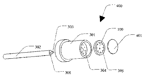
FIG. 4 is a probe assembly drawing. The exemplary probe 400 comprises a
microstrip patch antenna 100 placed inside of a probe body 301. A microwave
cable 302 is
placed through the back side of the probe body 301 and attached to the antenna
100. A
dielectric window 401 is placed over microstrip patch antenna 100 in order to
provide a
thermal and environmental barrier .that increases the life of probe 400 within
a high
temperature environment.
Probe 400 is identical to the probe 300 of FIG. 3 with the addition of the
dielectric
window placed over the top of microstrip patch antenna 100. The dielectric
window 401 can
be thin, on the order of several thousandths of an inch thick. Windows are
typically applied
using a plasma flame spray, with standard materials such as yittria-stabilized
zirconia (YTZ).
The flame spray provides an environmental barrier over metallization 101 that
keeps oxygen
8
CA 02597621 2007-08-10
WO 2006/086611 PCT/US2006/004697
from reaching the metal. This significantly reduces the oxidation rate of
metallization 101
and extends the overall life within the high temperature application. In
exemplary
applications, the thickness of the dielectric window 401, when applied using a
flame spray
coating, is typically small enough to avoid having a significant effect on the
microwave
performance of patch antenna 100. Therefore, patch antenna 100 can normally be
designed
using standard antenna design techniques and the flame spray dielectric window
401 can be
applied to patch antenna 100 at the end of the process without any appreciable
change in
antenna performance.
The dielectric window 401 also can be implemented as a thick disk of material
placed
over patch antenna 100. The window material can include alumina, silicon
dioxide, or any
other material deemed appropriate for the application, with a thickness of up
to or exceeding
one half an inch thick. When a large dielectric window is placed in front of
patch antenna
100, the microwave performance of the antenna can be impacted. Therefore, when
a thick
dielectric window 401 is used, the microwave design will have to properly
account for its
presence by impedance matching the patch to the dielectric window.
A large dielectric window 401 is typically attached using a ceramic adhesive
to bond
the dielectric substrate 102. Other standard metal to ceramic techniques can
be used to attach
the dielectric window 401 to the high temperature metallization 101.
FIG. 5 shows a cross-section of a fully assembled probe without cooling holes
in
probe body 301. The cable 302 is inserted through a hole in the back of probe
body 301 and
attached to patch antenna 100. The probe body 301 provides the electrical
ground connection
between cable 302 and patch antenna 100. The entire assembly is preferably
assembled in a
manner that allows all of the metal pieces to have strong electrical grounds.
Without a
sufficient metal-to-metal contact, the antenna center frequency and notch
depth can be
adversely affected and antenna performance will be sub-optimal.
FIG. 6 shows a cross section of a fully assembled probe containing cooling
holes 304
in probe body 301. For this embodiment, probe body 301 includes outer walls of
a sufficient
thickness to allow cooling holes 304 to be machined. Probe body 301 is
typically installed in
such a way that the cooling holes furthest away from patch antenna 100 are
located in an area
of relatively cool air while the holes through and above the patch antenna 100
are located
within the high temperature environment. In a typical installation, such as a
gas turbine
engine, the cooler air passes through the probe body into the high temperature
area. Along
the way, the cooler air takes heat out of probe body 301, cable 302, and patch
antenna 100.
In exemplary designs within turbine engines, temperatures can be reduced by
several hundred
9
CA 02597621 2007-08-10
WO 2006/086611 PCT/US2006/004697
degrees Fahrenheit by the addition of the cooling holes in the probe body,
which can
significantly improve probe life. The cooling holes 304 shown in this
exemplary design can
be of any geometry that is compatible with the installation and environment
and sufficient to
support cooling flow to enable long life operation.
FIG. 7 shows a cross section of an exemplary probe assembly with areas of high
temperature joining necessary in the probe assembly process. Joint 701 is
typically a laser
weld or TIG weld that attaches cable 302 with probe body 301. It is normally
desirable to
have joint 701 to be hermetic so that contamination of cable 302 is minimized.
Joint 702 is a ceramic to metal seal that attaches probe body 301 to the
dielectric
substrate 102. In exemplary designs, a vacuum brazed is used. However, air
brazing, torch
brazing, and diffusion bonding are additional ways to create the seal. Any
conventional
ceramic-to-metal seal methodology may be used to create the seal provided that
the seal can
handle the thermal and chemical environments where it is operating and provide
the required
hermetic seal for the cable.
Joint 704 attaches the center conductor of the cable 303 to the high
temperature
metallization 101 or disk 201. The attachment must provide sufficient
electrical contact as to
allow the microwave energy to transition from the cable to the patch antenna
100 with
minimal signal reflections or losses. In exemplary implementations, a laser
weld is used for
the attachment. Brazing, TIG welding, induction heating, and any other metal
to metal
attachment process can be used without loss of generality.
FIG. 8 shows a typical probe installation inside of a gas turbine engine. The
assembled probe comprises probe body 301, cable 302, and patch antenna 100 and
supports a
measurement of the distance to the turbine blade 901 rotating by the probe.
The probe is
mounted into the side of the turbine case 902 using a boss or other insert 903
which matches
the dimensions of the hole in case 902 with the outer geometry of probe body
301. In the
hottest areas of the engine, the. gas going past turbine blade 901 can exceed
2000 F. This
installation also shows the cooling holes in probe body 301 in this case,
implemented as an
annulus 904. By using an annulus instead of discrete cooling holes, a larger
amount of air
flow can be forced through the probe.
In view of the foregoing, it will be understood that the present invention
comprises an
antenna operational within a high temperature environment. An antenna
radiating element,
typically comprising a patch formed by a conductive element in contact with a
dielectric
element, is operative to communicate electromagnetic signals. The dielectric
element of the
antenna radiating element typically comprises a dielectric material exhibiting
a low change in
CA 02597621 2007-08-10
WO 2006/086611 PCT/US2006/004697
dielectric constant as a function of temperature. A housing comprising
conductive material is
operable to accept the antenna radiating element. This housing has one or more
cooling
orifices supporting the passage of air for cooling the antenna radiating
element within the
high temperature environment.
A high temperature microwave cable can be coupled to the antenna radiating
element.
The cable is typically inserted within the housing and attached to the
conductive element of
the antenna radiating element for the passage of electromagnetic signals to or
from the
radiating element.
A dielectric window can be positioned in front of the antenna radiating
element and
adjacent to the housing. The dielectric window comprising a dielectric
material operative to
provide additional thermal and environmental protection for the antenna
radiating element.
The dielectric window typically comprises a flame spray coating or a
dielectric material.
The antenna radiating element is typically housed within at least a portion of
the
housing and joined to the housing by a bond capable of withstanding the high
temperature
environment. The housing can comprise a conductive material having dimensions
sufficient
to operate as a ground plane for the antenna radiating element.
The conductive element can comprise a metallization applied to a surface of
the
dielectric element. In the alternative, the conductive element can comprises a
solid
conductive material joined to a surface of the dielectric element. The
conductive element
typically has a geometry suitable for communication of electromagnetic
signals.
The dielectric element can comprises one or more orifices or cooling holes to
support
the passage of air for cooling the antenna within the high temperature
environment.' In the
alternative, the dielectric element can comprise an annular passage to
.support the passage of
air for cooling the antenna within the high temperature' environment. , The
antenna also can
include one or more passages positioned adjacent to the dielectric element to
support the
passage of air for cooling the antenna within the high temperature
environment.
The present invention also provides a method of manufacturing an antenna for
operation within a high temperature environment. An antenna radiating element
can be
formed by joining a conductive element to a dielectric material element. At
least one orifice
is added to a housing for housing the antenna radiating element. Orifices can
be added to the
conductive element of the antenna radiating element to further support the
distribution 'of air
for cooling the antenna. Each orifice or cooling hole supports the passage of
air from the
exterior of the housing to the interior of the housing for cooling the antenna
within the high
11
CA 02597621 2007-08-10
WO 2006/086611 PCT/US2006/004697
temperature environment. The antenna radiating element is inserted within at
least a portion
of the housing and joined to the housing.
The present application has presented alternative exemplary embodiments of a
patch
antenna operable within a high temperature environment. Different applications
will require
different frequencies of operation, mechanical dimensions and geometries, and
materials,
which can be designed using techniques known to one versed in the art.
12