Note: Descriptions are shown in the official language in which they were submitted.
CA 02598740 2007-08-23
WO 2006/091791 PCT/US2006/006552
METHODS AND APPARATUS FOR ACTUATING DISPLAYS
Field of the Invention
In general, the invention relates to the field of video displays, in
particular,
the invention relates to mechanically actuated display apparatus.
Background of the Invention
Displays built from mechanical light modtilators are an attractive alternative
to displays based on liquid crystal technology. Mechanical light modulators
are fast
enough to display video content with good viewing angles and with a wide range
of
color and grey scale. Mechanical light modulators have been successful in
projection display applications. Baclclit displays using mechanical light
modulators
have not yet demonstrated sufficiently attractive combinations of brightness
and low
power. There is a need in the art for fast, bright, low-powered mechanically
actuated displays. Specifically there is a need for mechanically acttiated
displays that
include bi-stable mechanisms and that can be driven at low voltages for
reduced
power consumption.
Suinmary of the Invention
In one aspect, the invention relates to displays built from mechanical
actuators which incorporate two compliant electrodes. The actuators may be
controlled by passive or active matrix arrays coupling controllable voltage
sources to
the voltage inputs of the mechanical actuators.
The compliant electrodes in each actuator are positioned proximate to one
another, such that in response to the application of a voltage across the
electrodes,
the electrodes are drawn togetlier. The electrodes may be drawn together
directly or
progressively. At least one of the electrodes couples to a modulator which
contributes to the formation of an image. According to one feature of the
invention,
at least a majority of the lengths of the electrodes are compliant. The
electrodes may
be about 0.5 m to about 5 gm wide. In one implementation, the height of the
electrodes is at least about 1.4 times the width of the electrodes. The
electrodes may
also be coated, at least in part with an insulator, preferably having a
dielectric
constant of about 1.5 or greater.
CA 02598740 2007-08-23
WO 2006/091791 PCT/US2006/006552
The modulator may be, for example, a shutter, a deformable mirror, a color
filter, or a set of three color filters. Sliutters move substantially in a
plane parallel to
a surface over which they are supported. The surface may have one or more
apertures allowing the passage of light through the surface. The apertures may
be
patterned through a reflective film disposed on a substantially transparent
glass or
plastic substrate. If the surface has more than one aperture, the shutter
includes a
corresponding number of shutter apertures. By moving the sllutter, the display
apparatus can selectively interact with light in an optical path passing
through the
apertures in the surface by either blocking, reflecting, absorbing,
polarizing,
diffracting and/or filtering the light. In various embodiments, the shutter
may also
be coated with a reflective or light absorbing film.
In one embodiment, one end of each electrode is anchored to the surface and
the other end is free to move. In this embodiment, the modulator couples to
the free
end of one of the electrodes. The width of the electrode may be constant along
its
length, or it may vary. For example, it may become tliinner closer to the
modulator.
Alternatively, the electrode may have thinner sections and thicker sections at
multiple locations along the length of the electrode. The varying thicknesses
provide for varying electrode stiffnesses. The embodiment may include an
optional
feature of including a third compliant electrode. The compliant electrodes not
coupled to the modulator act separately as open and close drive electrodes.
One or
both of the drive electrodes may be curved in its natural, deactivated state.
In some
implementations, the drive electrodes have a first or second order curve. In
other
implementations, the drive electrodes have a greater than second order curve.
In another embodiment of the shutter assembly, a shutter couples to a pair of
actuators at about the linear center of one side of the modulator. The
actuators each
include two compliant electrodes. A first compliant electrode of each actuator
couples to the shutter with a spring. The first compliant electrode may also
couple
to the anchor with a spring. The other ends of the compliant electrodes couple
to
anchors, thereby coiuiecting the shutter to two locations on a substrate. The
electrodes serve as mechanical supports providing supportive connections from
locations on the shutter to the substrate. A separate elastic member, such as
a return
spring, may couple to an opposite side of the shutter, providing an additional
-2-
CA 02598740 2007-08-23
WO 2006/091791 PCT/US2006/006552
supportive connection for the shutter. Alternatively, a second pair of
actuators may
couple to the opposite side of the shutter instead of the return spring. The
multiple
supportive connections help reduce rotation or other movement of the shutter
out of
its intended plane of motion.
In a second aspect of the invention, the display apparatus includes a
mechanically bi-stable sliutter assembly to form an image. A mechanically bi-
stable
shutter assembly includes a shutter, a voltage input for receiving an
actuation
potential and an actuator that moves a shutter over a substrate between two
mechanically stable positions. In one embodiment, the work needed to move the
shutter from its first mechanically stable position to its second mechanically
stable
position is greater than the worlc need to return the shutter to its first
mechanically
stable position. In another einbodiment, the amount of worlc needed to move
the
shutter from its first mechanically stable position to its second mechanically
stable
position is substantially equal to the work needed to retuni the shutter to
its first
mechanically stable position.
According to one feature of the invention, the mechanically stable positions
of the sllutter are provided by the state, including the position or shape, of
a
mechanically compliant member. In one embodiment, the mechanically compliant
member is part of the actuator. In other embodiments, the mechanically
compliant
meinber is outside of the actuator. The mechanically compliant member has a
first
mechanically stable state in a first of the shutter's mechanically stable
positions and
a second mechanically stable state in the second of the shutter's mechanically
stable
position. Moving the shutter from the first mechanically stable position to
the
second mechanically stable position requires the defonnation of the compliant
member.
For example, the compliant member may be a curved compliant beam.
When the shutter is in the first stable position, the beam has a first
curvature. The
beam has a second curvature when the shutter is in the second position. The
curvature may be generally "s" shaped or it may form a cosine shaped bow. In
the
first shutter position, the beam may bow in one direction. In transitioning to
the
-3-
CA 02598740 2007-08-23
WO 2006/091791 PCT/US2006/006552
second shutter position, the beam is deformed such that bows in an opposite
direction.
Alternatively, the compliant beam may be straight while the shutter is in one
of its mechanically stable position. The compliant beam forms a first angle
with the
shutter in the first mechanically stable shutter position. In the second
position, the
compliant beam forms a different angle wit11 the shutter.
The shutter assembly may also include a second compliant member. The
first and second compliant members, in one embodiment, serve as electrodes in
a
dual compliant beain electrode actuator. One or both beams may have two
mechanically stable states. Upon application of a voltage across the compliant
members, one of the coinpliant members deforms from one position to a second
position. The voltage may result from an actuation potential being applied to
one of
the compliant members from one or more anchors coupled to one or both ends of
the
compliant member. For example, in the first position, the first compliant
electrode
bows away from the second coinpliant electrode. In the second position, the
first
compliant electrode bows towards the second compliant electrode, having a
substantially similar bow as the second compliant electrode. In other
implementations, the first and second compliant beams fonn part of a
thermoelectric
actuator coupled to the shutter for moving it between the first and second
stable
positions. Regardless of the type of actuator moving the shutter, to move the
shutter, a force must be applied to either the first or second compliant
member.
Iii some embodiments, the first and second compliant member shapes are
themselves mechanically stable.
The shutter assembly, in one implementation, includes a second actuator
coupled to the shutter. The two actuators couple to the shutter in different
locations
on the shutter. According to one implementation, the actuators couple to
opposite
sides of the shutter, at about the middle of the sides. Compliant members in
the
actuators provide supportive connections for the shutter from two shutter
locations
to two substrate locations. According to another optional feature, at least
one of the
compliant members coupled to the shutter couples to two anchors, one on either
end
the compliant member.
-4-
CA 02598740 2007-08-23
WO 2006/091791 PCT/US2006/006552
In still other embodiments, the compliant members are incorporated into a
stabilizer which provides the mechanical stability for the mechanically stable
shutter
positions. The compliant members in a stabilizer may be connected to one
another.
In such an embodiment, the stabilizer may provide for a third mechanically
stable
shutter position. The shutter is driven into the tliird mechanically stable
shutter
position in response to an application of a second actuation voltage to the
voltage
input. Alternatively, the compliant beams may form a stabilizer by coupling to
anchors on either side of the shutter to sides of the shutter. The compliant
members
may include compliant or rigid beams. If the compliant members include rigid
beams, the compliant members include additional coinpliant joints between the
rigid
beams to provide a degree of compliance.
Additional features of the various display apparatus include the incorporation
of a working fluid among the compliant members. The worlcing fluid preferably
has
a dielectric constant of at least about 1.5. The display apparatus may also
include a
baclcliglit for illuminating the image.
In anotlier aspect, the invention relates to a method of manufacturing a
display apparatus. The method includes patterning a first surface to form a
modulator for selectively interacting with light in an optical path. An
actuator is
then fabricated in the first surface comiecting the modulator and an anchor.
The
anchor and the actuator serve as a first mechanical support, physically
supporting the
modulator over a second surface. The actuator is configured to drive the
shutter in a
plane substantially parallel to the second surface. The method further
includes
fabricating a second mechanical support into first surface connecting the
modulator
and a second anchor. The second mechanical support physically supports the
modulator over the second surface. The first anchor and the second anchor are
connected to two distinct locations on the second surface.
In another aspect, the invention relates to a method of forming an image.
The method includes selectively applying an actuation potential to a voltage
input of
a shutter assembly. A shutter is moved in a plane substantially parallel to a
surface,
in response to the application of the actuation voltage. The sllutter is moved
from a
-5-
CA 02598740 2007-08-23
WO 2006/091791 PCT/US2006/006552
first mechanically stable position to a second mechanically stable position,
thereby
permitting light to contribute to the formation of an image.
In still a further aspect, the invention relates to a method of forming an
image
on a display. The method includes selecting a light modulator and providing an
actuator. The actuator includes two mechanically compliant electrodes
positioned
proximate to one another, at least one of which couples to a shutter. The
actuator is
activated by generating a voltage between the two mechanically compliant
electrodes. As a result, the compliant electrodes deform as they are drawn
closer
together. In addition, the activation of the actuator results in movement of
the
shutter into or out of an optical path to affect the illumination of a pixel
in the image.
Brief Description of the Drawings
The system and methods may be better understood from the following
illustrative description with reference to the following drawings in which:
Figure 1 is conceptual isometric view of a display apparatus, according to an
illustrative embodiment of the invention;
Figures 2A-2B are top views of dual compliant beam electrode actuator-
based shutter assemblies for use in a display apparatus, according to an
illustrative
embodiment of the invention;
Figure 3A is a diagram illustrating various compliant electrode shapes
suitable for inclusion in dual compliant electrode actuator-based shutter
assemblies;
Figure 3B is a diagram illustrating the incremental energy needed to move
dual compliant electrode actuator-based shutter assemblies having the shapes
illustrated in Figure 3A;
Figures 3C-3F are top views of the compliant beam electrode actuator-based
shutter assembly of Figure 2A in various stages of actuation.
Figures 4A and 4B are cross section views of a dual compliant electrode
actuator-based mirror-based light modulator in an active and an inactive
state,
according to an illustrative embodiment of the invention;
-6-
CA 02598740 2007-08-23
WO 2006/091791 PCT/US2006/006552
Figure 5 is a top view of a dual compliant beam electrode actuator-based
shutter assembly having a beam with thiclcness which varies along its length,
according to an illustrative embodiment of the invention;
Figure 6 is an isometric view of a dual compliant beam electrode actuator-
based shutter assembly, according to an illustrative embodiment of the
invention;
Figure 7 is a top view of a dual compliant beam electrode actuator-based
shutter assembly including a return spring, according to an illustrative
einbodiment
of the invention;
Figure 8 is a top view of a dual compliant beam electrode actuator-based
shutter assembly having separate open and close actuators, according to an
illustrative embodiment of the invention;
Figure 9 is a conceptual diagram of an active matrix array for controlling
dual compliant electrode actuator based-light modulators, according to an
illustrative
embodiment of the invention;
Figure 10 is a conceptual diagram of a second active matrix array for
controlling dual compliant electrode actuator based-light modulators,
according to
an illustrative embodiment of the invention;
Figure 11 is a cross sectional view of the dual compliant beam electrode
actuator-based shutter assembly of Figure 8;
Figure 12 is an energy diagram illustrating the energy characteristics of
various dual compliant electrode based shutter assemblies, according to an
illustrative embodiment of the invention;
Figure 13A is a top view of a bi-stable dual compliant beain electrode
actuator based-shutter assembly, according to an illustrative embodiment of
the
invention;
Figure 13B shows the evolution of force versus displacement for a bi-stable
shutter assembly.
-7-
CA 02598740 2007-08-23
WO 2006/091791 PCT/US2006/006552
Figure 14 is a top view of a second bi-stable dual compliant beam electrode
actuator based-shutter assembly, according to an illustrative embodiment of
the
invention;
Figure 15 is a top view of a tri-stable shutter assembly incorporating dual
compliant electrode actuators, according to an illustrative embodiment of the
invention;
Figures 16A C are conceptual diagrams of another embodiment of a bi-
stable shutter assembly, illustrating the state of the shutter assembly during
a change
in shutter position, according to an illustrative embodiment of the invention;
Figure 17A is a conceptual diagram of a bi-stable shutter assembly including
substantially rigid beams, according to an illustrative embodiment of the
invention;
Figure 17B is a top view of a rotational bi-stable shutter assembly;
Figure 18 is a conceptual diagram of a bi-stable shutter assembly
incorporating thermoelectric actuators, according to an illustrative
embodiment of
the invention;
Figure 19 is a conceptual diagram of a passive matrix array for controlling
bi-stable shutter assemblies, according to an illustrative embodiinent of the
invention;
Figures 20A and 20B are conceptual tiling diagrams for arranging sl7utter
assemblies in a display apparatus; and
Figure 21 is cross-sectional view of a display apparatus, according to an
illustrative embodiment of the invention.
Figure 22 is cross-sectional view of another display apparatus, according to
an illustrative embodiment of the invention.
Description of Certain Illustrative Embodiments
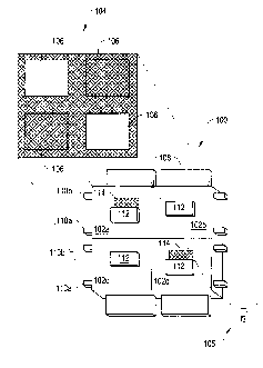
Figure 1A is an isometric view of a display apparatus 100, according to an
illustrative embodiment of the invention. The display apparatus 100 includes a
plurality of light modulators, in particular, a plurality of shutter
assemblies 102a-
102d (generally "shutter assemblies 102") arranged in rows and colunms. In
-8-
CA 02598740 2007-08-23
WO 2006/091791 PCT/US2006/006552
general, a shutter assembly 102 has two states, open and closed (although
partial
openings can be employed to impart grey scale). Sliutter assemblies 102a and
102d
are in the open state, allowing light to pass. Shutter assemblies 102b and
102c are in
the closed state, obstructing the passage of light. By selectively setting the
states of
the shutter assemblies 102a-102d, the display apparatus 100 can be utilized to
fonn
an image 104 for a projection or backlit display, if illuminated by lamp 105.
In
another implementation the apparatus 100 may form an image by reflection of
ambient light originating from the front of the apparatus. In the display
apparatus
100, each shutter assembly 102 corresponds to a pixel 106 in the image 104.
Each shutter asseinbly 102 includes a shutter 112 and an aperture 114. To
illuminate a pixel 106 in the image 104, the shutter 112 is positioned such
that it
allows light to pass, without any significant obstruction, through, the
aperture 114
towards a viewer. To keep a pixel 106 unlit, the shutter 112 is positioned
such that
it obstructs the passage of light through the aperture 114. The aperture 114
is
defined by an opening patterned through a reflective or light-absorbing
material in
each shutter assembly 102.
In alternative impleinentations, a display apparatus 100 includes multiple
shutter assemblies 102 for each pixel 106. For example, the display apparatus
100
may include three color-specific shutter assemblies 102. By selectively
opening one
or more of the color-specific shutter assemblies 102 corresponding to a
particular
pixel 106, the display apparatus 100 can generate a color pixel 106 in the
image 104.
In another example, the display apparatus 100 includes two or more shutter
assemblies 102 per pixel 106 to provide grayscale in an image 104. In still
other
implementations, the display apparatus 100 may include other forms of light
modulators, such as micromirrors, filters, polarizers, interferometric
devices, and
other suitable devices, instead of shutter assemblies 102 to modulate light to
form an
image.
The shutter assemblies 102 of the display apparatus 100 are fonned using
standard micromachining techniques known in the art, including lithograpliy;
etching techniques, such as wet chemical, dry, and photoresist removal;
thermal
oxidation of silicon; electroplating and electroless plating; diffusion
processes, such
as boron, phosphorus, arsenic, and antimony diffusion; ion implantation; film
-9-
CA 02598740 2007-08-23
WO 2006/091791 PCT/US2006/006552
deposition, such as evaporation (filament, electron beam, flash, and shadowing
and
step coverage), sputtering, chemical vapor deposition (CVD), plasma enhanced
CVD, epitaxy (vapor phase, liquid phase, and molecular beam), electroplating,
screen printing, and lamination. See generally Jaeger, Introduction to
Microelectronic Fabrication (Addison-Wesley Publishing Co., Reading Mass.
1988); Runyan, et al., Semiconductor Integrated Circuit Processing Technology
(Addison-Wesley Publishing Co., Reading Mass. 1990); Proceedings of the IEEE
Micro Electro Mechanical Systems Conference 1987-1998; Rai-Choudhury, ed.,
Handbook of Microlitllography, Micromachining & Microfabrication (SPIE Optical
Engineering Press, Bellinghain, Wash. 1997).
More specifically, multiple layers of material (typically alternating between
metals and dielectrics) are deposited on top of a substrate forming a stack.
After one
or more layers of material are added to the stack, patterns are applied to a
top most
layer of the stack marlcing material eitlier to be removed from, or to remain
on, the
stack. Various etching techniques, including wet or dry etches or reactive ion
etching, are then applied to the patterned stack to remove unwanted material.
The
etch process may remove material from one or more layers of the stack based on
the
chemistry of the etch, the layers in the stack, and the amount of time the
etch is
applied. The manufacturing process may include multiple iterations of
layering,
patterning, and etching.
In one implementation the shutter asseinblies 102 are fabricated upon a
transparent glass or plastic substrate. This substrate may be made an integral
part of
a backlight which acts to evenly distribute the illumination from lamp 105
before the
light exits through apertures 114. Alternatively and optionally the
transparent
substrate may be placed on top of a planar light guide, wherein the array of
shutter
assemblies 102 act as light modulation elements in the formation of an image.
In one
implementation the shutter assemblies 102 are fabricated in conjunction with
or
subsequent to the fabrication of a thin film transistor (TFT) array on the
same glass
or plastic substrate. The TFT array provides a switching matrix for
distribution of
electrical signals to the shutter assemblies.
-10-
CA 02598740 2007-08-23
WO 2006/091791 PCT/US2006/006552
The process also includes a release step. To provide freedom for parts to
move in the resulting device, sacrificial material is interdisposed in the
stack
proximate to material that will form moving parts in the completed device. An
etch
removes much of the sacrificial material, thereby freeing the parts to move.
After release, one or more of the surfaces of the shutter assembly may be
insulated so that charge does not transfer between moving parts upon contact.
This
can be accomplished by thermal oxidation and/or by conformal chemical vapor
deposition of an insulator such as A1203, Cr203, Ti02, TiSiO4, Hf02, HfSiO4,
V205, Nb205, Ta205, Si02, or Si3N4 or by depositing similar materials using
techniques such as atomic layer deposition and others. The insulated surfaces
are
chemically passivated to prevent problems suclz as stiction between surfaces
in
contact by chemical conversion processes such as fluoridation, silanization,
or
hydrogenation of the insulated surfaces.
Dual compliant electrode actuators make up one suitable class of actuators
for driving the shutters 112 in the shutter assemblies 102. A dual compliant
beam
electrode actuator, in general, is formed from two or more at least partially
compliant beams. At least two of the beams serve as electrodes ( also referred
to
herein as "beam electrodes"). In response to applying a voltage across the
beam
electrodes, the beams electrodes are attracted to one another from the
resultant
electrostatic forces. Both beams in a dual compliant beam electrode are, at
least in
part, compliant. That is, at least some portion of each of the beams can flex
and or
bend to aid in the beams being brought together. In some iinpleinentations the
compliance is achieved by the inclusion of flexures or pin joints. Some
portion of
the beams may be substantially rigid or fixed in place. Preferably, at least
the
majority of the length of the beams are compliant.
Dual compliant electrode actuators have advantages over other actuators
known in the art. Electrostatic comb drives are well suited for actuating over
relatively long distances, but can generate only relatively weak forces.
Parallel plate
or parallel beam actuators can generate relatively large forces but require
small gaps
between the parallel plates or beams and therefore only actuate over
relatively small
distances. R. Legtenberg et. al. (Journal of Microelectromechanical Systems
v.6, p.
257, 1997) demonstrated how the use of curved electrode actuators can generate
-11-
CA 02598740 2007-08-23
WO 2006/091791 PCT/US2006/006552
relatively large forces and result in relatively large displacements. The
voltages
required to initiate actuation in Legtenberg, however, are still substantial.
As shown
herein such voltages can be reduced by allowing for the movement or flexure of
both electrodes.
In a dual compliant beam electrode actuator-based shutter assembly, a shutter
is coupled to at least one beain of a dual coinpliant beam electrode actuator.
As one
of the beatns in the actuator is pulled towards the other, the pulled beam
moves the
shutter, too. In doing so, the shutter is moved from a first position to a
second
position. In one of the positions, the shutter interacts with light in an
optical path
by, for example, and without limitation, blocking, reflecting, absorbing,
filtering,
polarizing, diffracting, or otherwise altering a property or patll of the
light. The
shutter may be coated with a reflective or light absorbing film to improve its
interferential properties. In the second position, the shutter allows the
light to pass
by, relatively unobstructed.
Figures 2A and 2B are diagrams of two embodiments of cantilever dual
compliant beam electrode actuator based-shutter asseinblies for use in a
display
apparatus, such as display apparatus 100. More particularly, Figure 2A depicts
a
cantilever dual compliant beam electrode actuator-based shutter assembly 200a
("shutter assembly 200a"). The shutter assembly 200a modulates light to form
an
image by controllably moving a shutter 202a in and out of an optical path of
light.
In one embodiment, the optical path begins behind a surface 204a, to which the
shutter 202a is attached. The surface 204a is illustrated as dashed boundary
line.
The dashed line indicates that the surface 204a extends beyond the space
delimited
by the boundary line. Similar dashed boundary lines are used in other figures
to
indicate the same. The light passes through an aperture 206a in the surface
204a
towards a viewer or towards a display screen. In another embodiment, the
optical
path begins in front of the surface 204a and is reflected back to the viewer
from the
surface of the aperture 206a.
The shutter 202a of the shutter assembly 200a is formed from a solid,
substantially planar, body. The shutter 202a can take virtually any shape,
either
regular or irregular, such that in a closed position the shutter 202a
sufficiently
obstructs the optical path through the aperture 206a in the surface 204a. In
addition,
-12-
CA 02598740 2007-08-23
WO 2006/091791 PCT/US2006/006552
the shutter 202a must have a width consistent with the width of the aperture,
that, in
the open position (as depicted), sufficient light can pass through the
aperture 206a in
the surface 204a to illuminate a pixel, or contribute to the illumination of a
pixel, in
the display apparatus.
The shutter 202a couples to one end of a load beam 208a. A load anchor
210a, at the opposite end of the load beam 208a physically connects the load
beam
208a to the surface 204a and electrically connects the load beam 208a to
driver
circuitry in the surface 204a. Together, the load 208a beam and load anchor
210a
serve as a mechanical support for supporting the shutter 202a over the surface
204a.
The shutter assembly 200a includes a pair of drive beams 212a and 214a, one
located along either side of the load beam 210a. Together, the drive beams
212a and
214a and the load beam 210a form an actuator. One drive beam 212a serves as a
shutter open electrode and the other drive beam 214a serves as a shutter close
electrode. Drive anchors 216a and 218a located at the ends of the drive beams
212a
and 214a closest to the shutter 202a physically and electrically connects each
drive
beam 212a and 214a to the surface 204a. In this embodiment, the other ends and
most of the lengths of the drive beams 212a and 214a remain unanchored or
free.
The free ends of the drive beams 212a and 214a are closer to the anchored end
of the
load beam 208a than the anchored ends of the drive beams 212a and 214a are to
shutter end of the load beam208a.
The load beam 208a and the drive beams 212a and 214a are compliant. That
is, they have sufficient flexibility and resiliency that they can be bent out
of their
unstressed ("rest") position or shape to at least some useful degree, without
fatigue
or fracture. As the load beain 208a and the drive beams 212a and 214a are
anchored
only at one end, the majority of the lengths of the beams 208a, 212a, and 214a
is
free to move, bend, flex, or deform in response to an applied force. The
operation of
the cantilever dual compliant beam electrode actuator based-shutter assembly
200a
is discussed further below in relation to Figure 3.
Figure 2B is a second illustrative embodiment of a cantilever dual compliant
beain electrode actuator-based shutter assembly 200b (shutter assembly 200b).
Like
the shutter assembly 200a, the shutter assembly 200b includes a shutter 202b,
coupled to a load beam 208b, and two drive beams 212b and 214b. The shutter
-13-
CA 02598740 2007-08-23
WO 2006/091791 PCT/US2006/006552
202b is positioned in between its fully open position and its fully closed
position.
The load beam 208b and the drive beams 212b and 214b, together, form an
actuator.
Drive anchors 210b, 216b and 218b, coupled to each end of the beams connect
the
beams to a surface 204b. In contrast to the shutter assembly 200a, the shutter
of
shutter assembly 200b includes several shutter apertures 220, in the form of
slots.
The surface 204b, instead of only having one aperture, includes one surface
aperture
206b corresponding to each shutter aperture 220. In the open position, the
shutter
apertures 220 substantially align with the apertures 206b in the surface 204b,
allowing light to pass through the shutter 202b. In the closed position, the
surface
apertures 206b are obstructed by the remainder of the shutter 202b, thereby
preventing the passage of light.
Changing the state of a shutter assembly that includes multiple shutter
apertures with a corresponding number of surface apertures requires less
shutter
movement than changing the state of a shutter assembly incorporating a solid
shutter
and single surface aperture, while still providing for the same aperture area.
Reduced required motion corresponds to lower required actuation voltage. More
particularly, a decrease in required motion by 1/3 reduces the necessary
actuation
voltage of the actuator by a factor of about 1/3. Reduced actuation voltage
further
corresponds to reduced power consumption. Since the total aperture area for
either
shutter assembly is about the same, each shutter assembly provides a
substantially
similar brightness.
In other implementations, the shutter apertures and corresponding surface
apertures have shapes other than slots. The apertures may be circular,
polygonal or
irregular. In alternative implementations, the shutter may include more
shutter
apertures than there are surface apertures in the shutter assembly. In such
implementations, one or more of the shutter apertures may be serve as a
filter, such
as color filter. For example, the shutter assembly may have three shutter
apertures
for every surface aperture, each shutter aperture including a red, blue, or
green
colored filter.
Figures 3A and 3B are diagrams illustrating the relationship between the,
displacement at the end of the load beam and the relative voltage needed to
move the
load beam closer to the drive beam. The displacement that can be achieved at
any
-14-
CA 02598740 2007-08-23
WO 2006/091791 PCT/US2006/006552
given voltage depends, at least in part, on the curvature or shape of the
drive beam,
or more precisely, on how the separation, d, and the bending stress along the
drive
beam and the load beam varies as a function of position x along the load beam
A
separation function d(x), shown in Figure 3A can be generalized to the form of
d=ax", where y is the distance between the beams. For example, if n =1, the
distance
between drive electrode and load electrode increase linearly along the length
of the
load electrode. If n=2, the distance increases parabolically. In general,
assuming a
constant voltage, as the distance between the compliant electrodes decreases,
the
electrostatic force at any point on the beams increases proportional to 1/d.
At the
same time, however, any deformation of the load beam which might decrease the
separation distance may also results in a higher stress state in the beam.
Below a
minimum threshold voltage a limit of defonnation will be reached at which any
electrical energy released by a closer approach of the electrodes is exactly
balanced
by the energy which becomes stored in the deformation energy of the beams.
As indicated in the diagram 3B, for actuators having separation fiuictions in
which n is less than or equal to 2, the application of a minimum actuation
voltage
(V2) results in a cascading attraction of the load beam to the drive beam
without
requiring the application of a higher voltage. For such actuators, the
incremental
increase in electrostatic force on the beams resulting from the load beam
getting
closer to the drive beam is greater than the incremental increase in stress on
the
beams needed for further displacement of the beams.
For actuators having separation functions in which x is greater than 2, the
application of a particular voltage results in a distinct partial displacement
of the
load electrode. That is, the incremental increase in electrostatic force on
the beams
resulting from a particular decrease in separation between the beams, at some
point,
fails to exceed the incremental deformation force needed to be imparted on the
load
beam to continue reducing the separation. Thus, for actuators having
separation
functions having n greater than 2, the application of a first voltage level
results in a
first corresponding displacement of the load electrode. A higher voltage
results in a
greater corresponding displacement of the load electrode. How the shapes and
relative compliance of thin beam electrodes effects actuation voltage is
discussed in
more detail in the following references: (R. Legtenberg et. al., Journal of
-15-
CA 02598740 2007-08-23
WO 2006/091791 PCT/US2006/006552
Microelectromechanical Systems v.6, p. 257 (1997) and J. Li et. al.
Transducers '03,
The 12t" International Conference on Solid State Sensors, Actuators, and
Microsystems, p. 480 (2003).
Referring back to Figures 2A and 2B, a display apparatus incorporating the
shutter assemblies 202a and 202b actuates, i.e., changes the position of the
shutter
assemblies 202a and 202b, by applying an electric potential, from a
controllable
voltage source, to one of the drive beams 212a, 212b, 214a, or 214b via its
corresponding drive anchor 216a, 216b, 218a, or 218b, with the load beam 208a
or
208b being electrically coupled to ground, resulting in a voltage across the
beams208a, 208b, 212a, 212b, 214a, 214b. The controllable voltage source, such
as
an active matrix array driver, is electrically coupled to load beam 208a or
208b via
an active matrix array (see Figures 9 and 10 below). The display apparatus may
instead apply a potential to the load beam 208a or 208b via the load anchor
210a or
210b of the shutter assembly 202a or 202b to increase the voltage. An
electrical
potential difference between the drive beams and the load beams, regardless of
sign
or ground potential, will generate an electrostatic force between the beams.
With reference back to Figure 3, the shutter assembly 200a of Figure 2A has
a second order separation function (i.e., n=2). Thus, if the voltage or
potential
difference between the beams 208a and 212a or 214a of the shutter assembly
202a
at their point of least separation exceeds the minimum actuation voltage (V2)
the
deformation of the beams 208a and 212a or 214a cascades down the entire
lengtlls
of the beams 208a and 212a or 214a, pulling the shutter end of the load beam
208a
towards the anchored end of the drive beani 212a or 214a. The motion of the
load
beam 208a displaces the shutter 202a such that it changes its position from
either
open to closed, or visa versa, depending on to which drive beam 212a or 214a
the
display apparatus applied the potential. To reverse the position change, the
display
apparatus ceases application of the potential to the energized drive beam 212a
or
214a. Upon the display apparatus ceasing to apply the potential, energy stored
in the
form of stress on the defonned load beam 208a restores the load beam 208a to
its
original or rest position. To increase the speed of the restoration and to
reduce any
oscillation about the rest position of the load beam 208a, the display
apparatus may
-16-
CA 02598740 2007-08-23
WO 2006/091791 PCT/US2006/006552
return the shutter 202a to its prior position by applying an electric
potential to the
opposing drive beam 212a or 214a.
This shutter assemblies 200a and 200b, as well as shutter assemblies 500
(see Figure 5 below), 600 (see Figure 6 below), 700 (see Figure 7 below) and
800
(see Figure 8 below) have the property of being electrically bi-stable.
Generally, this
is understood to encompass, although not be limited to, devices wherein the
electrical potential V2 that initiates movement between open and closed states
is
generally greater than the electrical potential (V1) required to keep the
shutter
assembly in a stable state. Once the load beam 208a and one of the drive beams
are
in contact, a substantially greater electrical force is to be applied from the
opposing
drive beam to move or separate the load beam, such electrical force being
greater
than would be necessary if the load beam 208a were to begin in a neutral or
non-
contact position. The bistable devices described herein may employ a passive
matrix driving scheme for the operation of an array of shutter assemblies such
as
200a. In a passive matrix driving sequence it is possible to preserve an image
by
maintaining a stabilization voltage Vl across all shutter assemblies (except
those that
are being actively driven to a state change). With no or substantially no
electrical
power required, maintenance of a potential Vl between the load beam 208a and
drive beam 212a or 214a is sufficient to maintain the shutter assembly in
either its
open or closed states. In order to effect a switching event the voltage
between load
beam 208a and the previously affected drive beain (for instance 212a) is
allowed to
return from Vl to zero while the voltage between the load beam 208a and the
opposing beatn (for instance 212b) is brought up to the switching voltage VZ .
In Figure 2B, the actuator has a third order separation function (i.e., n=3).
Thus applying a particular potential to one of the drive beams 212b or 214b
results
in an incremental displacement of the shutter 202b. The display apparatus
takes
advantage of the ability to incrementally displace the shutter 202b to
generate a
grayscale image. For example, the application of a first potential to a drive
beam
212 or 214b displaces the shutter 202b to its illustrated position, partially
obstructing
light passing through the surface apertures 206b, but still allowing some
light to pass
through the shutter 202b. The application of other potentials results in other
shutter
202b positions, including fully open, fully closed, and other intermediate
positions
-17-
CA 02598740 2007-08-23
WO 2006/091791 PCT/US2006/006552
between fully open and fully closed. In such fashion electrically analog drive
circuitry may be employed in order to achieve an analog grayscale image.
Figures 3C through 3F demonstrate the stages of motion of the load beam
208a, the shutter close electrode 214a, and the shutter 202a of the shutter
assembly
200a of Figure 2A. The initial separation between the compliant beams 208a and
214a fits a second order separation function. Figure 3C shows the load beain
208a
in a neutral position with no voltage applied. The aperture 206a is half-
covered by
the shutter 212a.
Figure 3D deinonstrates the initial steps of actuation. A small voltage is
applied between the load beain 208a and the shutter close electrode 214a. The
free
end of the shutter close electrode 214a has moved to malce contact with the
load
beam 208a.
Figure 3E shows the shutter assembly 200a at a point of actuation after the
shutter 212 begins to move towards the shutter close electrode 214a.
Figure 3F shows the end state of actuation of the shutter assembly 200a. The
voltage has exceeded the threshold for actuation. The shutter asseinbly 200a
is in
the closed position. Contact is made between the load beam 208a and the
shutter
closed electrode 214a all along its length.
Figure 4A is first cross sectional diagram of dual compliant electrode mirror-
based light modulator 400 for inclusion in a display apparatus, such as
display
apparatus 100, instead of, or in addition to, the shutter assemblies 102. The
mirror-
based-based light modulator 400 includes a mechanically compliant reflection
platform 402. At least a portion of the reflection platform 402 is itself
reflective or
is coated with or is connected to a reflective material.
The reflection platform 402 may or may not be conductive. In
implementations in which the reflection platform 402 is conductive, the
reflection
platform serves as a load electrode for the mirror-based light modulator 400.
The
reflection platform 402 is physically supported over, and is electrically
coupled to, a
substrate 404 via a compliant support member 406. If the reflection platform
402 is
formed from a non-conductive material, the reflection platform 402 is coupled
to a
compliant conductive load beam or other form of compliant load electrode. A
compliant support member 406 physically supports the combined reflection
platform
-18-
CA 02598740 2007-08-23
WO 2006/091791 PCT/US2006/006552
402 and electrode over the substrate 404. The support member 406 also provides
an
electrical connection from the electrode to the substrate 404.
The mirror-based light modulator 400 includes a second compliant electrode
408, which serves a drive electrode 408. The drive electrode 408 is supported
between the substrate 404 and the reflection platform 402 by a substantially
rigid
second support member 410. The second support member 410 also electrically
coiulects the second compliant electrode 408 to a voltage source for driving
the
mirror-based light modulator 400.
The mirror-based light modulator 400 depicted in Figure 4A is in rest
position in which neither of the electrodes 402 or 408 carry a potential.
Figure 4B
depicts the mirror-based light modulator 400 in an activated state. When a
potential
difference is generated between the drive electrode 408 and the load electrode
402
(be it the reflective platform 402 or an attached load beam), the load
electrode 402 is
drawn towards the drive electrode 408, thereby bending the compliant support
beam
406 and angling the reflective portion of the reflection platform 402 to be
least
partially transverse to the substrate 404.
To form an image, light 412 is directed at an array of mirror-based light
modulators 400 at a particular angle. Mirror-based light modulators 400 in
their rest
states reflect the light 412 away from the viewer or the display screen, and
mirror-
based light modulators in the active state reflect the light 412 towards a
viewer or a
display screen, or visa versa.
Figure 5 is a diagram of another cantilever dual compliant beam electrode
actuator-based shutter assembly 500 ("shutter assembly 500"). As with the
shutter
assemblies 200a and 200b, the shutter assembly 500 includes a shutter 502
coupled
to a compliant load beam 504. The compliant load beam 504 is then physically
anchored to a surface 506, and electrically coupled to ground, at its opposite
end via
a load anchor 508. The shutter assembly 500 includes only one compliant drive
beam 510, located substantially alongside the load beam 504. The drive beam
510,
in response to being energized with an electric potential from a controllable
voltage
source draws the shutter 502 from a first position (in which the load beam 504
is
substantially unstressed) in a plane substantially parallel to the surface,'to
a second
-19-
CA 02598740 2007-08-23
WO 2006/091791 PCT/US2006/006552
position in which the load beam 504 is stressed. When the potential is
removed, the
stored stress in the load beam 504 restores the load beam 504 to its original
position.
In addition, in comparison to the shutter assemblies 202a and 202b, the load
beam 504 has a width which varies along its length. The load beam 504 is wider
near its anchor 508 than it is nearer to the shutter 502. In comparison to the
shutter
assemblies 202a and 202b and because of its tailored width, the load beam 504
typically has an overall greater stiffness. Shutter assemblies incorporating
stiffer
beams typically require higher voltages for actuation, but in return, allow
for higher
switching rates. For example, the shutter assemblies 202a and 202b may be
switched up to about 10 kHz, while the stiffer shutter assembly 500 may be
switched
up to about 100 IcIIz.
Figure 6 is diagram of a sllutter assembly 600 incorporating two dual
compliant electrode beam actuators 602 ("actuators 602"), according to an
illustrative embodiment of the invention. The shutter assembly 600 includes a
shutter 604. The shutter 604 may be solid, or it may include one or more
shutter
apertures as described in relation to Figure 2B. The shutter 604 couples on
one side
to the beam actuators 602. Together, the actuators 602 move the shutter
transversely
over a surface in plane of motion which is substantially parallel to the
surface.
Each actuator 602 includes a compliant load member 606 connecting the
shutter 604 to a load anchor 608. The compliant load members 606 each include
a
load beam 610 and an L bracket 612. The load anchors 608 along with the
compliant load members 606 serve as mechanical supports, keeping the shutter
604
suspended proximate to the surface. The load anchors 608 physically connect
the
compliant load members 606 and the shutter 604 to the surface and electrically
connect the load beams 610 of the load members 606 to ground. The coupling of
the
shutter 604 from two positions on one side of the shutter 604 to load anchors
608 in
positions on either side of the shutter assembly 600 help reduce twisting
motion of
the shutter 604 about its central axis 614 during motion.
The L brackets 612 reduce the in-plane stiffness of the load beam. 610. That
is, the L brackets 612 reduce the resistance of actuators 602 to movement in a
plane
parallel to the surface (referred to as "in-plane movement" 615), by relieving
axial
stresses in the load beam.
-20-
CA 02598740 2007-08-23
WO 2006/091791 PCT/US2006/006552
Each,actuator 602 also includes a compliant drive beain 616 positioned
adjacent to each load beam 610. The drive beams 616 couple at one end to a
drive
beam anchor 618 shared between the drive beams 616. The other end of each
drive
beam 616 is free to move. Each drive beam 616 is curved such that it is
closest to
the load beam 610 near the free end of the drive beam 616 and the anchored end
of
the load beam 610.
In operation, a display apparatus incorporating the shutter assembly 600
applies an electric potential to the drive beams 616 via the drive beam anchor
618.
As a result of a potential difference between the drive beams 616 and the load
beam
610, the free ends of the drive beams 616 are pulled towards the anchored ends
of
the load beams 610 and the shutter ends of the load beams 610 are pulled
toward the
anchored ends of the drive beams 616. The electrostatic force draws the
shutter 604
towards the drive anchor 618. The coinpliant members 606 act as springs, such
that
when the electrical potentials are removed from the drive beams 616, the load
beams
compliant members 606 push the sllutter 604 back into its initial position,
releasing
the stress stored in the load beams 610. The L brackets 612 also serve as
springs,
applying further restoration force to the shutter 604.
In fabrication of shutter assemblies 200 through 800, as well as for shutter
asseinblies 1300 through 1800 it is preferable to provide a rectangular shape
for the
cross section of the load beams (such as load beams 610) and the drive beams
(such
as drive beams 616). By providing a beam thiclkness (in the direction
perpendicular
to surface) which is 1.4 times or more larger in dimension than the beam width
(in a
direction parallel to the surface) the stiffness of the load beam 610 will be
increased
for out-of-plane motion 617 versus in-plane motion 615. Such a dimensional
and, by
consequence, stiffness differential helps to ensure that the motion of the
shutter 604,
initiated by the actuators 602, is restricted to motion along the surface and
across the
surface apertures as opposed to out-of-plane motion 617 which would a wasteful
application of energy. It is preferable for certain applications that the
cross section
of the load beams (such as 610) be rectangular as opposed to curved or
elliptical in
shape. The strongest actuation force is achieved if the opposing beam
electrodes
have flat faces so that upon actuation they can approach and touch each other
with
the smallest possible separation distance.
-21-
CA 02598740 2007-08-23
WO 2006/091791 PCT/US2006/006552
Figure 7 is a diagram of a second shutter assembly 700 incorporating two
dual compliant electrode beam actuators 702, according to an illustrative
embodiment of the invention. The shutter assembly 700 talces the saine general
form of the shutter assembly 600, other than it includes a return spring 704.
As with
the shutter assembly 600, in the shutter assembly 700, two actuators 702
couple to a
first side of a shutter 706 to translate the shutter 706 in a plane parallel
to a surface
over which the shutter is physically supported. The return spring 704 couples
to the
opposite side of the sllutter 706. The return spring 704 also couples to the
surface at
a spring anchor 708, acting as an additional mechanical support. By physically
supporting the shutter 706 over the surface at opposite sides of the shutter
706, the
actuators 702 and the return spring 704 reduce motion of the shutter 706 out
of the
plane of intended motion during operation. In addition, the return spring 704
incorporates several bends which reduce the in-plane stiffiless of the return
spring
704, thereby further promoting in-plane motion over out-of-plane motion. The
return spring 704 provides an additional restoration force to the shutter 706,
such
that once an actuation potential is removed, the shutter 706 returns to its
initial
position quicker. The addition of the return spring 704 increases only
slightly the
potential needed to initiate actuation of the actuators 702.
Figure 8 is a diagram of a shutter assembly including a pair of shutter open
actuators 802 and 804 and a pair of shutter close actuators 806 and 808,
according to
an illustrative embodiment of the invention. Each of the four actuators 802,
804,
806, and 808 take the form of a dual compliant beam electrode actuator. Each
actuator 802, 804, 806, and 808 includes a compliant load meinber 810 coupling
a
shutter 812, at one end, to a load anchor 814, at the other end. Each
compliant load
member 810 includes a load beam 816 and an L bracket 818. Each actuator 802,
804, 806, and 808 also includes and a drive beam 820 with one end coupled to a
drive anchor 822. Each pair of actuators 802/804 and 806/808 share a common
drive anchor 822. The unanchored end of each drive bean1820 is positioned
proximate to the anchored end of a corresponding coinpliant load member 810.
The
anchored end of each drive beam 820 is located proximate to the L bracket end
of a
corresponding load beam 816. In a deactivated state, the distance between a
load
-22-
CA 02598740 2007-08-23
WO 2006/091791 PCT/US2006/006552
beam 816 and its corresponding drive beam 820 increases progressively from the
anchored end of the load beam 816 to the L bracket 818.
In operation, to open the shutter 812, a display apparatus incorporating the
shutter assembly 800 applies an electric potential to the drive anchor 822 of
the
shutter open actuators 802 and 804, drawing the shutter 812 towards the open
position. To close the shutter 812, the display apparatus applies an electric
potential
to the drive anchor 822 of the shutter close actuators 806 and 808 drawing the
shutter 812 towards the closed position. If neither pair of actuators 802/804
or
806/808 are activated, the shutter 812 remains in an intermediate position,
somewhere between fully open and fully closed.
The shutter open actuators 802/804 and shutter closed actuators 806/808
couple to the shutter 812 at opposite ends of the shutter. The shutter open
and closed
actuators have their own load members 810, thus reducing the actuation voltage
of
each actuator 802, 804, 806 and 808. Because of the electrical bi-stability
described
in reference to Figure 3, it is advantageous to find an actuation method or
structure
with more leverage for separating the compliant load member 810 from a drive
beam 820 with which it might be in contact. By positioning the open and closed
actuators 802/804 and 806/808 on opposite sides of the shutter 812, the
actuation
force of the actuator-to-be-actuated is transferred to the actuator-to-be-
separated
through the shutter. The actuation force is therefore applied to the task of
separation
at a point close to the shutter (for instance near the L-bracket end of the
load beam
816) where its leverage will be higher.
For shutter assemblies such as in Figure 8 typical shutter widths (along the
direction of the slots) will be in the range of 20 to 800 microns. The "tlirow
distance" or distance over which the shutter will move between open and closed
positions will be in the range of 4 to 100 microns. The width of the drive
beams and
load beams will be in the range of 0.2 to 40 microns. The length of the drive
beams
and load beams will be in the range of 10 to 600 microns. Such shutter
assemblies
may be employed for displays with resolutions in the range of 30 to 1000 dots
per
inch.
Each of the shutter assemblies 200a, 200b, 500, 600, 700 and 800, and the
mirror-based light modulator 400, described above fall into a class of light
-23-
CA 02598740 2007-08-23
WO 2006/091791 PCT/US2006/006552
modulators referred to herein as "elastic light modulators." Elastic light
modulators
have one mechanically stable rest state. In the rest state, the light
modulator may be
on (open or reflecting), off (closed or not reflecting), or somewhere in
between
(partially open or partially reflecting). If the generation of a voltage
across beams in
an actuator forces the light modulator out of its rest state into a
mechanically
unstable state, some level of voltage across the beams must be maintained for
the
light modulator to remain in that unstable state.
Figure 9 is a diagram of an active matrix array 900 for controlling elastic
light modulators 902 in a display apparatus. In particular, the active matrix
array
900 is suitable for controlling elastic light modulators 902, such as the
mirror-based
light modulator 400 or sliutter-based light modulators 500, 600, and 700, that
include only a passive restoration force. That is, these light modulators 902
require
electrical activation of actuators to enter a mechanically unstable state, but
then
utilize mechanical mechanisms, such as springs, to return to the rest state.
The active matrix array is fabricated as a diffused or thin-film-deposited
electrical circuit on the surface of a substrate on which the elastic light
modulators
902 are forined. The active matrix array 900 includes a series of row
electrodes 904
and column electrodes 906 forming a grid like pattern on the substrate,
dividing the
substrate into a plurality of grid segments 908. The active matrix array 900
includes
a set of drivers 910 and an array of non-linear electrical components,
comprised of
either diodes or transistors that selectively apply potentials to grid
segments 908 to
control one or more elastic light modulators 902 contained within the grid
segments
908. The art of thin film transistor arrays is described in Active Matrix
Liquid
Crystal Displays: Fundamentals and Applications by Willem den Boer (Elsevier,
Amsterdam, 2005).
Each grid segment 908 contributes to the illuniination of a pixel, and
includes one or more elastic light modulators 902. In grid segments including
only a
single elastic light modulator 902, the grid segment 908 includes, in addition
to the
elastic light modulator 902, least one diode or transistor 912 and optionally
a
capacitor 914. The capacitor 914 shown in Figure 9 can be explicitly added as
a
design element of the circuit, or it can be understood that the capacitor 914
represents the equivalent parallel or parasitic capacitance of the elastic
light
-24-
CA 02598740 2007-08-23
WO 2006/091791 PCT/US2006/006552
modulator. The emitter 916 of the transistor 912 is electrically coupled, to
either the
drive electrode or the load electrode of the elastic light modulator 902. The
other
electrode of the actuator is coupled to a ground or common potential. The base
918
of the transistor 912 electrically couples to a row electrode 904 controlling
a row of
grid segments. When the base 918 of the transistor receives a potential via
the row
electrode 904, current can run through the transistor 912 from a corresponding
column electrode 906 to generate a potential in the capacitor 914 and to apply
a
potential to the drive electrode of the elastic light modulator 902 activating
the
actuator.
The active matrix array 900 generates an image, in one implementation by,
one at a time, applying a potential from one of the drivers 910 to a selected
row
electrode 904, activating a corresponding row of grid segments 908. While a
particular row is activated, the display apparatus applies a potential to the
column
electrodes corresponding to grid segments in the active row containing light
modulators which need to be switched out of a rest state.
When a row is subsequently deactivated, a stored charge will remain on the
electrodes of the actuator 902 (as determined by the equivalent capacitance of
the
actuator) as well as, optionally, on the parallel capacitor 914 that can be
designed
into the circuit., keeping the elastic sllutter mechanisms 902 in their
mechanically
unstable states. The elastic shutter mechanism 902 remains in the mechanically
unstable state until the voltage stored in the capacitor 914 dissipates or
until the
voltage is intentionally reset to ground potential during a subsequent row
selection
or activation step.
Figure 10 is diagram of another implementation of an active matrix array
1000 for controlling elastic light modulators 1002 in a display apparatus. In
particular, the active matrix array 1000 is suitable for controlling elastic
light
modulators, such as shutter-based light modulators 200a, 200b, and 800, which
include one set of actuators for forcing the light modulators from a rest
state to a
mechanically unstable state and a second set of actuators for driving the
light
modulators back to the rest state and possibly to a second mechanically
unstable
state. Active matrix array 1000 can also be used for driving non-elastic light
modulators described further in relation to Figures 12-20.
-25-
CA 02598740 2007-08-23
WO 2006/091791 PCT/US2006/006552
The active matrix array 1000 includes one row electrode 1004 for each row
in the active matrix array 1000 and two column electrodes 1006a and 1006b for
each
column in the active matrix array 1000. For example, for display apparatus
including shutter-based light modulators, one column electrode 1006a for each
column corresponds to the shutter open actuators of light modulators 1002 in
the
column. The other coluinn electrode 1006b corresponds to the shutter close
actuators of the light modulators 1002 in the column. The active matrix array
1000
divides the substrate upon which it is deposited into grid sections 1008. Each
grid
section 1008 includes one or more light modulators 1002 and at least two
diodes or
transistors l OlOa and lOlOb and optionally two capacitors 1012a and 1012b.
The
bases 1014a and 1014b of each transistor lOlOa and 1010b are electrically
coupled
to a column electrode 1006a or 1006b. The emitters 1016a and 1016b of the
transistors lOlOa and lOlOb are coupled to a corresponding capacitor 1012a or
1012b and a drive electrode of the light modulator(s) 1002 in the grid
section1008.
In operation, a driver applies a potential to a selected row electrode 1004,
activating the row. The active matrix array 1000 selectively applies
potentials to
one of the two column electrodes 1006a or 1006b of each column in wllich the
state
of the light modulator(s) 1002 in the grid section 1008 needs to be changed.
Alternatively, the active matrix array 1000 may also apply a potential to
column
electrodes 1006a or 1006b for grid sections 1008 previously in an active state
which
are to remain in an active state.
For both active matrix arrays 900 and 1000, the drivers powering the column
electrodes, in some implementations, select from inultiple possible potentials
to
apply to individual column electrodes 1006a and 1006b. The light modulator(s)
1002 in those columns can then be opened or closed different amounts to create
grayscale images.
Figure 11 is a cross sectional view of the shutter-assembly 800 of Figure 8
along the line labeled A-A'. Referring to Figures 8, 10, and 11, the shutter
assembly 800 is built on substrate 1102 which is shared with other shutter
assemblies of a display apparatus, such as display apparatus 100,
incorporating the
shutter assembly 800. The voltage signals to actuate the shutter assembly, are
transmitted along conductors in underlying layers of the shutter assembly. is
The
-26-
CA 02598740 2007-08-23
WO 2006/091791 PCT/US2006/006552
voltage signals are controlled by an active matrix array, such as active
matrix array
1000. The substrate 1102 may support as many as 4,000,000 shutter assemblies,
arranged in up to about 2000 rows and up to about 2000 columns.
In addition to the shutter 812, the shutter open actuators 802 and 804, the
shutter close actuators 806 and 808, the load anchors 814 and the drive
anchors 822,
the shutter assembly 800 includes a row electrode 1104, a shutter open
electrode
1106, a shutter close electrode 1108, and three surface apertures 1110. The
depicted shutter assembly has at least three functional layers, which may be
referred
to as the row conductor layer, the column conductor layer, and the shutter
layer.
The shutter assembly is preferably made on a transparent substrate such as
glass or
plastic. Alternatively the substrate can be made from an opaque material such
as
silicon, as long as through holes are provided at the positions of each of the
surface
apertures 1110 for the transmission of light. The first metal layer on top of
the
substrate is the row conductor layer which is patterned into row conductor
electrodes
1104 as well as reflective surface sections 1105. The reflective surface
sections 1105
reflect light passing through the substrate 1102 back through the substrate
1102
except at the surface apertures 1110. In some implementations the surface
apertures
may include or be covered by red, green, or blue color filtering materials.
The shutter open electrode 1106 and the shutter close electrode 1108 are
formed in a column conductor layer 1112 deposited on the substrate 1102, on
top of
the row conductor layer 1104. The column conductor layer 1112is separated from
the row conductor layer 1104 by one or more intervening layers of dielectric
material or metal. The shutter open electrode 1104 and the shutter close
electrode
1106 of the shutter assembly 800 are shared with other shutter assemblies in
the
same column of the display apparatus. The column conductor layer 1112 also
serves
to reflect light passing through gaps in the ground electrode 1104 other than
through
the surface apertures 1110. The row conductor layer 1104 and the column
conductor layer 1112 are between about 0.1 and about 2 microns thick. In
alternative implementations, the colunm conductor 11121ayer can be located
below
the row conductor layer 1104. In another alternative implementation both the
column conductor layer and the row conductor layer may be located above the
shutter layer.
-27-
CA 02598740 2007-08-23
WO 2006/091791 PCT/US2006/006552
The shutter 812, the shutter open actuators 802 and 804, the shtttter close
actuators 806 and 808, the load anchors 814 and the drive anchors 822 are
formed
from third functional layer of the shutter assembly 800, referred to as the
shutter
layer 1114. The actuators 802, 804, 806, and 808 are formed from a deposited
metal, such as, without limitation, Au, Cr or Ni, or a deposited
semiconductor, such
as, without limitation as polycrystalline silicon, or amorphous silicon, or
from single
crystal silicon if formed on top of a buried oxide (also known as silicon on
insulator). The beams of the actuators 802, 804, 806,. and 808 are patterned
to
dimensions of about 0.2 to about 20 microns in width. The shutter thiclcness
is
typically in the range of 0.5 microns to 10 microns. To promote the in-plane
movement of the shutters (i.e. reduce the transverse beam stiffness as opposed
to the
out-of-plane stiffness), it is preferable to maintain a beam dimensional ratio
of about
at least 1.4:1, with the beams being tllicker than they are wide.
Metal or semiconductor vias electrically connect the row electrode 1104 and
the shutter open electrode 1106 and the shutter close electrode 1108 of the
colunm
conductor layer 1112 to features on the shutter layer 1114. Specifically, vias
1116
electrically couple the row electrode 1104 to the load anchors 814 of the
shutter
assembly 800, keeping the compliant load member 810 of the shutter open
actuators
802 and 804 and the sl7utter close actuators 806 and 808, as well as the
shutter 812,
at the row conductor potential. Additional vias electrically couple the
shutter open
electrode 1106 to the drive beams 820 of the shutter open actuators 802 and
804 via
the drive anchor 822 shared by the shutter open actuators 802 and 804. Still
other
vias electrically couple the shutter close electrode 1108 to the drive beams
820 of
the of the shutter close actuators 806 and 808 via the drive anchor 822 shared
by the
shutter close actuators 806 and 808.
The shutter layer 1114 is separated from the column conductor layer 1112 by
a lubricant, vacuum or air, providing the shutter 812 freedom of movement. The
moving pieces in the shutter layer 1114 are mechanically separated from
neighboring components (except their anchor points 814) in a release step,
which
can be a chemical etch or ashing process, which removes a sacrificial material
from
between all moving parts.
-28-
CA 02598740 2007-08-23
WO 2006/091791 PCT/US2006/006552
The diodes, transistors, and/or capacitors (not shown for purpose of clarity)
employed in the active matrix array may be patterned into the existing
structure of
the three functional layers, or they can be built into separate layers that
are disposed
either between the shutter assembly and the substrate or on top of the shutter
layer.
The reflective surface sections 1105 may be patterned as extensions of the row
and
colunm conductor electrodes or they can be patterned as free-standing or
electrically
floating sections of reflective material. Alternatively the reflective surface
sections
1105 along with their associated surface apertures 1110 can be patterned into
a
fourth functional layer, disposed between the shutter assembly and the
substrate, and
formed from either a deposited metal layer or a dielectric mirror. Grounding
conductors may be added separately from the row conductor electrodes in layer
1104. These separate grounding conductors may be required when the rows are
activated through transistors, such as is the case with an active matrix
array. The
grounding conductors can be either laid out in parallel with the row
electrodes (and
bussed together in the drive circuits), or the grounding electrodes can be
placed into
separate layers between the shutter assembly and the substrate.
In addition to elastic light modulators, display apparatus can include bi-
stable
light modulators, for exainple bi-stable shutter assemblies. As described
above, a
shutter in an elastic shutter asseiubly has one mechanically stable position
(the "rest
position"), with all other shutter positions being mechanically unstable. The
shutter
of a bi-stable shutter assembly, on the other hand, has two mechanically
stable
positions, for example, open and closed. Mechanically bi-stable shutter
assemblies
have the advantage that no voltage is required to maintain the shutters in
either the
open or the closed positions. Bi-stable shutter assemblies can be further
subdivided
into two classes: shutter assemblies in which each stable position is
substantially
energetically equal, and shutter assemblies in which one stable position is
energetically preferential to the other mechanically stable position.
Figure 12 is a diagrain 1200 of potential energy stored in three types of
shutter assemblies in relation to shutter position. The solid line 1202
corresponds to
an elastic shutter assembly. The dashed line 1204 corresponds to a bi-stable
shutter
assembly with equal energy stable states. The dotted line 1206 corresponds to
a bi-
stable shutter assembly with non-equal energy stable states. As indicated in
the
-29-
CA 02598740 2007-08-23
WO 2006/091791 PCT/US2006/006552
energy diagram 1200, the energy curves 1204 and 1206 for the two types of bi-
stable
shutter assemblies each include two local minima 1208, corresponding to stable
shutter positions, such as fully open 1210 and fully closed 1212. As
illustrated,
energy must be added to the a assembly in order to move its shutters out of
the
positions corresponding to one of the local minima. For the bi-stable shutter
assemblies with non-equal-energy mechanically stable shutter positions,
however,
the worlc needed to open a shutter 1212 is greater than the worlc required to
close
the shutter 1214. For the elastic shutter assembly, on the other hand, opening
the
shutter requires worlc 1218, but the shutter closes spontaneously after
removal of the
control voltage.
Figure 13A is a top view of a shutter layer 1300 of a bi-stable shutter
assembly. The shutter layer 1300 includes a shutter 1302 driven by two dual
compliant electrode actuators 1304 and 1306. The shutter 1302 includes three
slotted shutter apertures 1308. One dual compliant electrode actuator 1304
serves as
a shutter open actuator. The other dual compliant electrode actuator 1306
serves as
a shutter close actuator.
Each dual compliant electrode actuator 1304 and 1306 includes a compliant
member 1310 connecting the shutter 1302, at about its linear axis 1312, to two
load
anchors 1314, located in the corners of the shutter layer 1300. The compliant
members 1310 each include a conductive load beam 1316, which may have an
insulator disposed on part of, or the entirety of its surface. The load beams
1316
server as mechanical supports, physically supporting the shutter 1302 over a
substrate on which the shutter assembly is built. The actuators 1304 and 1306
also
each include two compliant drive beams 1318 extending from a shared drive
anchor
1320. Each drive anchor 1320 physically and electrically connects the drive
beams
1318 to the substrate. The drive beams 1318 of the actuators 1304 and 1306
cuive
away from their corresponding drive anchors 1320 towards the points on the
load
anchors 1314 at which load beams 1316 couple to the load anchors 1314. These
curves in the drive beams 1318 act to reduce the stiffness of the drive beams,
thereby helping to decrease the actuation voltage.
Each load beam 1316 is generally curved, for example in a bowed (or
sinusoidal) shape. The extent of the bow is determined by the relative
distance
-30-
CA 02598740 2007-08-23
WO 2006/091791 PCT/US2006/006552
between the load anchors 1314 and the length of the load beam 1316. The
curvatures of the load beams 1316 provide the bi-stability for the shutter
assembly
1300. As the load beam 1316 is compliant, the load beam 1316 can either bow
towards or away from the drive anchor 1320. The direction of the bow changes
depending on what position the shutter 1302 is in. As depicted, the shutter
1302 is
in the closed position. The load beam 1316 of the shutter open actuator 1304
bows
away from the drive anchor 1320 of the shutter open actuator 1304. The load
beam
1316 of the shutter closed actuator 1306 bows towards the drive anchor 1320 of
the
shutter close actuator 1306.
In operation, to change states, for example from closed to open, a display
apparatus applies a potential to the drive beams 1318 of the shutter open
actuator
1304. The display apparatus may also apply a potential to the load beams 1316
of
the shutter open actuator. Any electrical potential difference between the
drive
beams and the load beams, regardless of sign with respect to a ground
potential, will
generate an electrostatic force between the beams. The resultant voltage
between
the drive beams 1318 and the load beams 1316 of the shutter open actuator 1304
results in an electrostatic force, drawing the beams 1316 and 1318 together.
If the
voltage is sufficiently strong, the load beam1316 deforms until its curvature
is
substantially reversed, as depicted in the shutter close actuator in Figure
13A.
Figure 13B shows the evolution of force versus displacement for the general
case of bi-stable actuation, including that for Figure 13A. Referring to
Figures 13A
and 13B, generally the force required to defonn a compliant load beam will
increase
with the amount of displacement. However, in the case of a bi-stable
mechanism,
such as illustrated in Figure 13A, a point is reached (point B in Figure 13B)
where
further travel leads to a decrease in force. With sufficient voltage applied
between
the load beam 1316 and the drive beam 1318 of the shutter open actuator 1304,
a
deformation corresponding to point B of Figure 13Bis reached, where further
application of force leads to a large and spontaneous deformation (a "snap
through")
and the deformation comes to rest at point C in Figure 13B. Upon removal of a
voltage, the mechanism will relax to a point of stability, or zero force.
Point D is
such a relaxation or stable point representing the open position. To move the
shutter
1302 in the opposite direction it is first necessary to apply a voltage
between the
-31-
CA 02598740 2007-08-23
WO 2006/091791 PCT/US2006/006552
load beam 1316 and the drive beam 1318 of the shutter close actuator 1306.
Again a
point is reached where further forcing results in a large and spontaneous
deformation
(point E). Further forcing in the closed direction results in a deformation
represented
by point F. Upon removal of the voltage, the mechanism relaxes to its initial
and
stable closed position, point A.
In Figure 13A, the length of the compliant member is longer than the
straight-line distance between the anchor and the attachnlent point at the
shutter.
Constrained by the anchor points, the load beam finds a stable shape by
adapting a
curved shape, two of which shapes constitute configurations of local minima in
the
potential energy. Other configurations of the load beam involve deformations
with
additional strain energy.
For load beams fabricated in silicon, typical as-designed widths are about 0.2
m to about 10 in. Typical as-designed lengths are about 20 m to about 1000
m.
Typical as-designed beam thiclcnesses are about 0.2 in to about 10 m. The
amount
by which the load beam is pre-bent is typically greater than three times the
as-
designed width
The load beams of Figure 13A can be designed such that one of the two
curved positions is close to a global minimum, i.e. possesses the lowest
energy or
relaxed state, typically a state close to zero energy stored as a defonnation
or stress
in the beam. Such a design configuration may be referred to as "pre-bent",
meaning,
among other things, that the shape of the compliant member is patterned into
the
mask such that little or no deformation is required after release of the
shutter
assembly from the substrate. The as-designed and curved shape of the compliant
member is close to its stable or relaxed state. Such a relaxed state holds for
one of
the two shutter positions, either the open or the closed position. When
switching the
shutter asseinbly into the other stable state (which can be referred to as a
metastable
state) some strain energy will have to be stored in the deformation of the
beam; the
two states will therefore have unequal potential energies; and less electrical
energy
will be required to move the beam from metastable to stable states as
coinpared to
the motion from the stable state to the metastable state.
Another design configuration for Figure 13A, however, can be described as a
pre-stressed design. The pre-stressed design provides for two stable states
with
-32-
CA 02598740 2007-08-23
WO 2006/091791 PCT/US2006/006552
equivalent potential energies. This can be achieved for instance by patterning
the
compliant member such that upon release of the shutter assembly will
substantially
and spontaneously deform into its stable shape (i.e. the initial state is
designed to be
unstable). Preferably the two stable shapes are similar such that the
deformation or
strain energy stored in the compliant member of each of those stable states
will be
similar. The worlc required to move between open and closed shutter positions
for a
pre-stressed design will be similar.
The pre-stress condition of the shutter assembly can be provided by a
number of means. The condition can be imposed post-manufacture by, for
instance,
mechanically packaging the substrate to induce a substrate curvature and thus
a
surface strain in the system. A pre-stressed condition can also be imposed as
a thin
film stress imposed by surface layers on or around the load beams. These thin
film
stresses result from the particulars of a deposition processes. Deposition
parameters
that can impart a thin film stress include thin film material composition,
deposition
rate, and ion bombardment rate during the deposition process.
In Figure 13A, the load beam is curved in each of its locally stable states
and
the load beam is also curved at all points of deformation in between the
stable states.
The compliant member may be comprised, however, of any number of straight or
rigid sections of load beam as will be described in the following figures. In
Figure
18, furthermore, will be shown the design of a bi-stable shutter assembly in
which
neither of the two equivalent stable positions possesses, requires, or
accuinulates any
significant deformation or strain energy. Stress is stored in the system
temporarily
as it is moved between the stable states.
Figure 14 is an top view of the shutter layer 1400 of a second bi-stable
shutter assembly. As described above in relation to Figure 6, reducing
resistance to
in-plane motion tends to reduce out-of-plane movement of the shutter. The
shutter
layer 1400 is similar to that of the shutter layer 1300, other than the
shutter layer
1400 includes an in-plane stiffness-reducing feature, which promotes in-plane
movement, and a deformation promoter which promotes proper transition between
states. As with the shutter layer 1300 of Figure 13A, the shutter layer 1400
of
Figure 14 includes load beams 1402 coupling load anchors 1404 to a shutter
1406.
To reduce the in-plane stiffness of the shutter assembly and to provide some
axial
-33-
CA 02598740 2007-08-23
WO 2006/091791 PCT/US2006/006552
compliance to the load beams 1402, the load anchors 1404 couple to the load
beams
1402 via springs 1408. The springs 1408 can be formed from flexures, L
brackets,
or curved portions of the load beams 1402.
In addition, the widths of the load beams 1402 vary along their lengths. In
particular, the beams are narrower along sections where they meet the load
anchors
1404 and the shutter 1406. The points along the load beams 1402 at which the
load
beains 1402 become wider serve as pivot points 1410 to confine deformation of
the
load beams 1402 to the narrower sections 1410. 1
Figure 15 is a top view of a shutter layer 1500 of a tri-stable shutter
assembly
incorporating dual compliant electrode actuators, according to an illustrative
embodiment of the invention. The shutter layer 1500 includes a shutter open
actuator 1502 and a shutter close actuator1504. Each actuator 1502 and 1504
includes two compliant drive beams 1506 physically and electrically coupled to
a
substrate of a display apparatus by a drive anchor 1508.
The shutter open actuator 1502, by itself, is an elastic actuator, having one
mechanically stable state. Unless otherwise constrained, the shutter open
actuator
1502, after actuation would return to its rest state. The shutter open
actuator 1502
includes two load beams 1510 coupled to load anchors 1512 by L brackets 1514
at
one end and to the shutter 1516 via L brackets 1518 at the other end. In the
rest state
of the shutter open actuator 1502, the load beams 1510 are straight. The L
brackets
1514 and 1518 allow the load beams 1510 to deform towards the drive beams 1506
of the shutter open actLiator 1502 upon actuation of the shutter open actuator
1502
and away fonn the drive beams 1506 upon actuation of the shutter close
actuator
1504.
The shutter close actuator 1504 is similarly inherently elastic. The shutter
close actuator 1504 includes a single load beam 1520 coupled to a load anchor
1522
at one end. When not under stress, i.e., in its rest state, the load beam 1520
is
straight. At the opposite end of the load beam 1520 of the shutter close
actuator
1504, the load beam 1520 is coupled to a stabilizer 1524 formed from two
curved
compliant beams 1526 connected at their ends and at the center of their
lengths. The
beams 1526 of the stabilizer 1524 have two mechanically stable positions:
bowed
-34-
CA 02598740 2007-08-23
WO 2006/091791 PCT/US2006/006552
away from the shutter close actuator 1504 (as depicted) and bowed towards the
shutter close actuator 1504.
In operation, if either the shutter open actuator 1502 or the shutter close
actuator are activated 1504, the load beam 1520 of the shutter close actuator
1504 is
deformed to bow towards the shutter open actuator 1504 or towards the drive
beams
1528 of the shutter close actuator 1504, respectively, as the shutter 1516 is
moved
into an actuated position. In either case, the length of the shutter close
actuator 1504
load beam 1520 with respect to the width of the shutter layer 1500 as a whole,
is
reduced, pulling the beams 1526 of the stabilizer 1524 to bow towards the
shutter
close actuator 1504. After the activated actuator is deactivated, the energy
needed to
deform the beams 1526 of the stabilizer 1524 back to its original position is
greater
than the energy stored in the load beams 1510 and 1520 and of the actuators
1502
and 1504. Additional energy must be added to the system to return the shutter
1516
to its rest position. Thus, the shutter 1516 in the shutter assembly has three
mechanically stable positions, open, half open, and closed.
Figures 16A-C are diagrams of another embodiment of a bi-stable shutter
assembly 1600, illustrating the state of the shutter assembly 1600 during a
change in
shutter 1602 position. The shutter assembly 1600 includes a shutter 1602
physically
supported by a pair of compliant support beams 1604. The support beams couple
to
anchors 1603 as well as to the shutter 1602 by means of rotary joints 1605.
These
joints may be understood to consist of pin joints, flexures or thin connector
beams.
In the absence of stress being applied to the support beams 1604, the support
beams
1604 are substantially straight.
Figure 16A depicts the shutter 1602 in an open position, Figure 16B depicts
the shutter 1602 in the midst of a transition to the closed position, and
Figure 16C
shows the shutter 1602 in a closed position. The shutter assembly 1600 relies
upon
an electrostatic comb drive for actuation. The comb drive is comprised of a
rigid
open electrode 1608 and a rigid closed electrode 1610. The shutter 1602 also
adopts
a comb shape which is complementary to the shape of the open and closed
electrodes. Comb drives such as are shown in Figure 16 are capable of
actuating
over reasonably long translational distances, but at a cost of a reduced
actuation
force. The primary electrical fields between electrodes in a comb drive are
aligned
-35-
CA 02598740 2007-08-23
WO 2006/091791 PCT/US2006/006552
generally perpendicular to the direction of travel, therefore the force of
actuation is
generally not along the lines of the greatest electrical pressure experienced
by the
interior surfaces of the coinb drive.
Unlike the bi-stable shutter assemblies described above, instead of relying
upon a particular curvature of one or more beams to provide mechanical
stability,
the bi-stable actuator 1600 relies on the straight relaxed state of its
support beams
1604 to provide mechanical stability. For example, in its two mechanically
stable
positions, depicted in Figures 16A and 16C, the compliant support beains 1604
are
substantially straight at an angle to the linear axis 1606 of the shutter
assembly 1600.
As depicted in Figure 16B, in which the shutter 1602 is in transition from one
mechanically stable position to the other, the support beams 1604 physically
deform
or buckle to accoinmodate the movement. The force needed to change the
position
of the shutter 1602 must therefore be sufficient to overcome the resultant
stress on
the compliant support beams 1604. Any energy difference between the open and
closed states of shutter assembly 1600 is represented by a small amount of
elastic
energy in the rotary joints 1605.
The shutter 1602 is coupled to two positions on either side of the shutter
1602 through support beams 1604 to anchors 1603 in positions on either side of
the
shutter assembly 1600, thereby reducing any twisting or rotational motion of
the
shutter 1602 about its central axis. The use of compliant support beams 1604
connected to separate anchors on opposite sides of the shutter 1602 also
constrains
the movement of the shutter along a linear translational axis. In another
implementation, a pair of substantially parallel compliant support beams 1604
can
be coupled to each side of shutter 1602. Each of the four support beams
couples at
independent and opposing points on the shutter 1602. This parallelogram
approach
to support of the shutter 1602 helps to guarantee that linear translational
motion of
the shutter is possible.
Figure 17A depicts a bi-stable shutter assembly 1700, in which the beams
1702 incorporated into the shutter assembly 1700 are substantially rigid as
opposed
to compliant, in both of the shutter assembly's stable positions 17A-1 and 17A-
3 as
well as in a transitional position 17A-2. The shutter assembly 1700 includes a
shutter 1704 driven by a pair of dual compliant beam electrode actuators 1706.
Two
-36-
CA 02598740 2007-08-23
WO 2006/091791 PCT/US2006/006552
compliant members 1710 support the shutter 1704 over a surface 1712. The
compliant members 1710 couple to opposite sides of the shutter 1704. The other
ends of the compliant members 1710 couple to anchors 1714, connecting the
compliant members 1710 to the surface 1712. Each compliant member 1710
includes two substantially rigid beams 1716 coupled to a flexure or other
compliant
element 1718, such as a spring or cantilever ann. Even though the beams 1716
in
the compliant members are rigid, the incorporation of the compliant element
1718
allows the compliant member 1710 as a whole to change its shape in a compliant
fashion to take on two mechanically stable shapes. The compliant element is
allowed to relax to its rest state in either of the closed or open positions
of the shutter
assembly (see 17A-1 and 17A-3), so that both of the end states possess
substantially
identical potential energies. No permanent beam bending or beam stressing is
required to establish the stability of the two end states, although strain
energy is
stored in the compliant element 1718 during the transition between states (see
17A-
2).
The shape of the coinpliant element 1718 is such that a relatively easy in-
plane translation of the shutter 1704 is allowed while out-of-plane motion of
the
shutter is restricted.
The actuation of the bi-stable shutter assembly 1700 is accomplished by a
pair of elastic dual compliant beam electrode actuators 1706, similar to the
actuators
employed in Figure 15. In shutter assembly 1700 the actuators 1706 are
physically
separated and distinct from the coinpliant members 1710. The coinpliant
members
1710 provide a relatively rigid support for the shutter 1704 while providing
the bi-
stability required to sustain the open and closed states. The actuators 1706
provide
the driving force necessary to switch the shutter between the open and closed
states.
Each actuator 1706 comprises a compliant load member 1720. One end of
the compliant load member 1720 is coupled to the shutter 1704, while the other
end
is free. In shutter assembly 1700 the compliant load members in actuators
1706a are
not coupled to anchors or otherwise connected to the surface 1712. The drive
beains
1722 of the actuators 1706 are coupled to anchors 1724 and thereby connected
to the
surface 1712. In this fashion the voltage of actuation is reduced.
-37-
CA 02598740 2007-08-23
WO 2006/091791 PCT/US2006/006552
Figure 17B is a diagram of a bi-stable shutter assembly 1700b in which the
shutter 1702b is designed to rotate upon actuation. The sliutter 1702b is
supported
at four points along its periphery by 4 compliant support beams 1704b which
are
coupled to four anchors 1706b. As in Figure 16, the compliant support beams
1704b
are substantially straight in their rest state. Upon rotation of the shutter
1702b the
compliant members will deform as the distance between the anchors and the
shutter
periphery decreases. There are two low energy stable states in which the
compliant
support beams 1704b are substantially straight. The shutter mechanism in 1700b
has
the advantage that there is no center of mass motion in the shutter 1702b.
The shutter 1702b in shutter assembly 1700b has a plurality of shutter
apertures 1708b, each of possesses a segmented shape designed to make maximuin
use of the rotational motion of the shutter. Figure 18 is a diagram of a bi-
stable
shutter assembly 1800 incorporating thermoelectric actuators 1802 and 1804.
The
shutter assembly 1800 includes a shutter 1806 with a set of slotted shutter
apertures
1808. Thennoelectric actuators 1802 and 1804 couple to either side of the
shutter
1806 for moving the shutter 1806 transversely in a plane substantially
parallel to a
surface 1808 over wliich the shutter 1806 is supported. The coupling of the
shutter
1806 from two positions on either side of the shutter 1806 to load anchors
1807 in
positions on either side of the shutter assembly 1800 help reduce any twisting
or
rotational motion of the shutter 1806 about its central axis.
Each thermoelectric actuator 1802 and 1804 includes three compliant beams
1810, 1812, and 1814. Compliant beams 1810 and 1812 are each thinner than
compliant beanl 1814. Each of the beams 1810, 1812, and 1814 is curved in an s-
like shape, holding the shutter 1806 stably in position.
In operation, to change the position of the shutter from open (as depicted) to
closed, current is passed through a circuit including beams 1810 and 1814. The
thinner beams 1810 in each actuator 1802 and 1804 heat, and therefore also
expands,
faster than the thicker beam 1814. The expansion forces the beams 1810, 1812,
and
1814 from their mechanically stable curvature, resulting in transverse motion
of the
shutter 1806 to the closed position. To open the shutter 1806, current is run
through
a circuit including beams 1812 and 1814, resulting in a similar
disproportionate
-38-
CA 02598740 2007-08-23
WO 2006/091791 PCT/US2006/006552
heating and expansion of beams 1812, resulting in the shutter 1806 being
forced
back to the open position.
Bi-stable shutter assemblies can be driven using a passive matrix
array or an active matrix array. Figure 19 is a diagram of a passive matrix
array
1900 for controlling bi-stable shutter assemblies 1902 to generate an image.
As with
active matrix arrays, such as active matrix arrays 900 and 1000, the passive
matrix
array 1900 is fabricated as a diffused or thin-film-deposited electrical
circuit on a
substrate 1904 of a display apparatus. In general, passive matrix arrays 1900
require
less circuitry to implement than active matrix arrays 900 and 1000, and are
easier to
fabricate. The passive matrix array 1900 divides the shutter assemblies 1902
on the
substrate 1904 of the display apparatus into rows and coh.unns of grid
segments
1906 of a grid. Each grid segment 1906 may include one or more bi-stable
shutter
assemblies 1902. In the display apparatus, all grid segments 1906 in a given
row of
the gird share a single row electrode 1908. Each row electrode 1908
electrically
couples a controllable voltage source, such as driver 1910 to the load anchors
of the
shutter assemblies 1902. All shutter assemblies 1902 in a column share two
cominon column electrodes, a shutter open electrode 1912 and a shutter close
electrode 1914. The sliutter open electrode 1912 for a given coluinn
electrically
couples a driver 1910 to the drive electrode of the shutter open actuator of
the
shutter assemblies 1902 in the column. The shutter close electrode 1914 for a
given
colunm electrically couples a driver 1910 to the drive electrode of the
shutter close
actuator of the shutter assemblies 1902 in the column. .
The shutter assemblies 1300, 1400, 1500, 1600, 1700a, and 1800 are
amenable to the use of a passive matrix array because their property of
mechanical
bi-stability malces it possible to switch between open and closed states if
the voltage
across the actuator exceeds a minimum threshold voltage. If the drivers 1910
are
programmed such that none of them will output a voltage that by itself is
sufficient
to switch the shutter assemblies between open and closed states, then a given
shutter
assembly will be switched if its actuator receives voltages from two opposing
drivers 1910. The shutter assembly at the intersection of a particular row and
coluznn
can be switched if it receives voltages from its particular row and column
drivers
whose difference exceeds the minimum threshold voltage.
-39-
CA 02598740 2007-08-23
WO 2006/091791 PCT/US2006/006552
To change the state of a shutter assembly 1902 from a closed state to an open
state, i.e., to open the shutter assembly 1902, a driver 1910 applies a
potential to the
row electrode 1908 corresponding to the row of the grid in which the shutter
assembly 1902 is located. A second driver 1910 applies a second potential, in
some
cases having an opposite polarity, to the shutter open electrode 1912
corresponding
to the column in the grid in which the shutter assembly 1902 is located. To
change
the state of a shutter assembly 1902 from an open state to a closed state,
i.e., to close
the shutter assembly 1902, a driver 1910 applies a potential to the row
electrode
1908 corresponding to the row of the display apparatus in which the shutter
assembly 1902 is located. A second driver 1910 applies a second potential, in
some
cases having an opposite polarity, to the shutter close electrode 1914
corresponding
to the column in the display apparatus in which the shutter assembly 1902 is
located.
In one implementation, a shutter assembly 1902 changes state in response to
the
difference in potential applied to the row electrode 1908 and one of the
column
electrodes 1912 or 1914 exceeding a predetermined switching threshold.
To form an image, in one implementation, a display apparatus sets the state
of the shutter asseiublies 1902 in the grid, one row at a time in sequential
order. For
a given row, the display apparatus first closes each shutter assembly 1902 in
the row
by applying a potential to the corresponding row electrodes 1908 and a pulse
of
potential to all of the shutter close electrodes 1914. Then, the display
apparatus
opens the shutter assemblies 1902 through which light is to pass by applying a
potential to the shutter open electrode 1912 and applying a potential to the
row
electrodes 1908 for the rows which include shutter assemblies 1902 in the row
which are to be opened. In one alternative mode of operation, instead of
closing
each row of shutter assemblies 1902 sequentially, after all rows in the
display
apparatus are set to the proper position to form an image, the display
apparatus
globally resets all shutter assemblies 1902 at the same time by applying a
potentials
to all shutter close electrodes 1914 and all row electrodes 1908 concurrently.
In
another alternative mode of operation, the display apparatus forgoes resetting
the
shutter assemblies 1902 and only alters the states of shutter assemblies 1902
that
need to change state to display a subsequent image. A number of alternate
driver
control schemes for images have been proposed for use with ferroelectric
liquid
-40-
CA 02598740 2007-08-23
WO 2006/091791 PCT/US2006/006552
crystal displays, many of which can be incorporated for use with the
mechanically
bi-stable displays herein. These teclmologies are described in Liquid Crystal
Displays: Driving Schemes and Electro-Optical Effects, Ernst Lieder (Wiley,
New
Yorlc, 2001).
The physical layout of the display is often a compromise between the
characteristics of resolution, aperture area, and driving voltage. Small pixel
sizes are
generally sought to increase the resolution of the display. As pixels become
smaller,
however, proportionally the room available for shutter apertures decreases.
Designers seelc to maximize aperture ratio as this increases the briglztness
and power
efficiency of the display. Additionally, the combination of a small pixels and
large
aperture ratios iinplies large angular deformations in the compliant members
that
support the shutters, which tends to increase the drive voltages required and
the
energy dissipated by the switching circuitry.
Figures 20A and 20B demonstrate two metliods of tiling shutter assemblies
into an array of pixels to maximize the aperture ratios in dense arrays and
minimize
the drive voltages.
Figure 20A, for example, depicts a tiling 2000 of two cantilever dual beam
electrode actuator-based shutter assemblies 2002 and 2004 tiled to form a
rhombehedral pixe12006 from two generally triangular shutter assemblies 2002
and
2004. The shutter assemblies 2002 and 2004 may be independently or
collectively
controlled. The rhombehedral tiling of Figure 20A is quite close to a
rectangular
tiling arrangement, and in fact adapted to a rectangular pixel with aspect
ratio of 2:1.
Since two shutter assemblies can be established within each rectangle, such a
2:1
rectangular tiling arrangement can further be attached or built on top of an
active
matrix array which possesses a square repeating distance between rows and
columns. A 1 to 1 correlation between pixels in the two arrays can therefore
be
established. Square pixel arrays are most commonly employed for the display of
text
and graphic images. The advantage of the layout in Figure 20B is that it is
understood to maximize the length of the load beams in each triangular pixel
to
reduce the voltage required for switching shutters between open and closed
states.
Figure 20B is an illustrative tiling of a plurality of bi-stable dual
compliant
beam electrode-actuator-based shutter assemblies 1300 of Figure 13A. In
-41-
CA 02598740 2007-08-23
WO 2006/091791 PCT/US2006/006552
comparison, for example, to the bi-stable dual compliant beain electrode-
actuator-
based shutter assembly 1400 of Figure 14, the width of the shutter 1302 of the
shutter assembly 1300 is substantially less than the distance between the load
anchors 1314 of the shutter assembly 1300. While the narrower shutter 1302
allows
for less light to pass through each shutter assembly 1300, the extra space can
be
utilized for tighter packing of shutter assemblies 1300, as depicted in Figure
20B,
without loss of length in the load beams. The longer load beams makes it
possible to
switch the shutters in the array at reduced voltages. In particular, the
narrower
shutter 1302 enables portions of the actuators 1304 and 1306 of the shutter
assemblies 1300 interleave with the gaps between actuators 1302 and 1304 of
neighboring shutter assemblies 1300. The interleaved arrangement of Figure 20B
can nevertheless still be mapped onto a square arrangement of rows and
columns,
wliich is the common pixel configuration for textual displays.
The tiling or pixel arrangements for shutter assemblies need not be limited to
the constraints of a square array. Dense tiling can also be achieved using
rectangular, rhombehedral, or hexagonal arrays of pixels, all of which find
applications, for example in video and color imaging displays.
Figure 21 is a cross sectional view of a display apparatus 2100 incorporating
dual compliant electrode actuator-based sllutter assemblies 2102. The shutter
assemblies 2102 are disposed on a glass substrate 2104. A reflective film 2106
disposed on the substrate 2104 defines a plurality of surface apertures
21081ocated
beneath the closed positions of the shutters 2110 of the shutter assemblies
2102.
The reflective film 2106 reflects light not passing through the surface
apertures 2108
back towards the rear of the display apparatus 2100. An optional diffuser 2112
and
an optional brightness enhancing filni 2114 can separate the substrate 2104
from a
backlight 2116. The backlight 2116 is illuminated by one or more light sources
2118. The light sources 2118 can be, for example, and without limitation,
incandescent lamps, fluorescent lamps, lasers, or light emitting diodes. A
reflective
film 2120 is disposed behind the backlight 2116, reflecting light towards the
shutter
assemblies 2102. Light rays from the backlight that do not pass through one of
the
shutter assemblies 2102 will be returned to the backlight and reflected again
from
the film 2120. In this fashion light that fails to leave the display to form
an image on
-42-
CA 02598740 2007-08-23
WO 2006/091791 PCT/US2006/006552
the first pass can be recycled and made available for transmission through
other
open apertures in the array of shutter assemblies 2102. Such light recycling
has been
shown to increase the illumination efficiency of the display. A cover plate
2122
forms the front of the display apparatus 2100. The rear side of the cover
plate 2122
can be covered with a black matrix 2124 to increase contrast. The cover plate
2122
is supported a predetermined distance away from the shutter assemblies 2102
forming a gap 2126. The gap 2126 is maintained by mechanical supports and/or
by
an epoxy sea12128 attaching the cover plate 2122 to the substrate 2104. The
epoxy
2128 should have a curing temperature preferably below about 200 C, it should
have
a coefficient of thennal expansion preferably below about 50 ppm per degree C
and
should be moisture resistant. An exemplary epoxy 2128 is EPO-TEK B9Q21-1, sold
by Epoxy Technology, Inc.
The epoxy sea12128 seals in a working fluid 2130. The working fluid 2130
is engineered wit11 viscosities preferably below about 10 centipoise and witli
relative
dielectric constant preferably above about 2.0, and dielectric brealcdown
strengtlzs
above about 104 V/cm. The working fluid 2130 can also serve as a lubricant.
Its
mechanical and electrical properties are also effective at reducing the
voltage
necessary for moving the shutter between open and closed positions. In one
implementation, the working fluid 2130 preferably has a low refractive index,
preferably less than about 1.5. In another implementation the working fluid
2130
has a refractive index that matches that of the substrate 2104. Suitable
worlcing
fluids 2130 include, without limitation, de-ionized water, methanol, ethanol,
silicone oils, fluorinated silicone oils, dimethylsiloxane,
polydimethylsiloxane,
hexamethyldisiloxane, and diethylbenzene.
A sheet metal or molded plastic assembly bracket 2132 holds the cover plate
2122, shutter assemblies 2102, the substrate 2104, the backlight 2116 and the
other
component parts together around the edges. The assembly bracket 2132 is
fastened
with screws or indent tabs to add rigidity to the combined display apparatus
2100.
In some implementations, the light source 2118 is molded in place by an epoxy
potting compound.
-43-
CA 02598740 2007-08-23
WO 2006/091791 PCT/US2006/006552
Figure 22 is a cross sectional view of a display assembly 2200 incorporating
shutter assemblies 2202. The shutter assemblies 2202 are disposed on a glass
substrate 2204.
Display assembly 2200 includes a backlight 2216, which is illuminated by
one or more light sources 2218. The light sources 2218 can be, for example,
and
without limitation, incandescent lamps, fluorescent lamps, lasers, or light
emitting
diodes. A reflective film 2220 is disposed behind the backlight 2216,
reflecting light
towards the sliutter assemblies 2202.
The substrate 2204 is oriented so that the shutter assemblies 2202 face the
backlight 2216.
Interposed between the backlight 2216 and the shutter assemblies 2202 are
an optional diffuser 2212 and an optional brightness enhancing film 2214. Also
interposed between the backlight 2216 and the shutter assemblies 2202 is an
aperture plate 2222. Disposed on the aperture plate 2222, and facing the
shutter
assemblies, is a reflective film 2224. The reflective film 2224 defines a
plurality of
surface apertures 2208 located beneath the closed positions of the shutters
2210 of
the shutter assenlblies 2202. The aperture plate 2222 is supported a
predetermined
distance away from the shutter assemblies 2202 forming a gap 2226. The gap
2226
is maintained by mechanical supports and/or by an epoxy seal 2228 attaching
the
aperture plate 2222 to the substrate 2204.
The reflective film 2224 reflects light not passing through the surface
apertures 2208 back towards the rear of the display assembly 2200. Liglit rays
from
the backlight that do not pass through one of the shutter assemblies 2202 will
be
returned to the backlight and reflected again from the film 2220. In this
fashion
light that fails to leave the display to form an image on the first pass can
be recycled
and made available for transmission through other open apertures in the array
of
shutter assemblies 2202. Such light recycling has been shown to increase the
illumination efficiency of the display.
The substrate 2204 forms the front of the display assembly 2200. An
absorbing film 2206, disposed on the substrate 2204, defines a plurality of
surface
apertures 2230 located between the shutter assemblies 2202 and the substrate
2204.
-44-
CA 02598740 2007-08-23
WO 2006/091791 PCT/US2006/006552
The film 2206 is designed to absorb ambient light and therefore increase the
contrast
of the display.
The epoxy 2228 should have a curing temperature preferably below about
200 C, it should have a coefficient of thermal expansion preferably below
about 50
ppm per degree C and should be moisture resistant. An exeinplary epoxy 2228 is
EPO-TEK B9022-1, sold by Epoxy Teclmology, Inc.
The epoxy sea12228 seals in a working fluid 2232. The worlcing fluid 2232
is engineered with viscosities preferably below about 10 centipoise and with
relative
dielectric constant preferably above about 2.0, and dielectric breakdown
strengths
above about 104 V/cm. The worlcing fluid 2232 can also serve as a lubricant.
Its
mechanical and electrical properties are also effective at reducing the
voltage
necessary for moving the shutter between open and closed positions. In one
implementation, the working fluid 2232 preferably has a low refractive index,
preferably less than about 1.5. In another implementation the working fluid
2232
has a refractive index that matches that of the substrate 2204. Suitable
working
fluids 2232 include, without limitation, de-ionized water, methanol, ethanol,
silicone oils, fluorinated silicone oils, dimethylsiloxane,
polydimethylsiloxane,
hexamethyldisiloxane, and diethylbenzene.
A sheet metal or molded plastic assembly bracket 2234 holds the aperture
plate 2222, shutter assemblies 2202, the substrate 2204, the backlight 2216
and the
other component parts together around the edges. The assembly bracket 2234 is
fastened with screws or indent tabs to add rigidity to the combined display
assembly
2200. In some implementations, the light source 2218 is molded in place by an
epoxy potting compound.
-45-