Note: Descriptions are shown in the official language in which they were submitted.
CA 02599003 2007-08-22
WO 2006/078647 PCT/US2006/001586
1
ACTIVE HYBRID OPTICAL COMPONENT
FIELD OF THE INVENTION
This invention relates to an active hybrid optical component, and more
particularly to such an active hybrid optical component which has an excellent
optic
figure and finish, is lightweight and can be fabricated by replication.
BACKGROUND OF THE INVENTION
Light weight optical components such as mirrors are made of glass, beryllium,
Ceraform and other materials such as SiC or metal. Glass components are often
made
by machining away a glass blank to a lightweight structure. The resulting
glass
optical component typically has a modulus of elasticity of 10 msi with weight
of 20 -
40 Kg/m2 Components of beryllium have the same general characteristics but
with
modulus of elasticity of 70 msi. Ceraform SiC results in a lightweight near
net shape
with approximately 0.1% shrinkage and a modulus of elasticity of 50 msi.
Ceraform
SiC is a directly polishable version of siliconized silicon carbide that can
be near net
shape formed and is obtainable from Xinetics, Inc, Devens, MA. However, these
devices still require significant cost and time to finish and polish and
cannot
practically approach the finish possible with glass.
BRIEF SU.NIlVIARY OF THE INVENTION
It is therefore an object of this invention to provide an improved active
hybrid
optical component.
It is a flirther object of this invention to provide such provide an improved
CA 02599003 2007-08-22
WO 2006/078647 PCT/US2006/001586
2
active hybrid optical component which is lightweight yet stiff.
It is a further object of this invention to provide such provide an improved
active hybrid optical component which has excellent optical finish and figure
yet is
easier and faster to make and can be easily replicated too.
The invention results from the realization that an improved optical component,
which has a high quality optical finish and figure, lightweight and stiffness
and which
can be replicated for manufacture, can be achieved with a substrate having a
mounting
surface on which is mounted a replicated optical surface and a plurality of
actuators
for deforming the substrate to impose a predetermined finished optical shape
or figure
to the replicated optical surface.
The subject invention, however, in other embodiments, need not achieve all
these objectives and the claims hereof should not be limited to structures or
methods
capable of achieving these objectives.
This invention features an active hybrid optical component including a
substrate having a mounting surface, a replicated optical surface mounted on
the
mounting surface; and a plurality of actuators for deforming the substrate to
impose a
predetermined finished optical shape to the replicated optical surface.
In a preferred embodiment the replicated optical surface may include a
nanolaminate, glass, or Mylar film. The replicated optical surface may include
a
nanolaminate made from zirconium-copper, Invar or Monel-titanium. The
substrate
may include glass, silicon carbide, beryllium, carbon fiber reinforced
polymer, metal
matrix composites, glass matrix composites, or carbon matrix composites. The
substrate
and the plurality of actuators may be configured in an integrated active
substrate. The
actuators may be generally parallel to the mounting surface or generally
transverse to the
CA 02599003 2007-08-22
WO 2006/078647 PCT/US2006/001586
3
mounting surface. The actuators may be electromagnetic, or
electrostrostrictive. The
replicated optical surface may be mounted by brazing, solder, diffusion
bonding, or an
adhesive. The adhesive may include a polymer such as an epoxy. The adhesive
may
include a particulate and the particulate may include fused silica. There may
be a
wavefront sensor for sensing wavefront error and a control system responsive
to
wavefront errors to drive the actuators to reduce the wavefront errors.
BRIEF DESCRIPTION OF THE DRAWINGS
Other objects, features and advantages will occur to those skilled in the art
from,the following description of a preferred embodiment and the accompanying
drawings, in which:
Fig. 1 is a three dimensional diagrammatic view of an active hybrid optical
component according to this invention;
Fig. 2 is a schematic side sectional view of the active hybrid optical
component of Fig. 1.
Fig. 3 is a three dimensional view of the other side of the an active hybrid
optical component of Fig. 1 showing the support structure;
Fig. 4 is an enlarged three dimensional view of a portion of the support
structure of Fig. 3 with actuators installed;
Fig. 5 is an enlarged three dimensional view of an actuator and actuator
mounting;
Fig. 6 is an enlarged three dimensional view of another actuator and actuator
mounting implementation;
Figs. 7, 8, and 9 are graphs illustrating the factors effecting stiffness,
excursion
CA 02599003 2007-08-22
WO 2006/078647 PCT/US2006/001586
4
and correctability, respectively;
Fig. 10 is a three dimensional view of another support structure for the
active
hybrid optical component according to this invention;
Fig. 11 is a diagram showing the method embodied in sofl,ware in a
microprocessor for driving the actuators to manipulate the shape of the active
hybrid
optical component;
Fig. 12 is a schematic side sectional view of an active hybrid optical
component according to this invention with transverse actuators;
Fig. 13 is a schematic side sectional view of an active hybrid optical
component according to this invention with edge actuators;
Fig. 14 is a three-dimensional schematic view of a nanolaminate on a mandrel;
Fig. 15 is a three dimensional schematic view of the underside of an active
substrate;
Fig. 16 is a three dimensional schematic view of the mandrel borne
nanolaminate on the table of a robot machine;
Fig. 17 is a three dimensional schematic view of the mandrel with the active
substrate of Fig. 2 supported above it on the arm of the robot machine in
preparation
for bonding;
Fig. 18 is a three dimensional schematic view of the bonded assembly of
substrate, nanolaminate and mandrel according to this invention;
Fig. 19 is a three dimensional schematic view of an active hybrid optical
component according to this invention including the substrate bearing the
nanolaminate released from the mandrel;
Fig. 20 is a graph of temperature vs. time from the bonding through release;
CA 02599003 2007-08-22
WO 2006/078647 PCT/US2006/001586
Figs. 21-24 are schematic side elevational cross-sectional views showing the
steps of applying the adhesive, squeezing out the adhesive, curing the
adhesive and
releasing the nanolaminate from the mandrel;
Fig. 25 is an enlarged schematic side elevational cross-sectional view of a
portion of substrate-nanolaminate-mandrel assembly illustrating the adhesive;
and
Figs. 26A - E are three dimensional views of a portion of a robot machine
showing the substrate as controlled by the robot arm with displacement dial
meters for
monitoring the adhesive gap/force.
DISCLOSURE OF THE PREFERRED EMBODIMENT
Aside from the preferred embodiment or embodiments disclosed below, this
invention is capable of other embodiments and of being practiced or being
carried out
in various ways. Thus, it is to be understood that the invention is not
limited in its
application to the details of construction and the arrangements of components
set forth
in the following description or illustrated in the drawings. If only one
embodiment is
described herein, the claims hereof are not to be limited to that embodiment.
Moreover, the claims hereof are not to be read restrictively unless there is
clear and
convincing evidence manifesting a certain exclusion, restriction, or
disclaimer.
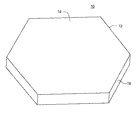
This invention features an active hybrid optical component 10, Fig. 1,
including substrate 12, typically silicon carbide or an equivalent, such as
metal, glass,
ceramic, polymer and components thereof including but not limited to a Fused
Silica,
ULE, beryllium, Zerodur, Al 6061-T6, MMC 30% SiC, Be 1-70. Be I-220-H, Cu
OFC, Cu Glidcop, Invar 36, Super Invar, Molybdenum, Silicon, SiC HP alpha, SiC
CA 02599003 2007-08-22
WO 2006/078647 PCT/US2006/001586
6
CVD beta SoC RB 30% Si, C/SiC, SS 304, SS 416, SS 17-4PH, Ti 6A14V, Gr/EP
GY70x30, metal matrix composites, carbon matrix composites, glass matrix
composites, and carbon fiber reinforced polymers having a replicated optical
surface
or film such as mirror surface 14 on one side joined to a support structure
16, on the
other side. The replicated optical surface or film 14 may include glass, Mylar
film, or
a nanolaminate such as produced by Lawrence Livermore National Laboratory, see
Nano-Laminates: A New Class of Materials for Aerospace Applications by Troy W.
Barbee, Jr., Lawrence Livermore National Laboratory, Livermore, CA 94550-9234.
These nanolaminates may be from one monolayer (0.2nm) to hundreds or thousands
of monolayers (25-100 microns) thick and are typically made from e.g.
zirconium -
copper, Invar, Monel titanium. They are generally made on a mandrel whose
surface
has been highly figured and finished so when the process is complete the
nanolaminate surface is also highly figured and finished. Thus, this substrate
no
longer need have the surface ground or polished, because the actual optical
finish, of
much higher quality, is provided by the replicated surface, e.g. a
nanolaminate.
The construction of an active hybrid optical component 10 according to one
embodiment of this invention is shown in Figs. 1 and 2, where replication film
14 is
constituted by a nanolaminate attached to substrate 12 by some means 15. The
attachment means 15 may be e.g. brazing, solder, diffusion bonding or other
bonding
such as an adhesive as hereinafter described by way of one example. The
adhesive
may include epoxies, phenolics, urethanes, anaerobics, acrylics,
cyanoacrylates,
silicones, polysulfides, elastomeric adhesives.
The support structure 16, Fig. 3, of substrate 12 may include a plurality of
major ribs 18, which intersect at a node 20 at the center of a zone of
influence. Each
CA 02599003 2007-08-22
WO 2006/078647 PCT/US2006/001586
7
major rib, such as rib 18a, includes recess or notch 22 in which an actuator
may be
located. The actuators deform substrate 16 to impose a predetermined finish
and
optical shape or figure to the replicated optical surface 14. The array of
major ribs
creates a honeycomb-like structure supporting back side 24 of surface 14 on
which
can be located cathedral ribs 26 for strengthening and further supporting
surface 14.
Actuators 30, Fig. 4, are embedded in recesses 22 of ribs 18 generally
parallel
to surface 14 and spaced from it. When operated either by extension or
contraction,
actuators 30 apply bending moments to alter the shape of surface 14, both
locally for
correctability, and globally to effect radius of curvature alterations.
Because actuators
30 act directly on the support structure in which they are embedded, in this
particular
embodiment, they require no reaction mass. In addition, even though they may
be
displacement devices, they can perform a very effective radius of curvature or
excursion shape alteration because their effect is cumulative.
Each of the actuators 30 may be an electrostrictive device or a
magnetostrictive device, a piezoelectric device or any other suitable type of
actuator
such as hydraulic, voice coil, solenoid, mechanical or phase change material
such as
shape memory alloys or paraffin. In this preferred embodiment, they are
illustrated as
electrostrictive devices of the lead-magnesium niobate or PMN type which are
preferred because they have a low thermal coefficient and very little
hysteresis and
creep and are dimensionally stable to sub-Angstrom levels. The actuators are
characteristically easy to install and replace. For example, actuator 30a,
Fig. 5, may
contain mounting tabs 32 and 34 which are receivable in mounting clips 36 and
38
mounted in notch 22b of rib 18b. Slots 36 and 38 may be mounted to rib 18b by
means of clamps 40 and 42. All of the interfaces may be supplied with an
adhesive to
CA 02599003 2007-08-22
WO 2006/078647 PCT/US2006/001586
8
permanently bond actuator 30a in position. The actuators may be ambient
temperature actuators or cryogenic actuators so that component 10 can be
converted
from one type of operation to another quite easily by simply removing one type
and
replacing it with the other.
Another type of actuator mounting is shown in Fig. 6 where a three step
installation is shown beginning with the actuator 30c being supplied with
bonding tabs
32c and 34c which may be glued to it. This assembly is then installed in
recess 22c of
major rib 18c by engaging the slots 40 and 42 in tabs 32c and 34c with the
edges of
recess 22c so that the final assembly appears as at 50 in Fig. 6. Again, some
or all of
the engagements may have an adhesive applied to bond the components.
The efficacy of this construction is illustrated in Figs. 7, 8, and 9. In Fig.
7 the
trade-offs with respect to stiffness are displayed where it can be seen that
for a design
window 52, Fig. 7, defining an areal density of 10 kg/m2 or less, a high
stiffness of
1.0E+06 inch pounds can be achieved in conjunction with that low areal density
while
maintaining a fairly high 300 Hz natural frequency. Fig. 8 illustrates the
trade-offs
with respect to excursion where the surface deformation associated with
excursion
and gravity sag are both in satisfactory ranges expressed in sectional
stiffness in inch
pounds. The trade-off with respect to correctability is demonstrated in Fig. 9
where
the correctability is plotted against Zernike polynomials indicating that the
localized
correction or correctability performs quite well even at high Zemike
polynomials with
adequate numbers of actuators. And adequate numbers of actuators is not a
problem
as they are small, lightweight, and can be highly densely packed.
Although the support structure shown is a honeycomb-like structure formed
from the intersecting ribs, this is not a necessary limitation of the
invention. For
CA 02599003 2007-08-22
WO 2006/078647 PCT/US2006/001586
9
example, in Fig. 10 the support structure on back surface 24a of surface 14
constitutes
spaced bumps or dimples or posts 60 and the actuators 30d are connected
between
pairs of posts effecting the bending moments and creating the nodes as
previously
explained with respect to the honeycomb structure.
Any suitable hardware or software system may be used to monitor and
feedback control signals to the active hybrid optical component according to
this
invention. One suitable system is illustrated in Fig. 11 by way of example and
not
limitation. There microprocessor 70 drives I/O device 72 to provide voltages
to
actuators 30'. The wavefront sensor 74 such as, a Zygo imaging device or a
Hartmann
wavefront sensor, monitors mirror surface 14, Fig. 1. Microprocessor 70 is
configured with software to establish a reference figure 76 and then establish
for each
actuator an influence function on its associated nodes or zones 78. Mirror
surface 14
is then exposed to a distorting environment 80 and once again measured in step
82.
The reference is then subtracted from the measurement to get residual error 84
and the
residual error is decomposed 86 into actuator commands which are then applied
88
through I/0 device 72 to provide the proper voltages to actuators 30'. This
routine is
carried out repeatedly in order to keep the mirror at the optimum shape or
optical
figure.
While thus far the actuator mechanism has been shown as using parallel
oriented actuators embedded in the support structure and requiring no reaction
mass
this is not a limitation of the invention. Active hybrid optical components
10e, Fig.
12, may include a replicated optical surface, e.g. 14e on substrate, face
sheet 12e,
deformable by transverse actuators 30e mounted on reaction mass 31.
Alternatively,
Fig. 13, face sheet 12f with replicated optical surface 14f can be edge driven
by
CA 02599003 2007-08-22
WO 2006/078647 PCT/US2006/001586
actuators 30f about a central support 33.
A method of making an active hybrid optical component according to this
invention particularly using a nanolaminate is described in Figs. 14 - 26
following.
There is shown in Fig. 14 a mandre1110 which contains on it a nanolaminate
112 made of, for example, zirconium-copper, Invar, Monel titanium which may be
made or may be procured from, for example, Lawrence Livermore National
Laboratory. Nanolaminate 112 may be attached to mandre1110 by means of a
parting
layer, such as carbon. Substrate 114, Fig. 15, may be a passive substrate or
an active
one as depicted in Figs 1, 3 -11, supra. Such technology is also discussed in
the form
of an active substrate used in an integrated meniscus mirror described in U.S.
Patent
Application No. 10/730,412, filed December 8, 2003, Mark A. Ealey, entitled
Integrated Zonal Meniscus Mirror, which is herein incorporated in its entirety
by this
reference. Mandre1110 with nanolaminate 112 is placed on the table 116, Fig.
16, of
a robot machine 118 such as an A&M Saga 5x52 positioning machine.
In accordance with this invention, the substrate 114, Fig. 17, is held
suspended
from the arm 122 of robot machine 118 over and aligned with nanolaminate 112
on
mandrel 110. And the two are joined in a suitable way as described above but
in this
illustrated example bonding by adhesive is preferred. An adhesive is placed
between
the confronting surfaces of substrate 114 and nanolaminate 112, then the two
parts are
brought together, the adhesive is distributed over the face and bonding
begins. After a
period of curing at room temperature, the bonded assembly 120 is put into a
temperature chamber where it is cycled, Fig. 18, first to a higher
temperature, typically
room temperature to 50 C to complete the curing of the adhesive, typically an
epoxy
such as #301-2 made by Epoxy Technology Inc., Billerica, MA or a special order
CA 02599003 2007-08-22
WO 2006/078647 PCT/US2006/001586
11
adhesive #52-180-1 made by Epoxy Technology, Tnc. Billerica, MA. After the
curing
is complete, the bonded assembly is brought down to room temperature then
raised
again to an elevated temperature, typically room temperature to 50 C and then
brought
down to a reduced temperature, typically room temperature to -20 C. This
temperature cycling induces thermal moments in the bonded assembly 120 which
enables the nanolaminate to separate from the mandrel on which it was
introduced but
remain bonded by means of the adhesive to the substrate 114. The end product
is a
hybrid optical component, mirror 126, Fig. 19, which includes the substrate
114 with a
nanolaminate 112 adhered to it.
In this way, in accordance with this invention, then, the highly polished,
high
quality optic surface provided by the nanolaminate 112 removed from mandrel
110
provides a very high quality optic, while the substrate 114 provides the
required
stiffiiess with very little weight. In addition, since the substrate 114 can
be an active
substrate, such as referred to above, any deformities in the shape or figure
of the
mirror can be easily accommodated. Further, a number of such mirrors can be
made
easily and quickly using the same mandrel. That is, the mandrel finish will
provide a
high quality optical surface on the nanolaminate for many, many forming
operations.
In the neighborhood of 40 or 50 nanolaminates with high quality optical
finishes can
be made from a single mandrel before the mandrel has to be resurfaced. The
disclosure of the active substrate in U.S. Patent Application No. 10/730,412,
filed
December 8, 2003, Mark A. Ealey, entitled Integrated Zonal Meniscus Mirror
referred to herein above with its active surface segments can be used here as
the active
substrate, with, for example, a 25 micron surface finish and then have a
nanolaminate
of perhaps 0.2 micron finish adhered to it.
CA 02599003 2007-08-22
WO 2006/078647 PCT/US2006/001586
12
The temperature cycling of the bonded assembly 120 is depicted in Fig. 20,
where it can be seen that the mandrel and nanolaminate remain generally at
room
temperature as shown at 130, Fig. 20, right through the initial bonding at
132. After a
three day cure, 134, the temperature is raised to approximately room
temperature to
50 C as at 36 to further cure the epoxy adhesive. The bonded assembly is then
reduced to room temperature as at 138 and then less than a day later once
again raised
to approximately room temperature to 50 C at 140. Following this the release
cycle
occurs wherein the bonded assembly is reduced in temperature to somewhere
between
room temperature and -20 C. At this point the nanolaminate releases from the
mandrel due to the thermal moments induced by the temperature cycling but
remains
attached by the adhesive to the substrate.
An abbreviated depiction of the steps of the method according to this
invention
are shown in Figs. 21 - 24. Initially, Fig. 21, substrate 114 is gripped by
the arm 122
of the robot machine such as for example by using holders e.g. suction cups
150. A
drop of adhesive 152 is placed on nanolaminate 112 which is carried by mandrel
110.
Arm 122 then brings down substrate 114, Fig. 22, to confront nanolaminate 112.
Adhesive 152 is now spread out over both confronting surfaces. Typically the
.force
applied is approximately 70 pounds by arm 122 and then a few more pounds,
e.g., 10
to 20, will be added manually using small weights, for example, to bring the
adhesive
to a uniform gap, preferably at about 2 . When the adhesive 152 is squeezed
out to a
chosen uniformity the entire bonded assembly as shown in Fig. 23 is cured,
first at
room temperature and then at the elevated temperature. The bonded assembly is
then
submitted to a cycle of temperature e.g., typically an elevated temperature
followed by
a reduced temperature which induces thermal moments that cause the
nanolaminate
CA 02599003 2007-08-22
WO 2006/078647 PCT/US2006/001586
13
112 to release from mandrel 110, Fig. 24, but remain adhered to substrate 114.
Adhesive 152, Fig. 25, performs the fiinction of adhering nanolaminate 112 to
substrate 114, but it also acts to fill and smooth the final surface of
nanolaminate 112
when it is adhered to substrate 114 and released from mandre1112. Typically
substrate 112 for this method does not require a lot of final finishing. A
finish, for
example, of 25 on its surface will be sufficient: contrast this with
nanolaminate 112
whose finish imbued by mandrel 112 may be in the range of 0.2 microns. Were it
not
for the adhesive, nanolaminate 112 would approach, to some level, the
roughness of
substrate 114. However, adhesive 152 not only fills the gap, but creates a
mitigating
medium that tends to average out the roughness associated with substrate 114
and
more nearly produce the smoothness inherent in nanolaminate 112. To accomplish
this adhesive 152 contains particulate material, in this preferred embodiment
fused
silica, in the epoxy medium. The fused silica may have a size, for example, of
0.8
microns for a 2.0 micron adhesive layer and the adhesive as indicated can be a
#301-2
made by Epoxy Technology, Inc. Billerica,lVlA. or it can be a special adhesive
52-180-
1 made by Epoxy Technology, Inc., Billerica, MA which already has a
particulate
material in it. The particular material used, whether fused silica or other,
and the size
of the particulate material as well as the viscosity of the epoxy as applied
and the
homogeneity of the mixture are all iunplicated in providing the smooth
attachment of
the nanolaminate 112 to substrate 114. Other desirable qualities of the
gradient
adhesive interface appear to be that it is compliant, experiences low volume
change
during curing, has minimal distortion and a good matching co-efficient of
thermal
expansion. The combination of these things in the adhesive has only been
empirically
achieved and will vary depending upon the roughness of the surfaces, the type
of
CA 02599003 2007-08-22
WO 2006/078647 PCT/US2006/001586
14
epoxy used, the gap desired, and perhaps even other parameters not yet
identified.
Additionally a commonly used layer, known as a parting layer, 153 is shown.
This
layer functions to releasably attach the nanolaminate 112 to mandrel 110. This
is well
known in the art and the materials that are used for this typically include
carbon. The
final force applied to close substrate 114 on nanolaminate 112 is guided by
the use of
a number of displacement dial meters 160, Fig. 26A, which may be mounted with
holder 162 suspended from ann 122 not visible in Fig. 26A but visible in Fig.
26B.
Ami 122, Fig. 26B, lifts substrate 114 which is shown with weighted insert 115
having holes to accommodate holders 150 and dial meters 160. Arm 122, Fig.
26C,
traverses to locate substrate 114 over nanolaminate 112. Then after the
adhesive is
applied, ann 1221owers, Fig. 26D, substrate 114 to nanolaminate 112.
Additional
weights 161, Fig. 26E, are added as indicated as necessary by dial meters 160
to
produce a force on substrate 114 to result in a desired adhesive gap width and
uniformity.
The metrology and the actual feed back and operation of the independent
actuatable portions of actuatable substrate 114 do not form a part of this
invention and
can be done in any suitable fashion, examples of this may be understood frorn
U.S.
Patent Application No. 10/936,229 filed on September 8, 2004, entitled
Adaptive
Mirror System, by Mark A. Ealey and U.S. Patent Application No. 10/935,889
filed
on September 8, 2004, entitled Integrated Wavefront Correction System, by Mark
A.
Ealey, each of them herein incorporated in its entirety by this reference. The
actuators
may be any suitable kind, such as those shown in U.S. Patent Application No
10/730,514, filed December 8, 2003, entitled, Transverse Electrodisplacive
Actuator
Array, by Mark A. Ealey and U.S. Patent Application No. 10/914,450, filed on
August
CA 02599003 2007-08-22
WO 2006/078647 PCT/US2006/001586
9, 2004, entitled, hnproved Multi-Axis Transducer, by Mark A. Ealey, each of
them
herein incorporated in its entirety by this reference.
Although in this particular example the optic is a mirror, the invention is
not
limited to only that type of optic element. In accordance with this method
then, by
freeing the nanolaminate from the mandrel, in this way, and bonding it to a
substrate
there has been obtained an optical element with high strength and stiffness,
low
weight and a high quality optical surface finish. In addition if the substrate
is an
actuatable substrate then the preparation of the substrate can be minimal as
the
finished product can be metered and then the proper pattern of actuation
imposed on
the actuatable substrate to bring the final optical surface into complete
conformity
with the desired optical figure or form.
Although specific features of the invention are shown in some drawings and
not in others, this is for convenience only as each feature may be combined
with any
or all of the other features in accordance with the invention. The words
"including",
"comprising", "having", and "with" as used herein are to be interpreted
broadly and
comprehensively and are not limited to any physical interconnection. Moreover,
any
embodiments disclosed in the subject application are not to be taken as the
only
possible embodiments.
In addition, any amendment presented during the prosecution of the patent
application for this patent is not a disclaimer of any claim element presented
in the
application as filed: those skilled in the art cannot reasonably be expected
to draft a
claim that would literally encompass all possible equivalents, many
equivalents will
be unforeseeable at the time of the amendment and are beyond a fair
interpretation of
what is to be surrendered (if anything), the rationale underlying the
amendment may
CA 02599003 2007-08-22
WO 2006/078647 PCT/US2006/001586
16
bear no more than a tangential relation to many equivalents, and/or there are
many
other reasons the applicant can not be expected to describe certain
insubstantial
substitutes for any claim element amended.
Other embodiments will occur to those skilled in the art and are within the
following claims.
What is claimed is: