Note: Descriptions are shown in the official language in which they were submitted.
CA 02599696 2007-08-30
WO 2006/092052 PCT/CA2006/000304
1
FABRY-PEROT OPTICAL SENSOR
AND METHOD OF MANUFACTURING THE SAME
FIELD OF THE INVENTION
The present invention relates to the field of optical sensors and more
particularly
concerns a miniature Fabry-Perot sensor which is robust and easy to
manufacture.
BACKGROUND OF THE INVENTION
Fiber optic pressure sensors have been topic of intense research during the
last
decade as they can be made very small, compact, immune to electromagnetic
interference, biocompatible and can be used at elevated temperature or in a
harsh
chemical environment. Applications for such sensors are therefore numerous and
range from combustion and jet engine controls to biomedical applications.
It is known in the prior art to provide pressure sensors at the tip of an
optical fiber.
For example, published international patent application no. WO 02/23148
(WILNER et aL) shows a housing made from silicon in which the end section of a
lead fiber and a silicon diaphragm are fixed. The flat cleaved lead fiber end
and
the diaphragm form two reflective surfaces that define a Fabry-Perot
interferometer. The optical signal from the lead optical fiber is split into
two paths
which mutually interfere. The sum of their interference is function of the
distance
between the fiber end and the diaphragm position, the latter being a function
of
pressure.
Other sensors of this type are for example described in patents and patent
applications EP 1 089 062; US 4,491,590; US 5,381,229; US 6,539,136; US
5,657,405; US 6,597,820; US 6,820,488; US 6,823,738; US 2004/0223679; US
2005/0041905; WO 99/45352 and WO 02/23148. The following publications may
also be consulted: MacPherson W.N. et al., "Miniature fiber optic pressure
sensor
for turbomachinary applications", Rev. Sci. Instr., 1999, Vol. 70 n 3, pp.
1868
1874,), Pinet E. at aL "Miniature fiber optic pressure sensor for medical
CA 02599696 2007-08-30
WO 2006/092052 PCT/CA2006/000304
2
applications: an opportunity for intra-aortic balloon pumping (IABP) therapy',
Proc.
of SPIE, 2005, Vol. 5855, pp. 234-237. For all the solutions mentioned in
these
documents, the typical design produces a sensor that is larger than the
diameter
of the lead optic fiber used for its interrogation.
U.S. patents no. 4,078,432, US 4,701,614, US 4,918,305 and US 5,193,129
describe small micro-binding fiber optic pressure sensors. In all cases, two
optical
fibers are needed; one for the probing light and the other for the detected
light
whose intensity is dependent on the pressure applied on the sensor.
European patent EP 0 503 812 discloses a small fiber optic pressure sensor
using
fluorescence-quenching, suitable for example for arterial blood pressure
measurements. The size of such a sensor could be made very close to the
optical
fiber diameter.
There are very few known devices where the sensor diameter is equal to the
diameter of the lead optical fiber. Some examples could be found in patents
and
patent applications EP 0 997 721, US 2004/0114848. These technologies however
have their drawbacks; for example, in EP 0 997 721 the manufacturing procedure
is relatively complicated and requires application of special tools and
materials. In
US 2004/0114848, the intrinsic Fabry-Perot sensor includes a thin film
sandwiched
between two fiber ends.
Other ultra-miniature pressure sensors have been reported in the literature.
The
paper by Cibula & Donlagio "Miniature fiber-optic pressure sensor with a
polymer
diaphragm", Appl. Opt. 2005, Vol. 44 n 14, pp. 2736 2744, and Slovene patent
SI
21242 disclose a fiber optic pressure sensor with a polymer diaphragm that is
not
larger than the size of the optical fiber. Papers by Abeysinghe D.0 at al. ("A
novel
MEMS pressure sensor fabricated on an optical fiber', IEEE Phot. Tech. Lett.,
2001, Vol. 13 n 9, pp. 993 995,), Abeysinghe D.0 et al. ("Novel MEMS pressure
and temperature sensors fabricated on optical fibers" J. Micromech. Microeng.
CA 02599696 2007-08-31
PCT/CA 2 00 6 / 0 0 0 3 0 4
02 JANUARY Z0017 0 2 0 1 2 0 0 7
3
2002, Vol. 12, pp. 229 235,) and Totsu K. et al. ("Ultra-miniature fiber-optic
pressure sensor using white light interferometry", J. Micromech. Microeng.,
2005, Vol. 15, pp. 71 75,) all disclose pressure sensors manufactured at the
tip
of a lead optical fiber using photolithographic patterning techniques.
Other embodiments of miniature sensors are shown in U.S. patent application
no. 2005/0062979 (ZHU et al.). The miniature sensor of Zhu is designed by
bonding a hollow tube to a lead fiber end-face and then bonding a diaphragm to
the hollowed tube to create a Fabry-Perot interferometer. Identical
configurations, employing polymer diaphragm, was also reported by Cibula E. et
al. ("Miniature fiber optic pressure sensor for medical applications", Proc.
IEEE
Sensors 2002, Vol. 1 n 12-14 pp. 711-714,) and in Slovene patent SI 21242.
One drawback of such sensors is the relative fragility of the hollow spacer,
both
during the manufacturing of the spacer and during its use.
There is therefore a need for a miniature optical sensor which alleviates
drawbacks of the prior art.
SUMMARY OF THE INVENTION
In accordance_ with a first aspect of the present invention, there is
therefore
provided an optical sensor for sensing a parameter, said optical sensor
comprising:
a lead optical fiber;
a spacer of similar transversal dimensions than the lead optical fiber, said
spacer being supported by said lead optical fiber, and projecting strictly
forward therefrom, said spacer having an end surface curving inwardly
from a forward end of said spacer opposite said lead optical fiber; and
a diaphragm extending across said forward end of the spacer, said
diaphragm being flexible in response to said parameter, said diaphragm
defining a forward reflector of a sensing Fabry-Perot cavity within said
optical sensor.
AMENDED SHEET
CA 02599696 2007-08-31
PCT/CA 2 0 0 6 / 0 0 0 3 0 4
o2 JANUARY 2007 0 2 0 1 0 0 7
=
=
4
In accordance with another aspect of the invention, there is also provided a
method for manufacturing an optical sensor for sensing a parameter, said
method comprising the steps of:
a) providing a spacer optical element of similar transversal dimensions than
the lead optical fiber, said spacer being supported by said lead optical
fiber and projecting strictly forward therefrom;
b) shaping a forward end of said spacer optical element to define a spacer
having an end surface curving inwardly from a forward end of said spacer
opposite said lead optical fiber;
c) permanently joining a diaphragm optical element to said forward end of
the spacer; and
d) shaping said diaphragm optical element to define a diaphragm extending
across said forward end of the spacer, said diaphragm being flexible in
response to said parameter, said diaphragm defining a forward reflector
of a sensing Fabry-Perot cavity within said optical sensor.
The present invention advantageously provides Fabry-Perot sensors where the
'
sensing elements may have a diameter as small as the lead optical fiber
diameter, hence the reference to a miniature device. The parameter the sensor
is sensitive to may for example be pressure, force, acceleration, acoustic
waves,
vibrations or combinations thereof. The present invention can be particularly
useful for applications where the reduced size, electromagnetic interference
(EMI) insensitivity, high thermal stability and low drift are important
concerns.
Other features and advantages of the present invention will be better
understood
upon reading of preferred embodiments thereof with reference to the appended
drawings.
BRIEF DESCRIPTION OF THE DRAWINGS
FIG. 1 is a cross-sectional side view of an optical sensor according to a
preferred embodiment of the invention.
FIGs. 2A to 2F show different steps of a method for manufacturing an optical
sensor as shown in FIG. 1.
AMENDFD SHEET
=
CA 02599696 2007-08-30
WO 2006/092052 PCT/CA2006/000304
FIG. 3 is a schematized illustration of an experimental set-up to perform a
polishing step according to a preferred embodiment of the invention.
FIG. 4 is a schematized illustration of an experimental set-up to perform an
etching
5 step according to a preferred embodiment of the invention.
FIGs. 5A to 5E are cross-sectional side views of optical sensors having
spacers
with curved surfaces of different profiles according to preferred embodiments
of
the invention.
FIGs. 6A to 6C are cross-sectional side views of optical sensors having
different
spacer shapes according to preferred embodiments of the invention.
FIGs. 7A to 7D are cross-sectional side views of optical sensors having
different
diaphragm shapes according to preferred embodiments of the invention.
FIGs. 8A to 8E. show different steps of a method for manufacturing an optical
sensor according to another embodiment of the invention.
FIG. 9 is a cross-sectional side view of the optical sensor of FIG. 1 packaged
in a
protective tubing according to another embodiment of the invention.
FIG. 10 is a schematized illustration of an experimental set-up to perform an
interrogation of an optical sensor according to an embodiment if the
invention.
FIGs. 11 and 12 are graphs showing experimental results obtained for two
optical
sensors according to preferred embodiments of the invention.
DESCRIPTION OF PREFERRED EMBODIMENTS OF THE INVENTION
In the following description, similar features in the drawings have been given
similar reference numerals and in order to weight down the figures, some
CA 02599696 2007-08-30
WO 2006/092052 PCT/CA2006/000304
6
elements are not referred to in some figures if they were already identified
in a
precedent figure.
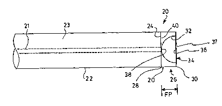
With reference to FIG. 1, there is shown an example of an optical sensor 20
according to an embodiment of the present invention. The sensor of the present
invention is meant for sensing a given parameter. The parameter may be
physical
or chemical and may for example be embodied by pressure, force, acceleration,
acoustic waves, vibrations, combinations thereof, or any other parameter apt
to
induce a displacement of a diaphragm as will be seen further below.
Optical sensor
The optical sensor 20 of FIG.1 first includes a lead optical fiber 22 having
an end
face 24. The lead optical fiber preferably has a core 21 and a cladding 23,
and is
apt to guide a light signal towards its end face 24 and guide the reflected
light back
in the opposite direction. It will be clear to one skilled in the art that the
designation
of "lead" optical fiber refers to the use of this fiber as a conduit for the
sensing light
signal and is not meant as representative of any particular property of the
optical
fiber itself. The lead optical fiber may be single mode or multimode, and may
be
made of any suitable materials such as pure silica, doped silica, composite
glasses or sapphire.
The optical sensor 20 further includes a spacer 26 projecting forward from the
lead
optical fiber 22. The spacer 26 preferably has a rearward end 28, which
preferably
defines a substantially flat rearward boundary 40 permanently joined to the
end
face 24 of the lead optical fiber 22. It will be understood that the adjective
of "flat"
is used herein in the general sense as opposed to a "curved" surface, and that
in
practice the rearward boundary may have imperfections which do not
substantially
affect the operation of the sensor. The spacer 26 further has an end surface
32
which curves inwardly from the forward end 30 of the spacer 26 opposite the
lead
optical fiber 22. The designations of "rearward" and "forward" are used
throughout
the present specification to refer to the orientation of components with
respect to
CA 02599696 2007-08-30
WO 2006/092052 PCT/CA2006/000304
7
light coming from the lead optical fiber 22, and are not indicative of any
preferential
direction.
The end surface 32 is understood to be the surface of the spacer 26 facing the
forward end thereof. The expression "curves" is understood as referring to a
surface that deviates from planarity in a generally smooth, continuous
fashion, and
the adjective "inwardly" simply refers to the inside of the spacer. The actual
curve
defined by the end surface 32 may have a variety of profiles.
The optical sensor 20 further includes a diaphragm 34 extending across the
forward end 30 of the spacer 26. The diaphragm 34 is preferably a thin
membrane
and is flexible in response to the parameter to be analyzed. Preferably,
either the
front 37 or rear 36 surface of the diaphragm 34 forms a reflector of a Fabry-
Perot
cavity. Alternatively, if the diaphragm is thin enough, the reflection from
the
forward reflector can be observed as the sum of reflections at each of the
front 37
and rear 36 surfaces of the diaphragm. This situation can be treated either as
a
double Fabry-Perot cavity or as a single cavity, as reflected light waves from
both
surfaces will add coherently. The final effect is that the reflected wave
encounters
a phase shift different from 180 degrees upon reflection, which in general
does not
require the use of a special signal processing to measure the desired
parameter(s). The other reflector of this cavity is preferably embodied by
either the
end face 24 of the lead fiber 22 or the inwardly curved end surface 32 or the
spacer 26. In the latter case, the spacer could be an integral part of the
lead
optical fiber itself, its extremity having been given the appropriate shape.
By
definition, a reflector of a Fabry-Perot cavity has reflective or semi-
refrective
properties. These properties may simply come from the interface between two
different media, or be advantageously improved by providing a semi-reflective
layer coating onto the appropriate surface. The surface of the diaphragm 34
defining the reflector on the diaphragm side of the cavity may also
advantageously
be coated with a fully reflective layer to increase light reflection.
CA 02599696 2007-08-30
WO 2006/092052 PCT/CA2006/000304
8
A deflection of the diaphragm can be measured for example on the basis of
interference of reflected light in the Fabry-Perot cavity, and an appropriate
optical
signal processing system can deduce therefrom a variation in the measured
parameter. The optical processing of the signal is adapted to the
characteristics of
the Fabry-Perot cavity. It will be understood by one skilled in the art that
the
different interfaces in the sensor may defined more than one Fabry-Perot
cavity,
and that appropriate signal processing will select the light from desired one.
Alternatively, the light reflected within more than one pair of reflectors,
defining
plural Fabry-Perot cavities, may be resolved to extract information from each
of
them or from the resulting combination of them. Sensing by a Fabry-Perot
cavity
and appropriate signal processing techniques are well known to those skilled
in
the art and need not to be described further here.
The use of a spacer having a profile as described above, especially provided
with
an inwardly curved end surface, between the lead optical fiber and the
diaphragm
ensures a good dimensional stability of the sensor structure during its
manufacturing, as will be seen further below. In addition, the provision of a
spacer
having thicker walls as a result of its inwardly curved shape has been proven
to be
more dimensionally stable. This makes the optical sensor according to the
present
invention more robust during manufacturing, packaging and final use.
The curved end surface 32 of the spacer 26 may take any appropriate shape. In
the embodiment of FIG. 1, it generally defines U-shape and its innermost point
38
reaches the rearward boundary 40 of the spacer 26 at its rearward end 28.
Other
exemplary spacers 26 having U-shaped and V-shaped profiles are shown in FIGs.
5A to 5E. For example, FIG. 5A shows a spacer 26 having a curved end surface
32 reaching the rearward boundary, similarly to the sensor of FIG. 1. This
particular embodiment is preferred for sensors using a single mode lead
optical
fiber 22. The spacer 26 of FIG. 5B has a curved end surface 32 whose innermost
point 38 extends forward of the rearward boundary 40. FIG. 5C shows a spacer
26
where the curved end surface 32 begins at a certain distance inside the
cavity, the
CA 02599696 2007-08-30
WO 2006/092052 PCT/CA2006/000304
9
space 26 thereby defining a tubular portion 31 at its forward end 30. In the
embodiment of FIG. 5D, the bottom of the U shape defined by the curved end
surface 32 intersects the rearward boundary 40. The embodiment of FIG. 5E
shows a V-shaped curved end surface 32.
In several preferred embodiments of the invention, the spacer has a diameter
substantially equal to the diameter of the lead optical fiber. For some
applications,
especially those requiring a higher sensitivity of the sensor, the spacer 26
may
have a diameter larger than that of the lead optical fiber 22, as for example
shown
in FIG. 6A. In the embodiment of FIGs. 6B and 6C, the curved end surface 32 of
the spacer 26 defines a shape reminiscent of a W. According to this
embodiment,
the spacer 26 form a protuberance extending forward from its central portion,
this
protuberance defining a micro-lens 42 in the center of the Fabry-Perot cavity
that
can focus or collimate light preferably to the inner surface 36 of the
diaphragm 34.
In the embodiment of FIG. 60, an additional spacer 44 is provided between the
spacer 26 and lead fiber 22, to ensure a proper geometry of the optical setup
and
to achieve appropriate focusing or collimation of the sensing light within the
Fabry-
Perot cavity.
Referring to FIGs. 7A to 7D, it can be seen that the shape of the diaphragm 34
itself may also be used to provide additional advantageous features according
to
other variants of the present invention. For example diaphragms 34 with non-
uniform or corrugated surfaces could be used. Corrugated diaphragm can provide
a higher overall sensitivity of the corresponding optical sensor 20 and relax
internal stress leading to better sensor stability. For instance, the
diaphragm 34
may be provided with a protuberance 46 protruding from its central portion as
shown in FIGs. 7B, 7D (protruding forward only) and 7C (protruding both
rearward
and forward). Such protuberance 46 may advantageously act as an inertial
member, making the optical sensor 20 more sensitive to axial acceleration, to
acoustic waves or to vibrations. The protuberance 46 is preferably defined by
an
increased thickness of the diaphragm 34 in its central portion. The presence
of this
CA 02599696 2007-08-30
WO 2006/092052 PCT/CA2006/000304
protuberance 46 can also help to reduce deformations in the central portion of
the
diaphragm 34 so that it retains a more or less flat surface, especially when
the
diaphragm 34 is deflected, that helps to maintain the visibility of the Fabry-
Perot
within the whole range of the operation of the optical sensor 20.
5
The shape of the diaphragm 34 may also be selected to form a protective hollow
member 48 projecting forward of the diaphragm, as shown in FIGs. 7A and 7D.
The hollow protective member 48 and diaphragm preferably form a monolithic
structure. Such a protective hollow member 48 could advantageously protect the
10 diaphragm 34 from mechanical stresses that could occur during sensor
packaging
or during normal use of the sensor.
Referring to FIG. 9, in accordance with another embodiment of the invention,
the
optical sensor according to any of the variants discussed above may be
packaged
in a protective tubing 50, preferably of a size comparable to that of the
optical
sensor. The protective tubing may be made of metal, polymers or any other
appropriate material. Such tubing is preferably flexible but may also be
rigid,
especially for applications where an ultra-miniature size is not a critical
issue. As
shown in FIG. 9 the optical sensor 20 is preferably slightly retracted inside
the
protecting tubing 50, not too far from its opening in order to allow stimulus
transduction to the sensor while offering an improved protection. The
protective
tubing may enclose the optical sensor 20 partially or completely, and
preferably
encloses the entire sensor and a section of the lead optical fiber. It may be
filled
with a substance 52 selected to transduce the external stimulation to be
detected
by the sensor while still providing an additional protection for the most
fragile
exposed parts thereof. Example of appropriate substances include a flexible
polymer such as polyurethane, soft rubber or the like, a gel such as silicone
gel or
hydrogel or the like, a liquid such as mineral or organic oils, water or other
appropriate liquids such as the ones with high viscosity, with high surface
tensions
or liquids or polymers that will preferably not be dissolved in the external
medium
where the disclosed sensor will be used. For liquids, it is worth mentioning
that
CA 02599696 2007-08-30
WO 2006/092052 PCT/CA2006/000304
11
due to the ultra-miniature size of the sensors obtained in numerous
applications of
the present invention, the liquids could easily remain trapped inside the
protecting
tubing simply due to surface tensions and capillary effects. The selection of
appropriate liquids and appropriate protecting tubing material will thus be
oriented
preferably in order to maximize those effects, thereby keeping the substance
inside the protecting tubing. It is worth mentioning that in some cases,
especially
those involving flexible polymers, the substance 52 can also act as protecting
tubing 50 providing additional protection for the optical sensor tip while
insuring
also transduction to the sensor 20 of the external stimulation.
io
As will be further explained below, the manufacturing of optical sensors
according
to the present invention preferably include fusion splicing of the different
components, which occurs at elevated temperature where the polymeric cladding,
that usually protects the commercially available optical fibers, can not
survive. As
is a consequence, when using standard fusion splicers there is usually at
least about
0.3 to 1 cm of optical fiber that is stripped from its polymeric buffer that
usually
protects mechanically the glass from scratches and micro-cracking. It thus
worth
mentioning that the transduction substance could also advantageously be used
to
protect the sensor and the most fragile part of the tip of the lead optical
fiber.
20 Substances that do not degrade the material of the lead optical fiber
should thus
preferably be selected.
It is additionally worth mentioning that the protective packaging mentioned
above
could also present interesting advantages for good stimulus transduction with
25 increased protection of the sensitive and likely to be fragile part of
the sensor.
When used in a packaging similar to the one shown in FIG. 9, the optical
sensor
could readily be used as a micro-pressure or micro-force sensor. The portion
between the sensor tip and the protective tubing could act as a buffer section
against stimulus which otherwise would have been exceeding the range of the
30 sensor, and could have caused its destruction.
CA 02599696 2007-08-30
WO 2006/092052 PCT/CA2006/000304
12
The additional protective packaging could finally advantageously be well
suited to
applications such as for instance medical applications where the size of the
sensor, its immunity to EMI, its high sensitivity as well as its low drift are
crucial
advantages. A potential very interesting application of such packaging would
be
for instance ultra-miniature instrumented catheters suitable for instance for
paediatric or small animals' surgery applications. It is worth mentioning that
other
additional protective packaging could be designed and used in other
applications
without limiting the scope of the described preferred packaging and
application.
Alternatively other similar designs may for instance be implemented where the
end-tip of the package could be filled with a substance that swells or shrinks
in
presence of a given analyte, such as hydrogels or similar products capable of
swelling in presence of water or possibly organic vapors. Such packaging,
possibly
modified compared to what is schematically illustrated in FIG. 9, could thus
be
used to make the ultra-miniature Fabry-Perot fiber optic sensor described in
the
present invention, sensitive to humidity or volatile organic compounds.
Numerous
designs and applications could be derived from this concept such as for
instance
the use of a substance that swell or shrink with temperature variations, hence
making the sensor sensitive to temperature. Different transduction mechanisms
could be used to make the sensor sensitive to other stimuli.
Each of the lead optical fiber, the spacer and the diaphragm may
advantageously
be made from pure silica, doped silica glass, composite glass as well as from
sapphire, the latter being particularly suitable for extreme high temperature
applications.
The design and characteristics of a given optical sensor according to the
present
invention are preferably tailored to the target application thereof. Highly
sensitive
sensors suitable for measurements of lower and higher industrial pressures may
be achieved. A glass-only sensor designs allow for good temperature and
chemical stability and provide resistance to other environmental influences.
Since
CA 02599696 2007-08-30
WO 2006/092052 PCT/CA2006/000304
13
the materials suggested above are inert and very stable, extremely low drift
with
time, outstanding accuracy and consistent sensor performances are achievable.
Due to the small size and the nature of these materials, the resulting sensor
presents low temperature dependence. This feature is of particular interest
not
only for applications where a miniature size is essential, but also where
sensor
stability and precision are crucial. As this is the case for all fiber optic
sensors,
optical sensors according to the present invention are completely insensitive
to
electromagnetic interferences and are intrinsically safe. They therefore could
operate perfectly in electromagnetic noisy or hazardous environments such as
encountered in numerous industrial, chemical or medical applications. Sensors
according to the present invention can also be well suited for demanding
applications such as oil well down-holes or jet engines pressure monitoring
where
high pressure and temperature are present. They could be also very useful in
challenging fields such as biology (microbiology, genetics...), medicine
(paediatrics, diagnostic, patient monitoring or animal testing...), chemistry
(microwave chemistry, polymer processing...) and physics (aerospace, micro-
fluidics, micro-robotics...). As many sensors may be packed in a very small
volume, several sensors could be arrayed and, provided an adequate multi-
channels optical interrogation unit is used to read the Fabry-Perot cavities,
incredibly localized surface pressure distribution could for instance be
measured,
offering the opportunity for unique micro-sensing applications. The
applications
mentioned above are naturally non-limitative examples.
Manufacturing methods
In accordance with another aspect of the invention, there are also provided
several
variants of a method for manufacturing an optical sensor for a given parameter
as
described above.
Referring to FIGs. 2A to 2F, there are illustrated steps of a method according
to
one embodiment of the invention. The first such step, shown in FIG. 2A,
involves
permanently joining a spacer optical element 54 to the end face 24 of a lead
CA 02599696 2007-08-30
WO 2006/092052 PCT/CA2006/000304
14
optical fiber 22. As mentioned above, the lead optical fiber 22 carries a
sensing
light signal to and from the tip of the optical sensor. It is preferably
embodied by a
single mode fiber but could be multimode, and may be made of any suitable
material such as pure silica, doped silica, sapphire or composite glass. The
spacer
optical element 54 may be embodied by any element having the necessary
characteristics to be transformed through shaping into a spacer having the
profile
described above. In the preferred embodiment, the spacer optical element 54 is
a
length of optical fiber having a predetermined etchability profile. For
example, it
could be embodied by a graded index multimode optical fiber or any other glass
lo element having a suitable distribution of dopants therein. In alternative
embodiments, if the lead optical fiber has an appropriate etchability profile,
the
spacer optical element could be embodied by the extremity of the lead optical
fiber
itself.
The permanent joining of the spacer optical element 54 to the lead optical
fiber 22
is preferably achieved through splicing, which may be accomplished with a
standard optical fiber fusion splicer. Standard requirements known in the art
should preferably be maintained in order to have good splicing results. One
such
requirement consists of making sure that the end-faces of both fibers to be
spliced
should be perfectly cleaved with smooth surface perpendicular to the fiber
axis.
Both the lead optical fiber 22 and the fiber embodying the spacer optical
element
54 may for instance have an outer diameter of 125 pm or less. Larger fiber
diameters could also be used, especially if higher sensitivity is desired, as
required
for instance for medical or acoustical applications. Optionally, fibers having
different diameters could be spliced, resulting in an optical sensor such as
shown
in FIG. 6A. In that case it is usually beneficial to have a larger diameter
for the
spacer optical element since this will be helpful to increase the final wall
thickness,
to improve mechanical resistance, as well as to increase the final diaphragm
diameter for improved sensor sensitivity. For such an embodiment, a fusion
transition 56 at the interface between the two fibers may be created during
the
fusion splice. Preferably, both the lead optical fiber 22 and the fiber
embodying the
CA 02599696 2007-08-30
WO 2006/092052 PCT/CA2006/000304
optical spacer element 54 may have a diameter in the range of 50 to 500 pm,
with
core sizes between 20 and 475 pm. Fibers having .dimensions outside of those
ranges could also be used.
5 In order to improve the signal produced by the Fabry-Perot cavity of the
sensor
under manufacture, a semi reflective coating may optionally be applied on the
end
face 24 of the lead optical fiber 22 before it is joined with the spacer
optical
element 54.
10 The method of the present invention includes a second step of shaping
the
forward end 30' of the spacer optical element in order to obtain the desired
spacer
profile. Preferably, this is accomplished in two sub-steps. The forward end
30' of
the spacer optical element 54 is first cleaved to reduce its length Ls,
typically to
about 10 to 100 pm. This is illustrated in FIG. 2B. Cleaving may be performed
15 using standard cleaving mechanical tools (scribe and break, ultrasonic
cleaving,
etc.) or by other techniques known in the art, such as for example CO2 laser
cleaving techniques. With such techniques, if appropriate visual diagnostic
and
displacement tools are implemented, a precise and reproducible cleave could be
obtained, which could be very useful if batch processes are established in
order to
reduce production costs of the sensor. If the cleaved length Ls of the spacer
optical
element 54 is slightly above the appropriate targeted value, it is possible to
add a
controlled mechanical polishing step.
The second sub-step of the shaping of the forward end 30' of the spacer
optical
element 54 further involves shaping its end surface 32 so that it curves
inwardly,
as explained above. This is preferably accomplished by dipping the forward end
30' of the spacer optical element 54 in an appropriate etching medium 58
selected
as a function of the etching properties of the spacer optical element, such as
a
buffered HF and NH4F etching solution or pure HF acid, as shown in FIG. 2C.
The
etching medium may be in a liquid or gaseous phase. The spacer optical element
54 preferably has an etchability profile selected so that etching will result
in an
CA 02599696 2007-08-30
WO 2006/092052 PCT/CA2006/000304
16
inwardly curved surface having the desired shape. For example, if a standard
graded index fiber is used, the core, doped with Ge02 will etch at a much
higher
rate than the cladding, and the etching rate will be higher in the center of
the core
as the Ge02 concentration is greater there. For example, the measured etching
.. rate of the center of standard 62.5 pm multimode fiber core is about 7
pm/min, and
the cladding, generally made of pure Si02, etches at approximately 0.5 pm/min.
Parts of the core between its center and the cladding etch at proportionally
lower
etching rates than the center. The etching process could run until the
innermost
point 38 of the curved end surface 32 reaches the boundary 40 between the lead
.. fiber 22 and the created spacer 26, as shown in FIG. 2D. For some
applications, it
could be important that the etching be stopped at the moment when this
boundary
is reached as the end face 24 of the lead fiber 22 may be otherwise damaged,
resulting in a quick drop in its reflectivity. The structure obtained in this
way is
preferably neutralized and cleaned in an ultrasonic cleaner. With a preferred
.. appropriate design known in the art (Cibula & Donlagio, "Miniature fiber-
optic
pressure sensor with a polymer diaphragm", Appl. Opt. 2005, Vol. 44 n 14, pp.
2736 2744,) it is possible to continuously monitor the light reflectivity
during the
etching process in order to precisely determine when the chemical etching
should
be stopped. This may for example be achieved using appropriate optical
.. monitoring equipment connected to the lead optical fiber 22, such as shown
in
FIG. 10. The highest reflectivity is usually achieved when the innermost point
30 of
the forward end surface of the spacer is etched exactly or to sub-wavelength
distance away from the interface between the spacer 26 and the end face of the
lead optical fiber. The monitoring equipment 74 could for example be embodied
by
.. a 2x2 coupler 76 coupling the lead optical fiber 22 to other optical fibers
78, 79 and
81. The optical fiber 81 preferably has one end inserted into an index
matching gel
80 to avoid back reflections. The optical fiber 79 has one end connected to an
optical source 82, such as an accordable laser source or simply a broadband
white light source optionally coupled to a depolarizer or a filter 84. The
optical fiber
.. 78 has one end connected to a light detector 86, such as a power meter or
the
like, preferably to observe the signal reflected by the optical sensor 20 in
the
CA 02599696 2007-08-30
WO 2006/092052 PCT/CA2006/000304
17
etching medium 58. When the signal rises and achieves its maximal value, the
etching is stopped as this condition indicates that the innermost point of the
end
surface of the spacer has reached the end face of the lead fiber.
Alternatively the
etching could be stopped also when the signal reaches a given value if partial
etching is desired. If a good control of the length Ls of spacer optical
element has
been achieved in the cleaving and/or polishing sub-step (e.g. by using CO2
laser
cleaving techniques known in the art, or controlled polishing), the etching
process
could be performed in batches with only a few lead optical fibers being
monitored.
Such an arrangement could be economically very valuable.
The desired spacer profile may advantageously be obtained through the
selection,
as the spacer optical element, of a length of optical fiber having a core
provided
with a gradient distribution of dopants in the radial direction. For example,
fibers
with the graded cores doped with Ge02, TiO2, P205 or the like can be very
is selectively etched in HF acid. In these cases, the regions of the core
having the
highest concentration of dopants will etch at the highest rate. Preferably,
the
concentration of dopants is the highest in the center and decreases towards
the
edges of the core. The reversed situation is also possible, provided that an
appropriate etching solution, such as NH4F buffered HF, is selected to achieve
the
highest etching rate in regions where the lowest dopant concentration is
present.
Referring to FIG. 2E, the method of the present invention next includes a step
of
permanently joining a diaphragm optical element 62 to the forward end 30 of
the
spacer 26. The diaphragm optical element 62 may be embodied by a length of
standard or non-standard single mode or multimode fiber, with or without a
doped
core, by a doped or undoped solid rod, etc. In the preferred embodiment, the
permanent joining is accomplished by splicing, preferably with the help of a
fusion
splicer. The diaphragm will define a reflector of a Fabry-Perot cavity in the
sensor,
the other reflector of this cavity being defined by either the end face of the
lead
optical fiber or the inwardly curved surface of the spacer.
CA 02599696 2007-08-30
WO 2006/092052 PCT/CA2006/000304
18
Both reflectors of the Fabry-Perot cavity, embodied by the end face of the
lead
fiber or the inwardly curved end surface of the spacer on one side and the
rear
surface of the diaphragm optical element may be provided with a reflective
coating
prior to their respective splicing. The coating on the lead fiber side should
be semi-
s reflective, whereas the coating on the diaphragm could also be fully
reflective
coating such as the one obtained with thick metallic coating (such as Cr, Al,
Ag,
Au, Ti and the like). Such coatings that could improve the finesse or level of
back
reflected light of the FPI could be obtained using various deposition
techniques.
Thin metallic coating (e.g. titanium and the like) or preferably oxides
coating (e.g.
Ti02, Zr02, Ta205, A1203 and the like) or semiconductor thin coating (e.g.
silicon
nitride and the like) could be used for such purposes in single or multiple
layers. If
appropriately selected, such coating could also serve as chemical etch-stop
for the
next step of the process in order to avoid that the chemical etching modifies
the
first Fabry-Perot interference surface.
The present method next includes a step of shaping the diaphragm optical
element to define a diaphragm 34 extending across the forward end 30 of the
spacer 26, as shown in FIG. 2F. This may be accomplished in a variety of
manner.
In one embodiment of the invention, the shaping of the diaphragm optical
element
includes a sub-step of cleaving its forward end to a predetermined length LD,
for
example at a distance between 5 and 100 pm away from the tip of the spacer 26,
as shown in FIG. 2F. A tight control of the length LD is preferable as the
results of
this cleaving process may have an important impact on the sensor performances.
The different cleaving techniques described above in relation to the cleaving
of the
spacer optical element may again be used here for the cleaving of the
diaphragm
optical element. Different techniques may be used for cleaving different
components of a given sensor. If a good control of the cleaving is achieved,
further
shaping of the diaphragm may not be necessary and a functional sensor could be
obtained from this step. Since the minimum desired thickness of the diaphragm
obtained from cleaving is rarely bellow 2 to 5 pm (otherwise the risk of
breaking
the diaphragm during cleaving is too high and precise control over mechanical
CA 02599696 2007-08-30
WO 2006/092052 PCT/CA2006/000304
19
cleave positioning is limited), high pressure sensors (such as 0-100 MPa)
could be
produced directly at that sub-step. For increased sensitivity sensors
manufacturing, the following sub-steps are usually necessary.
The cleaving of the forward end of the diaphragm optical element may be
replaced
or followed by a mechanical polishing sub-step. Through an appropriately
controlled polishing, the length LD of the diaphragm may be reduced down to
about 1 to 5 pm. Standard polishing technique may be used with special care of
the sensitive and brittle parts of the sensor. As shown in FIG. 3, the
polishing sub-
step is preferably realized by mechanically maintaining the sensor 20 into a
fiber
optic connector ferrule 64 placed perpendicularly to a preferably rotating
polishing
surface 66 such as polishing papers of different grit-sizes. For example,
polishing
paper of 1 to 3 pm grit-sizes may be first used followed by a 0.3 to 0.5 pm
grit-size
paper for the last micron. Water, alcohol or another polishing medium 68 could
advantageously be used for a surface finish of better quality. For
measurements of
low pressures, such as for example required for most medical applications,
diaphragm thickness even smaller than achievable with the technique described
above may prove necessary. In such a case, further control of the polishing
sub-
step may be achieved by performing it in a pressurized vessel 70, and
connecting
the lead optical fiber 22 to an optical interrogation unit 72 which measures
the
response of the sensor 20 according to pressure variations imposed into the
pressurized vessel 70. The polishing sub-step is ended once the sensor
sensitivity
reaches a targeted value.
For certain pressure ranges, the controlled polishing described above may be
sufficient to shape the diagram to the desired thickness. For applications
requiring
a particularly high sensitivity, the shaping of the diaphragm may further
include an
etching sub-step. Referring to FIG. 4, an exemplary set-up for performing such
an
etching of the diaphragm optical element is shown. An appropriate etching
medium 58, such as a buffered HF and NH4F etching solution, is prepared and
the
forward end 63 of the diaphragm optical element is dipped therein. The etching
CA 02599696 2007-08-30
WO 2006/092052 PCT/CA2006/000304
medium 58 is preferably selected according to the physical characteristics of
the
diaphragm optical element. For example, if a glass rod or an optical fiber
with an
undoped core is used, the etching may be performed also in pure HF acid. It
may
alternatively be advantageous to use an optical fiber having a germanium doped
5 core as the area doped with germanium etches at a lower rate as the pure
silica
(Si02) areas. This may prevent the formation of holes in the diaphragm.
In the embodiment of FIG. 4, the lead optical fiber 22 is connected to an
appropriate signal conditioning system 60 which interrogates the optical
sensor 20.
10 Setups different from the one shown in FIG. 4 could of course be
considered. The
signal conditioning system 60 may be based on single wavelength, multiple
wavelengths or even white light interferometry technologies such as available
commercially. The optical sensor 20 is enclosed together with the etching
medium
58 in a pressurized vessel 70 in which pressure is preferably cyclically
changed,
15 within the target sensor pressure range (or only in part of this
pressure range). The
response of the optical sensor 20 is observed by the signal conditioning
system 60
in real time. As the diaphragm is etched by the etching solution, its
thickness
decreases and its sensitivity increases. When the desired sensitivity and/or
pressure range is achieved, the optical sensor 20 is removed from the etching
20 solution 58 and neutralized. This embodiment allows for arbitrary
sensitivity and
pressure range of the optical sensor while it assures good repeatability of
its
manufacturing process. Such a process could of course be performed in batches
with good process control. A well monitored control of the shaping of the
diaphragm can result in a diaphragm thickness LD bellow 1 pm, which can
provide
very high sensor sensitivity. Such very high sensitivity is advantageously
useful for
applications where good resolution as well as good accuracy is required.
Selective etching of the diaphragm may also be used to give the diaphragm a
particular shape. According to a preferred embodiment of the invention, the
diaphragm may advantageously be shaped so as to define a protective hollow
member 48 projective from its forward end, as shown in FIGs. 7A and 7D. In
other
CA 02599696 2007-08-30
WO 2006/092052 PCT/CA2006/000304
21
words the flexible portion of the diaphragm is in effect "retracted" inside
the
sensor. Such a protective hollow member could thus advantageously protect the
flexible portion of the diaphragm from mechanical stresses that could occur
during
sensor packaging or during normal use of the sensor. The flexible, central
portion
of the diaphragm is preferably as flat as possible in order to allow a good
quality
Fabry-Perot cavity. Alternatively, a slightly convex shape (see diaphragm 34
of
FIG. 7D) could also be used in order to produce a better flat surface once the
diaphragm is deflected. Such shape could also advantageously be used to
refocus
the light into the center part of the lead fiber and thus to increase the
light injected
back into the lead fiber.
According to one embodiment of the invention, the use of specialty fiber as
the
diaphragm optical element instead of a coreless fiber, a single mode fiber or
a
standard multimode fiber could provide interesting advantages without adding
complexity to the manufacturing process. If the diaphragm optical element is
provided with an appropriate doping profile, selective etching may be achieved
to
create diaphragms of various shapes. For example, diaphragms having non-
uniform or corrugated profiles could be produced. Corrugated diaphragm can
provide higher sensitivity and internal stress relaxation leading to better
sensor
stability. Referring to FIGs. 7B, 7C and 7C there are shown three such
embodiments where the diaphragm is shaped so as to define a protuberance 46 in
its central portion. The protuberance 46 may project forward as shown in FIGs.
7B
and 7D, rearward, or both as shown in FIG. 7C. It will noted that to obtain
the
sensor of FIG. 7D, etching of the diaphragm optical element prior to its
splicing to
the spacer will be required to form the rearward projecting portion of the
protuberance 46. The protuberance 46 could advantageously be used as inertial
device for making the sensor more sensitive to axial acceleration, to acoustic
waves or to vibrations.
As mentioned above, the use of semi-reflective coating on at least one surface
of
the Fabry-Perot cavity, or of a fully reflective coating on at most one
surface of the
CA 02599696 2007-08-30
WO 2006/092052 PCT/CA2006/000304
22
Fabry-Perot cavity, could preferably be used to improve the performance of the
optical sensor. The use of such coatings could however be problematic when
combined with fusion splicing, especially when the fusion has to be done on a
surface at least partially coated. The approach that will now be disclosed
makes
possible to use of advantageous coatings and solves the problems associated
with
the fusion bonding or splicing. Referring to FIG. 8A to 8E, there is shown
such an
embodiment of the invention where the method explained above includes a step
of
shaping the rearward end of the diaphragm optical element, prior to its
splicing to
the forward end of the spacer, to form a hollow additional spacer.
Referring more particularly to FIG. 8A, this embodiment of the method of the
present invention first include a step of creating a spacer having an inwardly
curved end surface at the end of a lead optical fiber 22 any of the different
approaches described above could be used for this purpose. Different cavity
profiles could be obtained as also described above. A diaphragm optical
element
62 is also shaped to form a hollow cavity, simultaneously or at a different
time than
the shaping of the spacer. The hollow cavity will define a hollow additional
spacer
44 as will become apparent below. The hollow cavity may be formed by providing
an additional spacer element at the rear end of the diaphragm optical element,
and
shaping this additional spacer element to form the hollow additional spacer
44.
This may be accomplished by etching of the core of an optical fiber embodying
the
additional spacer element, or by fusion splicing an additional fiber thereto.
The
sum of the cavities defined at the extremities of the spacer and of the
diaphragm
optical element should preferably be larger than the desired Fabry-Perot
cavity
length of the desired optical sensor, but a tight control of the length or of
the
quality of the end surfaces are not very critical at this stage of the
process,
although the bottom of each cavity should preferably be smooth and clean. An
ultrasonic cleaning step is however recommended for better performances. As
shown in FIG. 8A, the extremities of both fibers are then coated. If the same
coating is used on both surfaces the coating may be performed simultaneously.
Separate coating procedures may be used if different coatings are selected.
CA 02599696 2007-08-30
WO 2006/092052 PCT/CA2006/000304
23
Preferably, a semi-reflective coating is used for the cavity of spacer and a
fully or
semi-reflective coating is preferably used for the cavity of the diaphragm
optical
element.
Referring to FIG. 8B, once the coating is done, the end-surfaces of the two
cavities
(defined by the spacer 26 and the additional hollow spacer 44) are preferably
polished. This may be accomplished using a polishing plate by standard
processes such as detailed previously. The result of the polishing step is
shown in
FIG. 8C. The polishing step preferably has two requirements: first it should
remove
io perfectly the coatings at the extremities of both cavities to leave the
surfaces to be
joined free from coating or other contaminations, and second it should be
controlled so that the sum of the polished cavity lengths should equal or be
close
to the length of the desired Fabry-Perot cavity.
is The next step, shown in FIG. 8D is the fusion splicing of the two
cavities 26 and 44
in order to join them together. Standard fusion splicing may be used, without
interference from the coatings as they have been removed from the splicing
region. >
20 The last step, shown in FIG. 8E, consists of shaping the diaphragm
optical
element in order to create a flexible diaphragm 34. As explained above, this
may
be accomplished by cleaving, polishing, etching, or any appropriate
combinations
thereof.
25 Optical sensors manufactured with this last preferred embodiment present
several
advantages. The extra steps involving the coating and the polishing to clean
coated splicing surfaces simplifies the splicing of these components when
compared to other embodiments. This method involves up to three fusion
splices,
but it could also be reduced to two without limiting the selection of the lead
fiber 22
30 if one half-cavity used in the sensor design could be etched directly
inside one of
the two fibers. It is worth also underlining the fact that if both cavities
could be
CA 02599696 2007-08-30
WO 2006/092052 PCT/CA2006/000304
24
etched with good surface quality directly inside the preferably multimode
standard
or special fibers, this last disclosed preferred manufacturing method requires
only
one fusion splicing and thus could be economically very interesting. Such a
case
would generally occur only for applications where a multimode fiber could be
used
as the lead optical fiber, which is not necessary a limiting factor if an
appropriate
Fabry-Perot interrogating method is used, such as white light Fabry-Perot
interferometry.
Of course, the embodiment of FIGs. 8A to 8E could easily be adapted to produce
m sensors incorporating any of the variants discussed above, for example
with
respect to the shapes of the spacer or of the diaphragm.
In summary, the present invention provides optical sensors having an inwardly
curved spacer, and various methods of manufacturing such sensors.
The manufacturing of an inwardly curved spacer has several advantages over the
prior art, for example with reference to a spacer forming a hollow tube. A
spacer
having such a profile provides good dimensional stability of the sensor
structure
during manufacturing and splicing procedures, especially during splicing of
the
diaphragm optical element to the formed spacer. This simplifies handling of
the
structure during splicing and also increases the maximum achievable
sensitivity,
since the controlled etching that can reduce the diaphragm thickness below 1
pm, '
is limited by the initial diaphragm quality. When compared to a hollow tube
spacer,
the inwardly curved cavity provides increased mass of solid material and
reduces
the volume air in the Fabry-Perot cavity, both of these factors contributing
to a
better flatness, and lower perturbations of the diaphragm surface, which is
inevitably perturbed by splicing process. In addition, thicker spacer walls
and the
inwardly curved shape are proven to be more dimensionally stable. This makes
the sensor more robust during manufacturing, packaging and final use.
CA 02599696 2007-08-30
WO 2006/092052 PCT/CA2006/000304
Furthermore, as will be understood by one skilled in the art, the use of an
inwardly
curved spacer increases the manufacturability of sensors with diaphragms
larger
than with methods involving the use of hollow tube such as known in the art.
As a
matter of fact the prior art describes sensors with a spacer between diaphragm
5 and lead fiber is made from hollow tube. In such design the diaphragm
diameter is
determined by inner diameter of hollow tube. When the sensor is built in such
a
way that lead fiber and hollow tube have the same diameter there will be a
practical limitation on the thickness of the hollow tube wall mainly for two
reasons.
First, hollow tube walls needs to be sufficiently thick to provide good
mechanical
10 stability of the sensor, especially during sensor assembly, packaging or
use in
environments where side wall could directly come into contact with surrounding
objects. Second, during the sensor manufacturing by fusion splicing, the
hollow
tube spacer must maintain its geometrical integrity in order to provide good
parallelism of bound material that forms the diaphragm. Minor degradation of
15 diaphragm Parallelism leads to serious degradation of the sensor optical
performances such as interference fringe visibility. Furthermore if other
methods
than fusion splicing are used to bind the diaphragm to the hollow tube spacer,
even larger bonding surfaces are needed for good adhesion bonding between the
two elements.
In inwardly curved spacer sensors presented in this invention, such
limitations are
significantly reduced. The average thickness of the spacer wall is
considerably
larger than the inner diameter at the spacer forward end-surface that defines
the
flexible part of the diaphragm. Since sensitivity is strongly related to
diameter of
the flexible part of the diaphragm (generally proportional to the power 4 of
this
parameter), any increase in the diaphragm diameter has an important effect of
the
final sensor sensitivity. The use of inwardly curve spacer improves therefore
mechanical robustness of the sensor, production yield and also sensitivity
that can
be achieved for such sensors. The production yield is mainly increased due to
better geometrical stability during fusion splicing when the viscosity of the
materials is lowered in order to allow adequate fusion bonding.
CA 02599696 2007-08-30
WO 2006/092052 PCT/CA2006/000304
26
Further more, inwardly shaped spacer sensor allow the manufacturing of sensors
with diaphragm diameter larger that lead in fiber diameter as described in
FIG. 6A
that can considerably further increase the sensitivity of the sensor or it can
allow
for smaller diameter lead in fiber (e.g. 80 p,m) to be used in sensor design.
This
could be advantageous in applications such as in the medical field where lead
fiber diameter and flexibility are prime concerns.
Having thus inwardly curved spacer allows thus to increase as well the
sensitivity
of sensors with diaphragms larger than with methods involving the use of
hollow
tube such as known in the art.
By appropriately selecting the etching time and the doping profile in the
spacer
optical element, spacers of various profiles may be obtained, such as those
shown
in FIGs. 5A to 5E. For all the illustrated embodiments, the core of the spacer
optical element is recessed by the etching process while its cladding mainly
remains intact. The invention is however not limited to such embodiments and
other manners of producing the desired shapes may be used, such as for example
providing a glass rod with an appropriate dopant profile. For the embodiment
of
FIG. 5A, the doping profile and etching time were selected so that the spacer
optical element is etched in a way that the end face of the lead optical fiber
is
contiguous to the innermost point of the etched end surface. As mentioned
above,
this is the preferred embodiment for a single mode lead fiber configuration.
In
another preferred embodiment, shown in FIG. 5B, the spacer optical element is
etched such that there is a significant portion of non recessed core between
the
curved end surface 32 and the rearward boundary 40 of the spacer 26 contiguous
to the end face 24 of the lead fiber. In this case, the reflectivity could be
lower due
to possible diffusing surface asperities, but it could be improved by fusion
arc
heating of the fiber end or other system that improves inner surface quality.
In
addition, appropriate surfaces can also advantageously be coated with a
dielectric
coating, as is well known in the art to improve reflectivity. FIG. 5C shows an
CA 02599696 2007-08-30
WO 2006/092052 PCT/CA2006/000304
27
embodiment where the core of the spacer optical element is etched rapidly and
a
hollow section 31 is thereby created forward of the inwardly curved surface
32.
Over-etching is also possible as shown in FIG. 5D, where the spacer optical
element is etched in a way to remove a significant part of the core near the
end
face 24 of the lead optical fiber 22. In this embodiment, the etching might
damage
the core and electric arc reheating or similar surface reconditioning
procedures
may be required. This approach can be used to accommodate lead optical fibers
having larger core sizes. The spacer optical fiber may also be provided with
triangular or trapezoidal doping profiles. FIG. 5E shows such an embodiment
io where the curved end surface of the spacer is V-shaped, creating a
conical cavity.
All variations described in FIGs. 5A through 5D can also applied be to conical
or
other forms of spacers.
Referring to FIGs. 6B and 6C, according to an alternative embodiment of the
invention, the doping profile of the spacer optical element and appropriate
etching
conditions could be selected so that the etching of the spacer optical element
creates a micro-lens 42 inside the spacer 26, in front of the lead optical
fiber 22.
The spacer 26 therefore has a profile reminiscent of a W shape. In this case,
the
etching process is preferably stopped before reaching the rearward boundary 40
of the spacer 26, to allow the focusing of the light from the lead optical
fiber 22 into
a small central spot on the diaphragm 34. This increases the sensitivity of
the
sensor as the center of the diaphragm is the region experiencing the largest
deflection. Another advantage of focusing the light from the lead optical
fiber 22 in
the central part of the diaphragm is that this surface stays also the most
parallel to
the first end face of the lead optical fiber with which it forms the Fabry-
Perot cavity,
even when the diaphragm is deflected. The presence of a protuberance created
by
the micro-lens in the center of the Fabry-Perot cavity could also help to
protect the
sensor from over-pressure conditions; in such conditions, the diaphragm could
touch the tip of the micro-lens which provides mechanical support and prevents
a
further deflection of the diaphragm. The micro-lenses could also be used to
collimate light and thereby allow for the creation of a long and low loss
cavity,
CA 02599696 2007-08-30
WO 2006/092052 PCT/CA2006/000304
28
which may be advantageous for certain sensor signal processing methods. In
order to make the optical design of the micro-lens more flexible, an
additional
spacer 44 having optimal optical properties could also be added between the
end
face of the lead optical fiber and the spacer rearward boundary 40 of the
spacer
26, as shown in FIG. 6C. The additional spacer 44 may simply be embodied by a
solid glass rod which may be manufactured splicing, cleaving and polishing
techniques such as previously described.
The method described in the present invention allows for manufacturing of
sensors
for different pressure ranges. FIGs. 11 and 12 show typical characteristics
for
sensors according to embodiments of the present invention manufactured for
pressure ranges of 0-200 kPa and 0-40 kPa respectively. The illustrated
results
demonstrate reflectivity of the sensors under coherent illumination at
wavelength
of 1550 nm as a function of pressure. Other ranges are also accessible with
good
sensor design as known in the art.
Of course, numerous modifications could be made to the embodiments described
above without departing from the scope of the invention as defined in the
appended claims.