Note: Descriptions are shown in the official language in which they were submitted.
CA 02600862 2007-08-16
WO 2007/100316 PCT/US2006/006021
Specification
Title of Invention: APPARATUS COMPRISING CIRCUIT BREAKER WITH ADJUNCT
SENSOR UNIT
Inventors: Eugene F. Dobbs, Mervyn B. Johnston, and Noel Keith Ware
Cross-Reference to Related Application
This application claims the benefit of U.S. Provisional Application No.
60/654,074
filed February 18, 2005, incorporated herein by reference.
Background of the Invention
Power systems often include multiple circuit breakers used to protect and
isolate
individual branch circuits powered from a common buss. Such branch circuit
breakers
are used to protect equipment and wiring from the effects of overcurrent
resulting from
abnormal overload and short circuit conditions. In certain applications it is
desirable or
necessary to monitor the current of each branch circuit in order to determine
the portion
of total buss current drawn by each circuit.
Such current monitoring may be used to meter power consumption for billing
purposes, preventive maintenance, load shedding or for other purposes. Power
system
designers often use off-the-shelf stand-alone current sensors in applications
where
current monitoring is required. These may take the form of current shunts,
current
transformers, Hall Effect sensors, or other varieties of variable sensors.
CA 02600862 2007-08-16
WO 2007/100316 PCT/US2006/006021
Stand-alone current sensors have certain disadvantages, including, for
example,
the complexity of additional wiring and the modification of standard circuit
breakers to
accommodate the current sensors.
Brief Description of the Invention
Apparatus of the present invention provides a simple, self-contained current
sensor unit as an adjunct to a standard circuit breaker. Minimal modification
of the
circuit breaker is required to incorporate the current sensor unit, which,
after
manufacture, becomes an integral part of the circuit breaker. The user of the
apparatus
benefits from reduced wiring, decreased engineering time, higher accuracy, and
matched current sensor and circuit breaker ratings. The integrated current
sensor unit
uses non-invasive inductive technology and is electrically isolated from the
circuit
breaker. This provides added flexibility and safety for the user.
In a preferred embodiment, the current sensor unit can be configured in a
number of ways, ranging, for example, from a basic sensor unit to a sensor
unit that has
a variety of options to provide a user with desired selected functions
according to need
and cost constraints. A programming device is used to provide calibration and
other
adjustment functions on a manufacturing assembly line, reducing labor and
inventory
requirements. Individual sensor units can be adjusted to the required
parameters
without making changes to the physical circuitry, by simply programming the
correct
values at the time of product assembly. The standardized units avoid the need
for
component changes for calibration and other adjustment functions. By virtue of
the fact
2
CA 02600862 2007-08-16
WO 2007/100316 PCT/US2006/006021
that the sensor unit is self-contained, it can be designed as a compact
attachment to a
standard circuit breaker with minimal modification of the circuit breaker.
Brief Description of the Drawings
The invention will be further described in conjunction with the accompanying
drawings, which illustrate preferred (best mode) embodiments of the invention,
and
wherein:
FIGS 1 A, 1 B, and 1 C are, respectively, a top view, a side view, and a
perspective view
of a standard circuit breaker to which a current sensor unit has been attached
in
accordance with one embodiment of the invention;
FIG 2 is a perspective view of a standard circuit breaker with a current
sensor unit
attachment, a case of the current sensor unit being open to expose the
interior of the
unit;
FIG 3 is a plan view of a standard circuit breaker with a current sensor unit
attachment
of the invention, both the case of the circuit breaker and the case of the
sensor unit
being open to expose the interior of the circuit breaker and the current
sensor unit (only -
parts of the circuit breaker being shown);
FIG 4 is a block diagram showing one version of the current sensor unit and
associated
elements in accordance with the invention;
FIG 5 is a somewhat diagrammatic perspective view showing a main current
carrying
conductor routed through a toroid/Hall Effect device;
3
CA 02600862 2007-08-16
WO 2007/100316 PCT/US2006/006021
FIG 6 is a somewhat diagrammatic perspective view showing a main current
carrying
conductor routed through a toroid/Hall Effect device multiple times;
FIG 7 is a schematic diagram showing circuitry used in an embodiment of the
invention;
FIGS 8A, 8B and 8C are perspective views of case variants that may be used in
the
invention; and
FIG 9 is an exploded truncated perspective view showing another embodiment of
the
invention.
Detailed Description of the Invention
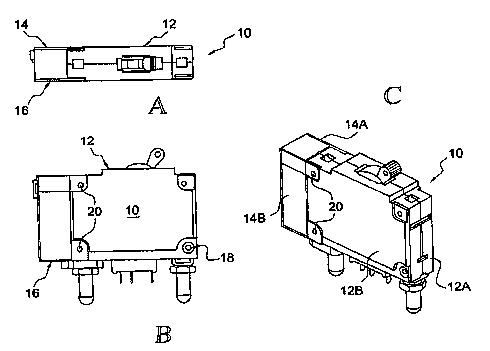
FIGS 1A, 113, and 1C show a standard IEL (magnetic) circuit breaker 10 having
a
generally rectangular case 12 to which the case 14 of a current sensor unit 16
is added
as an attachment. In the form shown, the case of the circuit breaker is
divided along a
central plane and is constituted by two generally rectangular case portions
12A, 12B
joined at the corners by fasteners such as rivets 18, for example. One of the
case
portions serves to hold essential parts of the circuit breaker, while the
other case portion
serves as a cover of the circuit breaker. The case 14 of the current sensor
unit 16 may
be similarly constructed. The case portions 14A, 14B are provided with legs 20
that
overlap respective corners of the circuit breaker case 12 and that are joined
to the
circuit breaker case by the same fasteners 18 that join the portions of the
circuit breaker
case. FIG 8A shows a portion 12A (e.g., half) of a circuit breaker case and a
portion
14A (e.g., half) of a current sensor unit case before attachment of the sensor
unit case
to the circuit breaker case. Other fastening devices (not shown) may be
provided to
assist in joining the portions of the case of the current sensor unit to one
another.
4
CA 02600862 2007-08-16
WO 2007/100316 PCT/US2006/006021
FIG. 2, shows a partially disassembled apparatus of the invention, in which
one
of the portions of the case of the current sensor unit (serving as a cover)
has been
removed to expose parts of the current sensor unit, the details of which will
be
described later. FIG. 3 shows a partially disassembled apparatus of the
invention in
which a portion of each case has been removed to show parts of the
conventional
circuit breaker and parts of the current sensor unit. Since the construction
and
operation of the conventional circuit breaker are well known, only a brief
description will
now be given. _
The circuit breaker comprises a magnetic circuit and an electrical current and
is
essentially a toggle switching mechanism having a handle 22 (or other
operating
mechanism, e.g., rocker) that opens and closes the electrical circuit as the
handle is
moved to an "ON" or "OFF" position. The handle is connected to a contact bar
by a
collapsible link. When the link collapses, it allows contacts of the circuit
breaker to fly
open, thus breaking the electrical circuit. The magnetic circuit may comprise
a frame,
an armature, a delay core and a pole piece. The electrical circuit may
comprise a
terminal, a coil, a contact bar, contacts, and another terminal. As long as
the current
flowing through the circuit breaker remains below 100% of its rated trip
current, the --
breaker will not trip, and the contacts will remain closed. Under these
conditions, the
electrical circuit can be opened and closed by moving the toggle handle. If
the current
is increased beyond the rated current by a predetermined amount, magnetic flux
generated in the coil is sufficient to move the delay core against a spring to
a position
where it comes to rest against the pole piece. This increases the flux in the
magnetic
CA 02600862 2007-08-16
WO 2007/100316 PCT/US2006/006021
circuit, causing the armature to move from its normal position, triggering the
collapsible
link, and opening the contacts.
In accordance with a preferred embodiment of the invention, a main current
carrying conductor 24 is routed through a toroid/Hall Effect device 26 that
may be
mounted on a circuit board 28. The toroid 26A serves as a flux concentrator of
the
magnetic field created by the current. The flux level may be magnified by
passing the
conductor through the toroid multiple times. In this way, very low currents
may be
accommodated. Multiple parallel conductors may be used with,only a portion of
them
passing through the toroid. This method may be used to provide for measurement
of
very high currents.
FIGS. 2 and 3 show the toroid 26A mounted on a circuit board 28 with a main
current conductor 24 routed through the toroid multiple times. See also FIG 6.
FIGS 4
and 5 show (diagrammatically) a single conductor routed through the toroid.
The Hall
Effect device 26B is mounted in a gap in the toroid, as shown in these
figures.
Modification of a standard circuit breaker to incorporate a current sensor
unit in
accordance with the invention is simple. Mechanical modification involves
attachment
of the case of the current sensor unit to an end of the case of the circuit
breaker, and
providing opposed openings in the ends of the respective cases. Electrical
modification
involves re-routing a current-carrying conductor that normally connects a
terminal of the
circuit breaker to the coil of the circuit breaker, so that the conductor
passes through the
toroid (or other suitable magnetic concentrator) along its path from the
terminal to the
coil.
6
CA 02600862 2007-08-16
WO 2007/100316 PCT/US2006/006021
A simplified version of electrical and magnetic components of the invention
will
now be described with reference to FIG 4, which shows six main components of
the
current sensor unit. A description of these components follows:
Hall Effect Device - This component is a programmable Hall Effect device 26B
with capabilities for attaching a programming device (30) to adjust the range,
offset,
temperature compensation, linearity, filtering, and other input and output
parameters of
the sensor.
Magnetic Structure - This component is comprised of a magnetic yoke 26A
(e.g., toroid) incorporating features for inserting and positioning the Hall
Effect device
26B in the magnetic path, directing sufficient magnetic flux to the Hall
Effect device,
attaching the magnetic yoke to the sensor assembly, and electrically and
thermally
insulating the yoke. Versions of the invention intended for high current
applications may
not require the magnetic structure. In this case the Hall Effect device may
simply be
placed in the natural flux path of a current-carrying conductor 24. Other
versions may
use alternative magnetic structures instead of the toroid.
Signal Conditioner - This component (32) can be used to convert the raw
output of the Hall Effect device into a form required by the end user. It can
shift the level
of the Hall Effect device signal and provide gain to increase or decrease the
signal. It is
also capable of providing increased current output. As shown on the schematic
diagram
of Fig. 7, it is represented by the Level Shifter, Primary Gain Stage,
Secondary Gain
Stage (and, optionally, the output stage). This component provides an
enhancement of
the current sensor and is not required for end users that can use the raw
output signal
from the Hall Effect device.
7
CA 02600862 2007-08-16
WO 2007/100316 PCT/US2006/006021
Power Supply - This component (34) is used to convert the power provided by
an end user installation into the regulated voltage and current required by
the circuitry of
the current sensor unit. This component is not required for end user
installations that
provide sufficiently regulated power of the proper voltage and current. It is
an
enhancement that provides value in installations where power is available but
incompatible with the requirements of the other sensor circuitry.
Hall Effect Voltage Regulator - This component (36) provides a stable voltage
to the Hall Effect device so that its output is insensitive to power supply
fluctuations. It
provides enhanced accuracy for applications requiring non-ratiometric
performance.
Ratiometric performance means that the signal from the Hall Effect device will
follow
changes in the input voltage. This behavior is useful in certain applications
and, in this
invention, can be achieved by elimination of the Power Supply and Hall Effect
Voltage
Regulator sections. With these sections gone a percentage increase or decrease
in the
supply voltage to the Hall Effect device will result in an equal percentage
increase or
decrease in the output signal.
Programming Device - This component (30) is not a part of the current sensor
unit but is a tool used to provide calibration and other adjustment functions
on the -
assembly line. Using this tool to set up the current sensor unit reduces the
labor and
inventory required to manufacture the current sensor unit. Individual sensors
can be
adjusted to the required parameters without making changes to the physical
circuitry but
by simply programming the correct values at the time of product assembly.
8
CA 02600862 2007-08-16
WO 2007/100316 PCT/US2006/006021
Following is a more detailed description of the electronic circuitry of an
actual
embodiment organized by functional sections, referring to the schematic
diagram in FIG.
7 and components listed in the accompanying Table 3.
1. Hall Effect Device
The Hall Effect device is used to detect the magnetic field created by a
current
carrying conductor. To better capture the magnetic field and reduce the
effects of spatial
variations a magnetic yoke composed of a magnetically permeable material and
formed
in a shape conducive to concentration of the magnetic field is used. The Hall
Effect
device is inserted into a gap that interrupts the otherwise continuous torus
of magnetic
material. In this way, the magnetic field of any conductor extending through
the center
of the magnetic structure will be induced into the magnetic material. With the
insertion
of the Hall Effect device in the gap, the magnetic circuit can only be
completed by
directing the induced magnetic field through the gap and thus through the
device.
The Hall Effect device is a 3 pin programmable integrated circuit (e.g.,
Micronas
part no. HAL805) containing analog and digital circuitry as well as memory.
Upon
receipt, input signals are converted into digital format. All signal
processing is thereafter performed digitally. After processing, the digital
signal is converted to an analog signal
available at the output. This processing method greatly reduces the effects of
temperature drift, analog offsets, and mechanical stress that result in output
error.
Programming is accomplished by modulating the supply voltage. The device is
designed for use in hostile environmental conditions and has an operating
temperature
range of -40 - 150 C
9
CA 02600862 2007-08-16
WO 2007/100316 PCT/US2006/006021
The programmable options include range, span, output voltage, frequency
response and temperature compensation. Programming for a .5 - 4.5 volt output
range
provides the maximum sensitivity and represents the standard output span used.
Programming tools may include PC based computer applications provided by the
manufacturer of the Hall Effect device and applicable software.
Programming the current range of the sensor is accomplished by connecting the
calibration test equipment to P1 and performing the calibration sequence. In
FIG 2 a
ribbon cable used in programming is shown connected to P1 through a wall of
the case
of the current sensor unit. The calibration software applies minimum and
maximum
current values to the sensor and calculates the parameters necessary to adjust
the Hall
Effect device for the proper output, then loads the correct values into the
Hall Effect
device registers and locks the memory so that it cannot be changed. After
calibration,
the test equipment is disconnected and a program plug is inserted into Pi and
sealed to
prevent removal.
In order to form a magnetic circuit of suitable intensity, it is necessary at
lower
currents to amplify the effective magnetic field by passing the conductor
through the
center of the toroid multiple times, thus increasing the number of ampere-
turns (eg.: 5 -
amperes and 5 passes through the toroid = 25 ampere turns). The minimum
sensitivity
of the Hall Effect device dictates a minimum number of ampere-turns that will
provide
acceptable accuracy.
2. Hall Effect Voltage Regulator
The Hall Effect device exhibits ratiometric behavior. That is, any change in
supply
voltage will be reflected by a proportional change in output level. Obtaining
good
CA 02600862 2007-08-16
WO 2007/100316 PCT/US2006/006021
accuracy therefore depends greatly on the accuracy and stability of the power
supply
serving the Hall Effect device. For this reason the supply used to power the
Hall Effect
device is designed for high accuracy and stability. An LM4050AEM3-5.0
micropower
voltage reference supplies 5.0 volts to a'/a LM124 op amp configured as a Xl
voltage
follower. Both devices exhibit high stability over the full -40 -125 C
temperature range.
Accuracy of this circuit is 0.1 % over the full range.
3. Power Supply
The power supply section comprises a wide input tolerance switching power
supply that provides 12 volt power to the other current sensor circuitry. Any
DC voltage
between 20 and 95 Volts may be used to power the current sensor. The power
supply is
based upon the National Semiconductor LM5008 High Voltage Step Down Switching
Regulator.
4. Level Shifter
The level shifter combines with sections 5, 6, and 7 to form the signal
conditioning circuitry for the current sensor. This section is a Xl voltage
follower that
buffers the voltage set by the divider formed from R6 and R7. The resulting
voltage is
used to provide a non-zero reference for the primary gain stage that will
cause its output
voltage to be shifted. For example, if the minimum voltage out of the Hall
Effect device
is 0.5V and that represents 0 amperes current, then setting the output of the
divider at
0.5V will cause the output of the primary gain stage to be shifted down by 0.5
volts to a
level of zero volts when zero current is applied. R6 and R7 have a resistance
tolerance
of 0.1 % and a temperature coefficient of 25 ppm The output of the level
shifter is
represented by the following formula:
11
CA 02600862 2007-08-16
WO 2007/100316 PCT/US2006/006021
R7
VOUT -5x R6+R7
5. Primary Gain
The primary gain stage is a combination difference and summing amplifier used
to provide amplification of the signal from the Hall Effect device. The series
combinations of R3- R23 and R4- R24 allow precise values of resistance to be
created
from standard resistors. The output voltage is described by the following
formulae:
A) With R29 and R30 u.ninstalled
R1+R3+R23 R4+R24 R3+R23
V u' ~CR2+R4+R24) Rl yRZ Ri VR'
B) With R29 and R30 uninstalled and R1 = R2 and R3 + R23 = R4 + R24
R3+R23
VouI ~~xx - VRI)
q With R1 uninstalled and R29 = R2
R30+R3+R23 R4+R24 R3+R23 VR '
~ u' R2+R4+R24 R30 (~Ra+ V'~29)~ R30
As an example, suppose R29 and R30 are uninstalled, R3 is 249K, R23 is 1 K,
R4 is 249K, R24 is 1 K, RI is 200K, and R2 is 200K. For an input ranging from
.5 to 4.5
volts at R2 and an input (as described previously) of 0.5V at R1, the
amplifier will yield a
range from 0.0 to 5.0 Volts. All resistors must be 0.1 % and 25 ppm in order
to keep
overall error at less than 1%.
6. Secondary Gain Stage
The secondary gain stage is used to buffer the output of the primary gain
stage,
and provide any additional amplification required. As an example, it might be
used to
12
CA 02600862 2007-08-16
WO 2007/100316 PCT/US2006/006021
amplify the 0 - 5 Volt output described previously by 2 times for an output of
0-10 Volts.
For this stage:
R19 + R20
Vour - R19 kl' tn
7. Output Stage
The output stage is an optional feature of the signal conditioning circuitry.
It is
constructed from a complementary Mosfet pair connected in push-pull fashion
and a
suitable biasing resistor network This arrangement provides two advantages
where
needed. First, it is capable of sourcing high currents and second, it is
capable of making
voltage excursions extremely close to the power supply rail.
Operation close to the rail is important for accuracy when signals are small.
Implementing a 0 - 1 volt output requires that the zero value at the output be
less than
milliamps to be within 1% accuracy. For a 0.0 - 100 millivolt output a zero
value of
less than 1 millivolt is required. Operational amplifiers cannot achieve such
performance.
So, even when high output current is not required, it will be necessary to use
the output
stage if operation near zero volts is required.
Electronic Assembly Options
There are several options that are achieved by the inclusion or exclusion of
certain functional sections, and by the installation of correct zero ohm
jumpers. The
production PC board is arranged in such a way that sections may be populated
or left
empty to achieve the desired functionality. Following is a description of the
product
options.
13
CA 02600862 2007-08-16
WO 2007/100316 PCT/US2006/006021
Table 1
Rated Supply Signal High Output
Voltage Conditioning Current
5V Ratiometric
12 Volt 10%
11-30V X
20-95V
20-95V X
20-95V X
Any of the signal conditioned options also have a choice of output voltage
ranges. See
below for examples.
Table 2
Signal R1 R2 R3 R4 R23, R24 ~t6 R7 R19 R2Q R29 1 R30
Conditioned
Oait ut Voltage~ 0-1 300K 200K 49,9K 149.9K 1001 100 1SK 2K None, 0 None None
0 2 0 200K ;249K 249h lI: 1K 1SK 2K None 0 None ~ None
0- 10 200K 200K 249K 249K 1K 1K 18K 2K IOOK 100K None None
1-5 None 200K 200K 200K 0 0 18K 2K .'None 0 200K. 3Q0K
I I
I,
Note: All Resistors are 0.1% 1/16W 25ppm similar to Susumu RR0816I' -,=-B-T5
14
CA 02600862 2007-08-16
WO 2007/100316 PCT/US2006/006021
Table 3
.~ -=
~ >~k kiCkXXXk?C?C?CkkiCXSCkXkSSX~i<kXSCiC kX kk kXSSiSXkk Xk?S
~ Xk kXkXXXk?C?C kDCXkkXkkkX~XXXkX J< kX XiC X XXk
~ AC kkXkXXX X kkSC ~XXX?Sk ~! k iCXX
a e
~ q .tlg
XkXk k k XXk XXXXXO k kDC iG Xkk
c 'E
k k SG DC ?G k ~ ~ .i X X X X
>g o 0
N a vV w
~ y
~~ X k k X k X ~ ~ AC X X k
nn o
~ V5~' y.D Q o j. Q p~ ~ N ~_4 (~ O O p o O M N N 6 N rv ~ z
N N N N t~ t[~,' 2C-+' C
Q~> t~~a '~ ~!9 m Q v w o 0000 00~+l 0
oM o oM o a on~wwwC t7 d ww~~ d
V M a V o~ u~GG~ ~ 'Q~ ~~o e e N N N~~ o0 00 0o w S Q Q Q<~ Q Q N'~ ~ N N rv~~
~ + ~ roE
~O 4y b 8
+ ~i' d c O O~ O O~~~~ O O O O O O~p O O ~ O O O O~D~~ ~' %
0 ~ 0 o w~ ~o w~o .c ~c ~ co ~ o w oo
N~ W tp~V N m v p aN VI w y~ L~ ~+ p p p W W W O O O c~ O a o ~$/~ O O O W 1~
~ tl~
o w w o N u N o~"y ~O a' !r. W' F+ ~+ F F H u u u~a U U U U U Pi U U oF C4 ~ H
U U U p "a o
Q '~ u ~~!~[ ~ ~ ~~y q~ ~ ~ ~ 8pp Spp egp~ 300 8pp 'a ~y{~ ' ',C~ Npp 8pp 8pp
8p0 ~pn ~ 8pp 8yp 8pn ~ ~ 8~p Npp 8a0 8pp ~e p ~ ~ U t
p W Q q ~'"' R r7 R N N W N ~~27 jy N W t0 ttl cV N N "~ ttlN W ctl N e0 af
N 1dd ~~~
w Q o. F i-~ ~ F,'~ w v~ ~ en en rn v> >+ >+ Y~ S~ S~ w w a. >+ ?~ ?~ ~ Ln ~>+
D+ rn m?+ >+ ?~ >+ w w',~ z C~
v~ w w v~ w
n w N v~ n tV v~ n n n n n N y~ n n w v~ v~ v~ w~ n n n a n w w w w w w o~ v~
..rv. . N
Lr ~ r P ~i . +
w o C
R v w w V~ V~ w w w Vl w w w w w w w w V~ w uf w w w w w N w w w w w w w w N w
V~ Vt w w w w w w w N w w A
Vl w 1A N w V1 Y~ V1 Vl V1 V1 Vi w 1n h Vi N h Nl V, V~ Vi h Vl w w Vf Yl Vl w
~t h V~ V1 w w Vl w w Vl Vl V! w Vl ul 41 Vl w W
tl ~ b O O O F. ~a i4 p~~ q~~ fq VI VJ ~ V! VJ O b p O w w vl ~ V
!C y V] V1 FK,1 Vf to LV1 N..N. ~ b ~pp V b~~ ~p~ p~ O O b $ ~ W
9 O O... O O p\ a O q~ y~ H
R R7 e e o g o o W~~ p o PA ~=,~ Vl u LCJJ O
~~ ~ o y o o N o ~ o 0 0 0 0 - o o '~ ~
o M~g~o B~Qg~:axwooooooo. o~ oo= i~~~ ~~ oo O~ ys~
wk wtx~~wk u ~ {'~~7g LSp4aGFGooo Tod7~nO~~ ~E vy~0o00o00~'.LSE oo
O~ O,., N"' R'=': ~ r~d ~ G7 00 ~ iML N N N N 7~ lV Q M~ N M N~G OO C G M OO G
V~i ~~ h O O ~ ~~~ ~
E' m 3
.~ o A Ao 0 0 0 0o 0 0 0.o 'o ~~o, o M H .~0 .~
0 ~ ~ U ~
'~ A A arr M.xix x x a ~r a ~ xi m
c~ x xa x a,a~xxm x y8
[~~y J, 0 0 0 0
; L~ :~ ~7 {~. N ,O ~ ~ Q ~ ~ . N O g N N rv 'v, w N M O ~ O ~ ~ ~ ~ w O O
=fi5
ii TE31010 ~, ~. u c~u c~~ic~'J a a v~'O. a.aaaxn~ ~D ~
CA 02600862 2007-08-16
WO 2007/100316 PCT/US2006/006021
The construction of the case of the current sensor unit can be modified from
that
shown in FIG 8A. FIG 8B shows an embodiment in which portions 14A', 14B' of
the
case of the sensor unit case are hinged to one another.
As stated earlier, one of the advantages of the invention is that a current
sensor
unit can be constructed as an adjunct to a standard circuit breaker with
minimal
modification of the circuit breaker. However, there may be instances in which
it is
desirable to incorporate a current sensor unit of the invention in a case of a
circuit
breaker that has been specifically designed to receive the current sensor
unit. FIG 8C
shows an embodiment in which portions of the current sensor unit case are
integrally
molded with corresponding portions of the circuit breaker case. See, e.g.,
14A", 12A".
FIG 9 shows another embodiment of the invention using a different magnetic
concentrator 26A'. In this embodiment the magnetic concentrator is supported
in a
holder 38 molded as part of one case portion 14A"'of the current sensor. The
magnetic
concentrator is a rectangular annulus and may be comprised of a stack of
laminates
made of Mu metal or ferrite material, for example. A leg of the magnetic
concentrator
26A' extends into a plastic sleeve 40. The leg has opposed parts that meet at
the
center of the sleeve with an insignificant gap. A current carrying conductor
24 from the
circuit breaker is wound around the plastic sleeve. A Hall Effect sensor 26B
is mounted
in a gap in the magnetic concentrator. A circuit board 42 is placed over the
magnetic
structure.
While preferred embodiments of the invention have been shown and described,
changes can be made without departing from the principles and spirit of the
invention,
16
CA 02600862 2007-08-16
WO 2007/100316 PCT/US2006/006021
the scope of which is defined in the claims which follow. For Example, the
sensor unit
can be programmed to measure voltage. AC or DC current or a combination
thereof
can be sensed, for example. Moreover, some of the principles of the invention
can be
used to provide self-contained adjuncts to other types of current-carrying
electrical
devices.
17