Note: Descriptions are shown in the official language in which they were submitted.
CA 02604303 2007-10-05
WO 2006/121559 PCT/US2006/013420
SKYLIGHT SOLAR PANEL ASSEMBLY
CROSS-REFERENCE TO RELATED APPLICATIONS
This application is claims the benefit of U.S. provisional application
Serial No. 60/669,632 filed April 8, 2005.
BACKGROUND OF THE INVENTION
1. Field of the Invention
The present invention relates to plastic molded frames having an
integrated photovoltaic panel.
2. Background Art
The integration of photovoltaic devices into residential and
commercial buildings in an aestlietically pleasing manner is important for the
general
acceptance of such devices. In many convention photovoltaic installations,
solar cell
panels are mounted on brackets fastened to rooftops in a manner that often
contrast
with the appearance of the building. Recently, an appreciation for masking
solar
cells in conventional building components has developed. Typically, such
advanced
materials are referred to as building-integrated photovoltaics ("BIP").
Examples of
components with integrated photovoltaics include curtain walls, awning
systems,
rooftop arrays, skylights, atriums, and the like. Such components, however,
tend
to be expensive to fabricate while presenting complications for easily
replacing
defective or damaged solar cells.
Windows are integral parts of a variety of building components which
include skylights, doors, conventional windows, and the like. Skylights, for
example, have been used to allow light into residential and commercial
buildings
through an opening. The aesthetic value and possible health benefit of having
-1-
CA 02604303 2007-10-05
WO 2006/121559 PCT/US2006/013420
sunlight in buildings have lead to an increasing demand for these structures.
Ideally,
a skylight will let light in while keeping other environmental elements out.
Some
window and skylight assemblies include either colored glass or low-e glass
which
passively enhance the solar control properties of the assemblies. However, few
window assemblies with integrated active components are available. Moreover,
the
assemblies that do exist tend to be complicated and expensive to fabricate.
Skylights have been formed with components made by reaction
injection molding ("RIM"). U.S. Patent Number 5,061,531 ("the '531 patent")
discloses a framed insulating glass unit with an integral skylight frame and
an
integral curb made by the RIM process. In the framed insulating glass unit of
the
'531 patent, two glass plates are molded into a frame member by a polyurethane
RIM process. RIM is a process of molding plastic parts using liquid monomers.
It is capable of forming solid or foam parts that can vary from being flexible
to
extremely rigid. Polyurethanes are probably the most common plastics from
which
parts are made by the RIM process. RIM polyurethane is made by combining an
isocyanate and a polyol.
In the typical RIM process, the liquids are pumped into and combined
in a mixer under a pressure between about 1,500 and 3,000 psi. The liquids are
then
introduced into the mold under a low pressure (about 1 atm). An exothermic
chemical reaction occurs in the mold causing the liquid to solidify without
heating
or cooling. Parts fabricated by RIM offer several advantages over other
molding
processes. Although parts produced by RIM are similar to parts made by
injection
molding, RIM parts may be made with shorter production time and less cost.
Furthermore, RIM does not require high temperatures or pressures typical of
injection molding thereby making it possible to make the molds out of
inexpensive
materials such as aluminum. However, the RIM process presents a number of
considerations that complicate part fabrication. For example, the processing
temperature, pressure and viscosity must be accurately controlled since the
polymerization of the monomers takes place in the mold. Furthermore, the
mixing
head must be completely purged after each part is formed to prevent clogging.
Finally, the relatively protracted cycle times for forming larger parts, and
the
-2-
CA 02604303 2007-10-05
WO 2006/121559 PCT/US2006/013420
limited choices of polymers (mostly pblyurethanes) make RIM a somewhat
undesirable process.
Accordingly, there exists a need for an improved construction
component with integrated photovoltaic devices that are inexpensive to
fabricate and
aesthetically pleasing.
SUMMARY OF THE INVENTION
The present invention overcomes one or more problems of the prior
art by providing in at least one embodiment a framed photovoltaic module
suitable
for integration into a window-containing structure. The framed photovoltaic
module
of this embodiment includes a photovoltaic panel and a plastic frame section.
The
framed photovoltaic module of the present invention is characterized in having
an
outer peripheral edge section about which the plastic frame section is molded.
Accordingly, the plastic frame section encapsulates and/or contacts the outer
peripheral edge section. The framed photovoltaic module of this embodiment is
advantageously integrated into any building component that typically includes
a
window or light-panel. Moreover, the framed photovoltaic module is
advantageously used to mount photovoltaic panels to a building or on a array
designed to hold photovoltaic panels. Such components include, but are not
limited
to, conventional window units, doors, skylights, and the like.
In another embodiment of the invention, methods for making the
framed photovoltaic module set forth above is provided. The method of this
embodiment includes molding by injection molding, vacuum molding, compression
molding, or by RIM.
BRIEF DESCRIPTION OF THE DRAWINGS
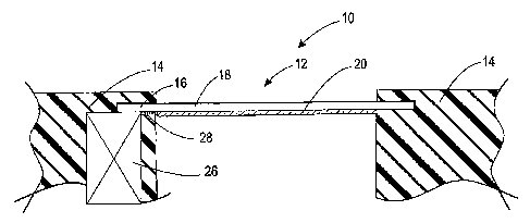
FIGURE 1A is a cross-sectional view of an embodiment of the
invention in which a photovoltaic panel is molded into a plastic frame
section;
-3-
CA 02604303 2007-10-05
WO 2006/121559 PCT/US2006/013420
FIGURE 1B is a cross-sectional view of another embodiment of the
invention in which a photovoltaic panel is molded into a plastic frame
section;
FIGURE 2A is a cross-sectional view of an embodiment of the
invention in which a photovoltaic panel along with a second substrate and
spacer are
molded into a plastic frame section;
FIGURE 2B is a cross-sectional view of another embodiment of the
invention in which a photovoltaic panel along with a second substrate and
spacer are
molded into a plastic frame section;
FIGURE 3A is a cross-sectional view of an embodiment of the
invention in which a photovoltaic panel along with a second substrate are
molded
into a plastic frame section that includes an integral spacer;
FIGURE 3B is a cross-sectional view of another embodiment of the
invention in which a photovoltaic panel along with a second substrate are
molded
into a plastic frame section that includes an integral spacer;
FIGURE 4 is a cross-sectional view of an embodiment of the
invention in which a photovoltaic panel laminated to a second light-panel is
molded
into a plastic frame section;
FIGURE 5A is a cross-section of an embodiment of the invention that
includes a stepped frame section and a spacer;
FIGURE 5B is a cross-section of an embodiment of the invention that
includes a stepped frame section with two substrates laminated together;
FIGURE 5C is a cross-section of an embodiment of the invention that
includes a stepped frame section and a spacer with a solar cell attached to
the second
substrate;
-4-
CA 02604303 2007-10-05
WO 2006/121559 PCT/US2006/013420
FIGURE 6 is a schematic of a multi-layer solar cell that is used in one
embodiment of the present invention; and
FIGURE 7 is a perspective view of an embodiment of the present
invention with a plastic frame and a curb adapted to be placed on a rooftop.
DETAILED DESCRIPTION OF THE PREFERRED,EMBODIMENTS
Reference will now be made in detail to presently preferred
compositions or embodiments and methods of the invention, which constitute the
best modes of practicing the invention presently known to the inventors.
As used herein, the term "light-panel" means a medium through
which light is admitted. Such media include transparent or translucent glass
and
plastic panels.
As used herein, the term "photovoltaic panel" means a structure or
assembly that includes at least one solar cell.
As used herein, the term "transmittance" means the percentage of
incident visible light that is transmitted through an object. Formally, this
is the
amount of incident light (expressed as a percent) minus that amount reflected
and
absorbed.
In an embodiment of the present invention, a framed photovoltaic
module is provided. The framed photovoltaic module of this embodiment includes
a photovoltaic panel and a plastic frame section encapsulating and/or
contacting an
outer peripheral edge section of the photovoltaic panel. In at least one
aspect of this
embodiment, the window and skylight frames disclosed in U.S. Patent
Application
No. 10/639,410 filed on August 12, 2003, and U.S. Patent Application No.
11/057,391 filed on February 12, 2005 are used for the plastic frame sections
in the
present invention. The entire disclosures of each of these applications are
hereby
-5-
CA 02604303 2007-10-05
WO 2006/121559 PCT/US2006/013420
incorporated by reference. Specifically, the frame sections and curb sections
of
these applications are used in one embodiment of the present invention with a
photovoltaic panel replacing at least one light panel or window.
With reference to Figures 1A, 1B, 2A, 2B, 3A, and 3B, cross-
sectional views of various framed photovoltaic modules embraced by the present
invention are provided. With reference to Figure 1A, framed photovoltaic
module
includes photovoltaic panel 12 and plastic frame section 14. Plastic frame
section 14 is molded to a portion of outer peripheral edge section 16 of
photovoltaic
panel 12. Photovoltaic panel 12 includes one or more solar cells. Virtually
any
10 solar cell design may be used in the practice of the invention. For
example,
crystalline silicon, polycrystalline silicon, amorphous silicon, copper indium
diselenide, CdZnS/CuInGaSe2, ZnCdS/CdTe, and gallium indium phosphide on
gallium arsenide solar cells may be used. Moreover, thin film solar cells are
particularly useful in the practice of the invention. In a variation of this
embodiment, photovoltaic panel 12 includes substrate 18 with one or more solar
cells 20 attached thereto. In a refinement, one or more solar cells 20 are
attached to
substrate 20 with an adhesive. In another refinement, one or more solar cells
20 are
attached to substrate 20 with an adhesive. In still another refinement, one or
more
solar cells 20 are attached to substrate 20 by molding the solar cells into
the
substrate. Solar cells 20 may or may not extend to the outer edge of substrate
18
in this variation. In the variation of Figure 1A, light must pass through
substrate
18 before reaching one or more solar cells 20. Therefore, substrate 18 is
typically
first light-panel with high light transmission properties. Typically, the
first light-
panel transmits at least 50 percent of incident visible light. In most
applications, the
first light panel transmits greater than about 75 percent of incident visible
light.
Also schematically illustrated in Figure 1A is the inclusion of electrical
connector
26 within plastic frame section 14 which is in electrical contact with grid
28.
Electrical connector 26 allows collection of the electricity generated by
photovoltaic
panel 12. Electrical connector 26 may be molded in place when plastic frame
section 14 is molded. Figure 1B provides a variation in which light is able to
reach
one or more solar cells 20 without passing through substrate 18. In this
variation,
one or more solar cells 20 are overcoated with a transparent protective layer.
In this
-6-
CA 02604303 2007-10-05
WO 2006/121559 PCT/US2006/013420
variation, substrate 18 can be either opaque or transparent. In window or
skylight
applications, portions of substrate 18 may not be covered with solar cells. In
such
refinements, substrate 18 is advantageously transparent in order to allow
light to
enter into a building.
With reference to Figures 2A and 2B, variations of a framed
photovoltaic module having two substrates are provided. Figure 2A illustrates
an
embodiment in which framed photovoltaic module 10 further includes second
substrate 22 with spacer 24 positioned between photovoltaic panel 12 and
second
substrate 22. In this variation, one or more solar cells are attached to
substrate 18
as set forth in connection to the description of Figure 1A. In a refinement of
this
variation, second substrate 22 is a light-panel that transmits visible light.
Figure
2B, provides a variation in which one or more solar cells 20 are attached to
second
substrate 22. In this variation, substrate 18 is again transparent (i. e. , a
light panel)
while second substrate 22 can be either opaque or transparent (i.e., a second
ligllt
panel). In window or skylight applications, portions of second substrate 22
may not
be covered with solar cells. In such refinements, second substrate 22 is
advantageously transparent in order to allow light to enter into a building.
With reference to Figures 3A and 3B, variations of a framed
photovoltaic module with a spacer section integral to and continuous with a
plastic
frame section are provided. In such variations framed photovoltaic module 10
includes a spacer section 30 that is integral to the plastic frame section 14.
Figure
3A provides a variation in which one or more solar cells 20 are attached to
substrate
18. The details of this attachment and the properties of substrate 18 are the
same
as that set forth above in connection with the description of Figures 1A and
2A.
Figure 3B provides a variation in which one or more solar cells 20 are
attached to
second substrate 22. The details of this attachment and the properties of
second
substrate 22 are the same as that set forth above in connection with the
description
of Figure 2B.
With reference to Figure 4, an embodiment of the invention in which
a solar panel is laminated to a second substrate is provided. In this
embodiment,
-7-
CA 02604303 2007-10-05
WO 2006/121559 PCT/US2006/013420
framed photovoltaic module 10 includes photovoltaic panel 12 and plastic frame
section 14. As set forth above, plastic frame section 14 is molded to a
portion of
outer peripheral edge section 16 of solar panel 12. Photovoltaic panel 12
includes
substrate 18 with one or more solar cells 20 attached thereto. Second
substrate 22
is laminated to photovoltaic panel 12 by lamination layer 40. Lamination layer
40
is formed from any type of lamination material that does not appreciably
degrade the
performance of solar cells 20. Second substrate 22 can be either opaque or
transparent (i.e., a light panel) as set forth above in connection with the
description
of Figure 2A. When solar cells 20 are thin film solar cells, ethylene vinyl
acetate
("EVA") is an example of a laminate that can be used to laminate photovoltaic
panel
12 to substrate 22.
With reference to Figures 5A, 5B and 5C, a cross-section of an
embodiment of the invention that includes a stepped frame section is provided.
U.S.
Patent Application No. 10/639,410 filed on August 12, 2003 and U.S. Patent
Application No. 11/057,891 filed on February 12, 2005 discloses the
utilization of
using a step frame section in window applications which is extended by one or
more
embodiments of the present invention. In this embodiment, framed photovoltaic
module 70 includes photovoltaic panel 72 and stepped frame section 74 (i. e. ,
the
plastic frame section). Photovoltaic pane172 includes substrate 76 and one or
more
solar cells 78. As set forth above, substrate 76 is typically a first light-
panel.
Stepped frame section 74 includes lower step surface 80 and upper step surface
82.
Optionally, stepped frame section 74 covers outer peripheral section 84 of
photovoltaic module 70 with cover 86. Cover 86 is also integral to stepped
frame
section 74. Moreover, in some variations peripheral section 84 does not
contain
any solar cells. Framed photovoltaic module 70 also includes second substrate
88.
Second substrate 88 can be either opaque or transparent (i.e., a second light
panel).
In window or skylight applications, portions of second substrate 88 may not be
covered with solar cells. In such refinements, second substrate 22 is
advantageously
a light panel and transparent in order to allow light to enter into a
building.
Still referring to Figure 5A, first substrate 76 has a first length and
a first width and second substrate 88 has a second length and a second width
such
-8-
CA 02604303 2007-10-05
WO 2006/121559 PCT/US2006/013420
that when photovoltaic pane172 and second transparent panel are attached to
stepped
frame section 74, stepped frame section 74 has an edge detail complementary to
the
combined edge detail of photovoltaic panel and the second transparent
substrate (and
a spacer if present). Specifically, lower step surface 80 opposes a peripheral
section
of second substrate 88 and upper step surface 82 opposes either spacer 90 or a
peripheral section of photovoltaic panel 72, or a portion of both spacer 90
and
photovoltaic panel 72. Moreover, the first length is greater than the second
length
and the first width is greater than the second width.
With reference to Figure 5B, a variation in which second substrate
88 and photovoltaic panel 72 are laminated together is provided. In this
variation,
laminate 92 is used to laminate photovoltaic panel 72 and second substrate 88
together. The lamination details are the same as those set forth above in
connection
witli the description of Figure 4.
With reference to Figure 5C, a variation in which one or more solar
cells 78 are attached to second substrate 88 is provided. The detail of this
attachment are the same as those set forth above in connection with the
description
of Figure 2B.
Figures 5A and 5B also provide a demonstration of the modular
features of an embodiment of the invention which is important for the
relatively easy
and inexpensive replacement of damaged or defective solar cells. Photovoltaic
frame 94 includes stepped frame section 74 with photovoltaic pane172 and
second
light-panel 88 molded tlierein. Photovoltaic frame 94 is adapted to be placed
against
curb section 96 which may be placed on a roof, window or door. Drip drain 98
is
optionally included in applications such as a skylight in which condensation
may
occur.
In Figures lthrough 5, the photovoltaic panel is such in some
variations that the solar cell is positioned on an interior surface of a
substrate.
Specifically, light passes through the substrate before impinging on the solar
cell.
In should be appreciated that configurations in which the solar cell is
positioned on
-9-
CA 02604303 2007-10-05
WO 2006/121559 PCT/US2006/013420
an exterior substrate surface are also embraced by the present invention. For
example, light will impinge on the solar cell before proceeding through the
substrate. Accordingly, the following arrangements are included in the
invention -
solar cell attached to a first substrate contacting the plastic frame section
of the
invention; solar cell attached to a first substrate and a second substrate
(with or
without a spacer and with or without lamination as set forth above) contacting
the
plastic frame sections set forth above.
In an important variation of the present invention, the framed
photovoltaic modules set forth above comprises one or more sections that are
transparent. U.S. Pat. Nos. 4,663,495 and 6,180,871 disclose examples of
transparent solar cells that are useful in the present invention. The entire
disclosure
of these patents are hereby incorporated by reference. In one variation, this
transparency is achieved by providing sections of the photovoltaic module
without
any solar cell attached. In other variations, the one or more sections that
are
transparent have a transmittance of at least 1 % (sum if more than one). In
still other
variations, the one or more sections that are transparent have a transmittance
of at
least 5 % (sum if more than one). In still other variations, the one or more
sections
that are transparent have a transmittance of at most 20% (sum if more than
one). In
yet other variations, the one or more sections that are transparent have a
transmittance of at most 15 % (sum if more than one). Multi-film solar cells
are
particularly useful in achieving such transmittances when made sufficiently
thin to
allow some transmission of visible light. Figure 6 provides a schematic cross-
section of a multi-film solar cell that is used in an embodiment of the
invention.
Solar cell 100 includes first transparent substrate 102 over which first
electrically
conductive layer 104 is disposed. First doped silicon layer 106 is in turn
disposed
over at least a portion of first electrically conductive layer 104. Second
doped
silicon layer 108 is disposed over first doped silicon layer 106. Finally,
second
electrically conductive layer 110 disposed over second doped silicon layer
108. The
first doped photovoltaic layer 106 and second doped photovoltaic layer 108
each
individually comprise a component selected from the group consisting of
crystalline
silicon, amorphous silicon, and polycrystalline. Moreover, first doped
photovoltaic
layer 106 and second doped photovoltaic layer 108 each individually include an
-10-
CA 02604303 2007-10-05
WO 2006/121559 PCT/US2006/013420
impurity selected from the group consisting of a p + type impurity, a p type
impurity, and an n type impurity. However, first doped photovoltaic layer 106
and
second doped photovoltaic layer 108 must be doped in such a manner as to form
a
photovoltaically active junction. Typically, if first doped photovoltaic layer
106 is
p type or p + type, then second doped photovoltaic layer 108 is n type.
Similarly,
if first doped photovoltaic layer 106 is n type , then second doped
photovoltaic layer
108 is p type or p+ type. Solar cell 100 includes first conductive layer 102
and
second conductive layer 110. Examples of materials that can be used to form
first
electrically conductive layer 102 and second electrically conductive layer 110
are
transparent electrical conductors which include indium tin oxide ("ITO"),
doped tin
oxide, doped zinc oxide, and combinations tliereof. Moreover; when such
transparent electrical conductors are employed, a set of metal grids attached
thereto
may optionally be used to assist in the collection of electricity. In some
variations,
metal grids may be substituted for the transparent electrical conductors.
With reference to Figure 7, an embodiment of the present invention
in which the framed photovoltaic module of the invention is incorporated into
a
window -containing component such as a skylight is provided. Window assembly
150 includes photovoltaic frame 152 and curb 154. Photovoltaic frame 152
includes
photovoltaic panel 156. Moreover, photovoltaic frame 152 includes the plastic
frame section as set forth above. Similarly, the details of photovoltaic panel
156 are
also the same as those set forth above. Curb 154 includes flange region 158
which
may be placed on a rooftop and sealed in a manner known to those skilled in
the art
of skylight installation. Flange region 158 optionally includes holes 160 to
allow
fastening to a roof or other structure. In another variation of this
embodiment, curb
154 and photovoltaic frame 152 are not separate pieces and are instead a
single
piece. It should also be appreciated that a series of wires used to collect
electricity
from photovoltaic panel 156 are in one variation positioned in one or more
cliannels
molded into the photovoltaic frame 152 and curb 154. In other variations, such
wires are placed in the corners of the window assembly.
The frame photovoltaic modules set forth above are made by a variety
of molding processes. For example, the photovoltaic modules of Figures 1-5 and
-11-
CA 02604303 2007-10-05
WO 2006/121559 PCT/US2006/013420
7 may be formed by injection molding, vacuum molding, compression molding, or
by RIM. When the RTM process is used to form the photovoltaic modules of the
invention, preferably, polyurethane is used as the material of construction.
In such
a process, an isocyanate component is reacted with an isocyanate-reactive
component (i. e. , a polyol) in a mold having an interior cavity complementary
to the
framed photovoltaic module. In the typical polyurethane producing process that
is
useful in the practice of the invention, an isocyanate and a polyol are
reacted
together. Isocyanate usable in the present invention include both
multifunctinal
aromatic isocyanate and multifuntional aliphatic isocyanates. Multfunctional
isocyanates include diisocyanates, triisocyanates, and the like. Examples of
useful
isocyanates include, but are not liunited to, toluene diisocyanate ("TDI"),
methylene-4,4'-diphenyl diisocyanate ("MDI"), and a polymeric isocyanate
("PMDI"). Examples of polyols include, but are not limited to, polyethylene
glycols and polyester polyols. Specific diols usable in the invention include,
but are
not limited to, ethylene glycol, diethylene glycol, 1,4-butanediol, 1,6-
hexanediol,
and the like. Also usable as the polyol are alcohol-terminated polyethers such
as
polyethylene oxide and polypropylene oxide and alcohol-terminated polyesters
such
as poly-1,4-butylene adipate. Usually, the reaction between the polyol and the
isocyanate is carried out in the presence of catalysts. Various additives can
be used
to improve the fire performance, chemical stability, and the like.
Polyurethanes
made with aliphatic isocyanates are somewhat more useful due to the tendency
of
aromatic diisocyanates to yellow with exposure to light.
A particularly useful polyurethane composition and RIM molding
process is provided by U.S. Pat. No. 6,242,555 (the '555 patent), the entire
disclosure of which is hereby incorporated by reference. Specifically, in
accordance
with this process an isocyanate component containing an isophorone
diisocyanate
(IPDI) trimer/monomer mixture having an NCO content of from 24.5 to 34 % by
weight, is reacted with isocyanate-reactive components in the presence of at
least
one catalyst component, at least one pigment component, and at least one
antioxidant/UV absorber component. The isocyanate-reactive components comprise
a polyetherpolyol having terminal OH groups, an average nominal functionality
of
2 to 4, and an average equivalent weight of from 800 to 4000; at least one
chain
-12-
CA 02604303 2007-10-05
WO 2006/121559 PCT/US2006/013420
extender component having as functional groups only aliphatic or alicyclic OH
groups; and at least one amine-initiator component. The catalyst component is
selected from the group consisting of organolead (II), organobismuth (III),
and
organotin (IV) catalysts.
The preferred molding process is chosen to improve strength and to
minimize part weight and to provide optimum thermal insulation qualities. To
this
end, framed photovoltaic modules optionally include one or more hollow cores
that
may be filled with a foamed plastic. Framed photovoltaic modules with hollow
cavities may be made by gas assisted injection molding which uses a
conventional
injection molding press equipped with a spillover control and a mold equipped
with
gas injection and spillover points. Suitable gas assisted injection molding
processes
which may be used to form the skylight frame-curb assembly of the present
invention are described in U.S. Patent No. 6,019,918. The entire disclosure of
this
patent is hereby incorporated by reference. The foam material is then
introduced
through inlet holes after the frame is molded. Alternatively, the part can be
molded
utilizing a plastic foaming agent, the surface of the plastic part having a
smooth
uniform skin while the inner core contains a series of gas bubbles forming a
rigid
foam or sponge-like core. The skylight frame-curb assembly may also be made by
compression molding using either sheet molding compound ("SMC") or bulk
molding compound.
As set forth above, the RIM process is particularly useful in forming
the framed photovoltaic modules of the invention. In such a process, an
isocyanate
component is typically reacted with an isocyanate-reactive component (i. e. ,
a polyol)
in a mold having an interior cavity with a region complementary to the framed
photovoltaic modules. A particularly useful polyurethane composition and RIM
molding process is provided by U.S. Pat. No. 6,242,555. The details of this
process are set forth above and in this patent. Moreover, the application of
one or
more coupling agents prior to molding is found to further enhance adhesion
when
glass panels are used as part of the photovoltaic panel and the second light-
panel.
More preferably, two or more coupling agents are applied to the glass surfaces
prior
to molding of a construction incorporating the frame sections. The details of
the
-13- .
CA 02604303 2007-10-05
WO 2006/121559 PCT/US2006/013420
coupling agents is the same as that set forth above. In a variation the glass
panels
are treated with one or more primers. Useful primers include one or more of
the
following components: organosilanes, polyurethanes, polyesters, pigments, and
solvents. Examples of suitable primers include Betaseal' 43518 Glass Primer
and
Betaseal' 43520A Glass Primer commercially available from Dow Chemical
Company. Betaseal' 43518 Glass Primer is a proprietary composition which
includes toluene, methyl alcohol, and an organosilane. Betaseall 43520A Glass
Primer is a proprietary composition which includes toluene, methyl ethyl
ketone,
carbon black, n-butyl acetate, potassium oxide, xylene, polyurethane,
polyester, and
an organosilane. Typically, the glass is first treated with BetasealTM 43518
Glass
Primer and then Betaseal' 43520A. It is readily apparent that these primers
and in
particular the Betaseal' 43518 Glass Primer and Betaseall 43520A contain a
number of components that improve adhesion of the RIM molded frame to the
glass
panels.
While embodiments of the invention have been illustrated and
described, it is not intended that these embodiments illustrate and describe
all
possible forms of the invention. Rather, the words used in the specification
are
words of description rather than limitation, and it is understood that various
changes
may be made without departing from the spirit and scope of the invention.
-14-