Note: Descriptions are shown in the official language in which they were submitted.
CA 02605209 2007-10-16
1
DESCRIPTION
METAL BASE CIRCUIT BOARD, LIGHT-EMITTING DIODE AND LED
LIGHT SOURCE UNIT
TECHNICAL FIELD
The present invention relates to a metal base
circuit board which can be bent with excellent
electromagnetic wave-shielding performance while securing
heat dissipation performance and electrical insulating
performance, and a light-emitting diode (LED) and LED
light source unit employing it. Particularly, it relates
to a LED light source unit suitable for a backlight of a
liquid crystal display device.
BACKGROUND ART
In recent years, circuit boards for mounting
semiconductors are required to have the boards small-
sized and to accomplish high density mounting and high
performance. Further, it has been a problem how to
dissipate the heat generated from e.g. semiconductor
elements in a narrow space limited by small-sizing or
high power of e.g. the semiconductor elements.
Particularly, a metal base circuit board having a circuit
formed by bonding a metal foil via an insulating layer on
a metal plate has been commonly employed for the reason
that it is excellent in heat dissipation performance
CA 02605209 2007-10-16
2
mainly in the electric power source field or the
automobile electric installation field.
However, in a metal base circuit board, the
thickness of the base board is usually from 1.0 mm to 3.0
mm, whereby it is difficult to reduce the thickness, and
the installation site is rather limited. Further, it has
a structure formed via a thin insulating layer on a metal
plate, whereby there has been a problem such that noises
are likely to occur, or malfunction of a module is likely
lo to occur.
In order to shield noises or to increase the heat
dissipation performance, a metal base multilayer board is,
for example, known wherein an upper layer circuit board
having a circuit is laminated, via an adhesive agent, on
the entire surface or a part of the surface of a metal
base circuit board (Patent Document 1).
In such a construction, an adhesive layer poor in
the heat conductivity is present between the metal plate
and the upper layer board, and in a case where a high
power element is mounted on the upper layer circuit
pattern, the heat dissipation performance tends to be
inadequate, and the temperature of the element tends to
rise, thus leading to a problem of malfunction.
In order to solve such a problem of heat dissipation
performance, a metal base circuit board having a highly
heat conductive insulating layer is known (Patent
Document 2).
CA 02605209 2007-10-16
3
However, the metal plate was thick and could not be
installed as attached along the shape of a case such as a
case having a curved surface, and thus the heat
dissipation performance of the insulating layer could not
s be sufficiently utilized. Besides, a large space was
required for its installation, since it could not be
installed in a bent form, and there was a problem such
that the module could not be small-sized.
On the other hand, a metal base circuit board having
lo an insulating layer made of e.g. an epoxy resin
containing an inorganic filler formed on a metal plate,
and having a circuit pattern formed thereon, is excellent
in heat dissipation performance and electrical insulating
performance and thus is used as a circuit board for an
is electronic equipment for e.g. automobiles and
communication instruments having highly heat generating
electronic components mounted (Patent Document 3).
If a metal base circuit board can be optionally bent,
the limitation in the installation site which used to be
20 limited to installation on a flat portion, will be
relaxed, and it will be possible to adhere, bond or
closely attach by e.g. a screw it to a side or bottom
surface or to a stepped or curved surface of a case,
whereby an electronic equipment having a highly heat
25 generating electronic component mounted, can be small-
sized. Further, if a metal base circuit board itself can
be made thin, it can be inserted or fixed in a narrow
CA 02605209 2007-10-16
4
space, whereby an electronic equipment having a highly
heat generating electronic component mounted, can be made
thin.
It has been proposed that by a method of heating a
s metal base circuit board at a high temperature of at
least 120 C, i.e. by carrying out bending or drawing in
such a state that the metal base circuit board is heated
at a temperature higher by at least 10 C than the glass
transition temperature (Tg) of the insulating layer, the
lo metal base circuit board having a non-flat portion is
used also as a case or an electronic circuit package
(Patent Document 4).
Further, a light-emitting diode (LED) light source
unit using a light-emitting diode (LED) as a light source,
15 has been used in various fields, but, for example, in a
light source for backlight of a liquid crystal display
device, it has been common to use a small size
fluorescent tube so-called CFL (compact fluorescent lamp).
The light source of the above CFL (compact
20 fluorescent lamp) adopts a construction such that Hg
(mercury) is sealed in a discharge tube, and ultraviolet
rays discharged from mercury excited by electrical
discharge will impinge on the phosphor on the tube wall
of CFL (compact fluorescent lamp) and will be converted
25 to visible light. Therefore, recently, from the
viewpoint of the environment protection, it has been
desired to use a substitute light source not using
CA 02605209 2007-10-16
hazardous mercury.
As a new light source, one using a light-emitting
diode (hereinafter referred to simply as "LED") has been
proposed. With LED, the light has directional
5 characteristics, and particularly with a surface mounting
type on e.g. a flexible board, the light will be taken
out in one direction, and as different from a structure
using conventional CFL (compact fluorescent lamp), the
light loss is small, and thus, it is used as a light
lo source for backlight in a planar light source system
(Patent Document 5).
The backlight using LED as a light source is now
being widely used as backlight of a liquid crystal
display device along with reduction of the price,
ls improvement in the luminous efficiency and environmental
regulations. At the same time, along with the higher
brightness of a liquid crystal display device and
enlargement of the display area, the increase in number
of LED mounted on e.g. a flexible board and the trend for
20 higher output are in progress in order to improve the
luminescence.
However, the light source of LED has low luminance
efficiency, and majority of the input power to illuminate
LED will be discharged as heat. When an electric current
25 is conducted, LED generates heat and becomes to have a
high temperature due to the generated heat, and in an
extreme case, LED will be destroyed. Also in a backlight
CA 02605209 2007-10-16
6
using LED as a power source, such generated heat will be
accumulated in LED and the board having LED mounted, and
along with the increase of the temperature of LED, the
luminance efficiency of LED itself tends to deteriorate.
Besides, if it is attempted to increase the number of LED
to be mounted or to increase the input power in order to
make the backlight bright, the heat generation will
further increase, and it is therefore important to remove
such heat.
lo In order to reduce the heat accumulation in the LED-
mounted board and to reduce the temperature rise of a LED
chip, it has been proposed that a metal film having a LED
chip mounted on a LED chip-mounted surface of a LED-
mounted board, a metal drive wiring to supply a drive
current to the LED chip and a metal film pattern intended
for heat dissipation, are formed, a metal film for heat
dissipation is formed on a surface facing the LED chip-
mounted surface, and a metal through-hole is formed in a
thickness direction of the LED chip-mounted board to
connect the metal pattern on one main surface side to the
metal film for heat dissipation on the other main surface
side, so that heat generation from LED is dissipated
through the metal through-hole to the rear side metal
film (Patent Document 6).
However, in a case where the shape of LED to be
mounted is small, the area of the mounted metal film will
be limited, and the number of metal through-holes which
CA 02605209 2007-10-16
7
can be formed immediately beneath LED will be limited,
and in a case where a metal film pattern can not be
formed on the mounted board from the restriction of the
board area, there will be a problem such that the heat
s generated by LED can not efficiently be released to the
rear side of the board.
Further, if a metal base circuit board using a metal
base plate having a thickness of 2 mm is used instead of
the flexible board, good heat dissipation can be obtained
lo without necessity to provide metal through-holes, but
there will be a problem that the thickness of the board
tends to be thick, and it will be necessary to enlarge
the size for punching out from e.g. an electrode and a
circuit pattern over the flexible board, whereby the
15 board area is obliged to be large. Further, it is not
possible to optionally bend a portion other than the LED-
mounted portion, whereby e.g. the position to form an
input terminal will be restricted.
Besides, if the thickness of the metal base of the
20 metal base circuit board is made thin to have such a
structure that the size for punching out from e.g. an
electrode and a circuit pattern is made small like a
flexible board, even when the metal base circuit board is
slightly bent, the insulating layer will have cracking
25 and become useless. Likewise, there has been a problem
that the LED-mounted portion can not be optionally bent.
Further, a metal base circuit board using a metal
CA 02605209 2007-10-16
8
foil of from about 9 to 40 lam having a conductive circuit
provided via an insulating layer containing a heat
conductive filler and having heat dissipation performance
and good bendability at room temperature, instead of a
s conventional polyimide type insulating layer, has been
developed, since it can be used as being bent at room
temperature and has bending processability.
However, if the conductive circuit was bent at an
angle of 90 with a very small radius of curvature of at
lo most 0.5 mm, the insulating layer at the bent portion was
likely to have cracking and become useless. Therefore,
if it was reinforced with a coverlay having an epoxy
adhesive layer formed on a polyimide film, it was
possible to prevent cracking in the insulating layer at
is the bent portion, but the bendability decreased, and
there was a problem that it became difficult to bend it
at an angle of at least 90 with a very small radius of
curvature of at most 0.5 mm.
Further, in a case where a circuit board for
20 mounting a semiconductor or a small size precision motor
is, for example, mounted, there has been a problem that
noises are likely to occur, or malfunction of a module is
likely to occur.
Patent Document 1: JP-A-05-037169
25 Patent Document 2: JP-A-09-139580
Patent Document 3: JP-A-62-271442
Patent Document 4: JP-A-2001-160664
CA 02605209 2013-01-25
71416-378
9
Patent Document 5: JP-A-2005-293925
Patent Document 6: JP-A-2005-283852
DISCLOSURE OF THE INVENTION
s OBJECT TO BE ACCOMPLISHED BY THE INVENTION
Some embodiments of the present invention
provide a metal base circuit
board which has good heat dissipation performance and
good bendability and is excellent also in electromagnetic
shielding performance and electrical insulating
performance; a process for its production; and a hybrid
integrated circuit, an LED module reinforced by a
coverlay, and a bright long-life LED light source unit
where damage of LED is prevented.
MEANS TO ACCOMPLISH THE OBJECT
Namely, some embodiments of the present invention
provide the following:
(1) A metal base circuit board having an insulating
layer and a conductive circuit or metal foil alternately
laminated, characterized in that the thickness of the
conductive circuit or metal foil is from 5 pm to 450 pm,
the insulating layer is made of a cured product of a
resin composition comprising an inorganic filler and a
thermosetting resin, and the thickness of the insulating
layer is from,9 pm to 300 pm.
CA 02605209 2007-10-16
(2) The metal base circuit board according to the above
(1), wherein at least one through-hole to be used for
electrically connecting conductive circuits or metal
foils, is at least 0.0078 mm2.
5 (3) The metal base circuit board according to the above
(1) or (2), wherein the thermal conductivity of the
insulating layer is from 1 to 4 W/mK.
(4) The metal base circuit board according to any one of
the above (1) to (3), wherein the glass transition
lo temperature of the insulating layer is from 0 to 40 C.
(5) The metal base circuit board according to any one of
the above (1) to (4), wherein the insulating layer is a
cured product of a resin composition comprising from 25
to 60 vol% of a thermosetting resin and the rest being an
inorganic filler having a sodium ion concentration of at
most 500 ppm and comprising spherical coarse particles
having the maximum particle size of at most 75 um and an
average particle size of from 5 to 40 um and spherical
fine particles having an average particle size of from
0.3 to 3.0 um.
(6) The metal base circuit board according to any one of
the above (1) to (5), wherein the thermosetting resin
comprises a hydrogenated bisphenol F and/or A epoxy resin.
(7) The metal base circuit board according to the above
(6), wherein the thermosetting resin comprises a
straight-chain epoxy resin having an epoxy equivalent of
from 800 to 4,000.
CA 02605209 2007-10-16
11
(8) The metal base circuit board according to the above
(6) or (7), wherein the thermosetting resin contains a
polyoxyalkylene polyamine as a curing agent.
(9) The metal base circuit board according to any one of
s the above (6) to (8), wherein the chloride ion
concentration in the thermosetting resin is at most 500
ppm.
(10) The metal base circuit board according to any one of
the above (1) to (9), wherein when the circuit board is
lo bent at an optional portion at an angle of at least 900
with a radius of curvature of from 1 to 5 mm, the
withstand voltage between conductive circuits or metal
foils is at least 1.0 kV.
(11) The metal base circuit board according to any one of
ls the above (1) to (10), wherein a conductive circuit is
formed on a metal foil via an insulating layer, and a
coverlay having a thickness of from 5 pm to 25 pm is
further formed, and wherein at least a part of the
coverlay is removed to form a slit at a portion where the
20 conductive circuit is not formed.
(12) The metal base circuit board according to the above
(11), wherein the slit is formed to have a length
corresponding to from 50% to 95% of the length of the
portion to be bent.
25 (13) The metal base circuit board according to the above
(11) or (12), wherein the thickness of the coverlay is
from 5 pm to 25 pm.
CA 02605209 2009-08-17
71416-378
12
(14) The metal base circuit board according to any one of
the above (11) to (13), which is bent along the slit.
(15) The metal base circuit board according to any one of
the above (11) to (14), wherein the insulating layer
surface is bent at an angle of at least 900 with a radius
of curvature of from 0.1 to 0.5 mm.
(16) The metal base circuit board according to any one of
the above (11) to (15), wherein a layer having a magnetic
loss or a layer having a dielectric loss is laminated on
lo the surface of the coverlay.
(17) The metal base circuit board according to any one of
the above (11) to (16), wherein the layer having a
magnetic loss comprises a magnetic material having an
aspect ratio of at least 2, and an organic binder, the
content of the magnetic material is from 30 to 70 vol%,
and the thickness of the layer having a magnetic loss is
from 3 pm to 50 pm.
(18) The metal base circuit board according to any one of
the above (11) to (16), wherein the layer having a
dielectric loss comprises a carbon powder having a
2
specific surface area of from 20 to 110 m/g, and an
'organic binder, the content of the carbon powder is from.
5 to 60 vol%, and the thickness of the layer having a
dielectric loss is from 3 pm to 50 pm.
(19) A hybrid integrated circuit using the metal base
circuit board as defined in any one of the above (1) to
(10).
CA 02605209 2007-10-16
13
(20) A light-emitting diode having at least one light-
emitting diode electrically connected to the conductive
circuit of the metal base circuit board as defined in any
one of the above (11) to (18).
(21) A LED light source unit having the metal base
circuit board as defined in any one of the above (1) to
(18) disposed on a surface of a case via an adhesive tape
and having at least one light-emitting diode (LED)
mounted on the conductive circuit of the metal base
io circuit board.
(22) The LED light source unit according to the above
(21), wherein the adhesive tape has a thermal
conductivity of from 1 to 2 W/mK and a thickness of from
50 pm to 150 pm.
(23) The LED light source unit according to the above
(21) or (22) wherein the adhesive tape comprises a
polymer comprising acrylic acid and/or methacrylic acid.
(24) The LED light source unit according to any one of
the above (21) to (23), wherein the adhesive tape
contains a heat-conductive electrically insulating agent
in an amount of from 40 to 80 vol%.
(25) The LED light source unit according to any one of
the above (21) to (24), wherein the heat-conductive
electrically insulating agent has the maximum particle
size of at most 45 pm and an average particle size of
from 0.5 to 30 pm.
ak 02605209 2013-01-25
71416-378
13a
According to another aspect of the present invention,
there is provided a metal base circuit board having an
insulating layer and a conductive circuit or metal foil
alternately laminated, wherein the thickness of the conductive
circuit or metal foil is from 5 pm to 450 pm, the insulating
layer is made of a cured product of a resin composition
comprising an inorganic filler and a thermosetting resin, and
the thickness of the insulating layer is from 9 pm to 300 pm,
wherein the insulating layer is the cured product of the resin
composition comprising from 25 to 60 vol% of a thermosetting
resin and the rest being the inorganic filler having a sodium
ion concentration of at most 500 ppm and comprising spherical
coarse particles having the maximum particle size of at most
75 pm and an average particle size of from 5 to 40 pm and
spherical fine particles having an average particle size of
from 0.3 to 3.0 pm.l.
According to yet another aspect of the present
invention, there is provided a hybrid integrated circuit using
the metal base circuit board defined above or detailed below.
According to yet a further aspect of the present
invention, there is provided a light-emitting diode having at
least one light-emitting diode electrically connected to the
conductive circuit of the metal base circuit board as defined
above or detailed below.
According to another aspect of the present invention,
there is provided a LED light source unit having the metal base
circuit board as defined above or detailed below disposed on a
surface of a case via an adhesive tape and having at least one
CA 02605209 2013-01-25
71416-378
13b
light-emitting diode (LED) mounted on the conductive circuit of
the metal base circuit board.
CA 02605209 2013-01-25
71416-378
14
EFFECTS OF THE INVENTION
The metal base circuit board of some embodiments of the
present invention has electromagnetic shielding performance, heat
dissipation performance and electrical insulating
s performance and yet is bendable at room temperature,
whereby it can be not only installed on a flat portion
but also closely attached to a side or bottom surface of
a case or to a stepped or curved portion. Further, it
can be easily bent at room temperature-in such a state
lo that an electrical component such as a semiconductor
element or resistant chip required to have heat
dissipated, is mounted, whereby it is possible to reduce
the size or thickness of an electronic equipment having a
highly heat generating electronic component mounted,
15 which used to be difficult to accomplish.
Further, it is now possible that the heat generated
from the LED light source is dissipated to the rear side
of the board and released to the exterior via a heat
conductive adhesive tape, whereby it is possible to
20 reduce the heat accumulation in the LED-mounted board and
to reduce the temperature rise of LED. Thus, it is
possible to suppress the deterioration of the luminance
efficiency of LED, to prevent a damage of LED and to
provide a bright, long-life LED light source unit.
BRIEF DESCRIPTION OF DRAWINGS
Fig. 1-1 is a view illustrating one embodiment of a
CA 02605209 2007-10-16
hybrid integrated circuit employing a metal base circuit
board of the present invention.
Fig. 2-1 is a plan view illustrating an example of a
metal base circuit board according to the present
5 invention.
Fig. 2-2 is a plan view illustrating an example of a
metal base circuit board according to the present
invention (one having a coverlay disposed on the surface
of Fig. 2-1).
10 Fig. 2-3 is a plan view illustrating an example of a
metal base circuit board according to the present
invention (one having a layer having a magnetic loss or a
layer having a dielectric loss disposed on the surface of
Fig. 2-2).
15 Fig. 2-4 is a plan view illustrating an example of a
metal base circuit board according to the present
invention (one having a heat generating component
disposed on the surface of Fig. 2-3).
Fig. 2-5 is a cross-sectional view of another metal
base circuit board according to the present invention.
Fig. 2-6 is a plan view of another metal base
circuit board according to the present invention.
Fig. 2-7 is a plan view of another metal base
circuit board according to the present invention.
Fig. 3-1 is a cross-sectional view illustrating an
example of a LED light source unit according to the
present invention.
CA 02605209 2007-10-16
16
MEANINGS OF REFERENCE SYMBOLS
1: Metal foil, 2: Insulating layer, 3: Conductive
circuit, 4: Heat spreader, 5: Power semiconductor, 6:
Control semiconductor, 7: Bonding wire, 8: Chip component,
s 9: Solder joint portion, 10: Heat conductive adhesive,
11: Case having heat dissipation performance, 21: Metal
foil, 22: Insulating layer, 23: Conductive circuit, 24:
Electrode, 25: Slit portion, 26: Coverlay, 26a: Epoxy
adhesive layer, 27: Component-mounted portion, 28: Input
lo terminal, 29a: Layer having a magnetic loss, 29b: Layer
having a dielectric loss, 210: Heat generating component
(LED), 211: Bending portion, 212: Case, 213: Heat
conductive adhesive tape, 31: Metal foil, 32: Insulating
layer, 33: Conductive circuit, 34: Input circuit (lead
15 wiring), 35: Solder joint portion, 36: LED, 37: Heat
conductive adhesive tape, 38: Case
BEST MODE FOR CARRYING OUT THE INVENTION
Preferred embodiments of the metal base circuit
20 board, hybrid integrated circuit, LED module and LED
light source unit of the present invention are as follows.
(1-1) A metal base circuit board having a conductive
circuit formed via an insulating layer on a metal foil,
wherein the thickness of the metal foil is from 5 pm to
25 300 pm, and the thickness of the insulating layer
containing an inorganic filler and a thermosetting resin
is from 80 pm to 200 pm, and the thickness of the
CA 02605209 2007-10-16
17
conductive circuit is from 9 pm to 140 pm.
(1-2) The metal base circuit board according to (1-1)
wherein the thermosetting resin contains a hydrogenated
bisphenol F and/or A epoxy resin.
(1-3) The metal base circuit board according to (1-2)
wherein the thermosetting resin contains a straight-chain
high molecular weight epoxy resin having an epoxy
equivalent of from 800 to 4,000.
(1-4) The metal base circuit board according to any one
of (1-1) to (1-3) wherein the chloride ion concentration
in the thermosetting resin is at most 500 ppm.
(1-5) The metal base circuit board according to any one
of (1-1) to (1-4) wherein the glass transition
temperature of the insulating layer is from 0 to 40 C.
(1-6) The metal base circuit board according to any one
of (1-1) to (1-5) wherein the insulating layer contains a
thermosetting resin in an amount of from 25 to 50 vol%,
and the rest is an inorganic filler comprising spherical
coarse particles having a maximum particle size of at
most 75 pm and an average particle size of from 10 to 40
pm and spherical fine particles having an average
particle size of from 0.4 to 1.2 pm, and having a sodium
ion concentration of at most 500 ppm.
(1-7) The metal base circuit board according to any one
of (1-1) to (1-6), which is bent to the conductive
circuit side or to the side opposite to the conductive
circuit side.
CA 02605209 2007-10-16
18
(1-8) The metal base circuit board according to any one
of (1-1) to (1-6) which is bent to the conductive circuit
side or to the side opposite to the conductive circuit
side at an angle of at least 90 with a radius of
s curvature of from 1 to 5 mm.
(1-9) The metal base circuit board according to any one
of (1-1) to (1-6) wherein the heat conductivity of the
insulating layer is from 1 to 4 W/mK, and the withstand
voltage between the conductive circuit and the metal foil
lo in a state bent at an angle of at least 90 with a radius
of curvature of from 1 to 5 mm is at least 1.5 kV.
(1-10) A process for producing the metal base circuit
board as defined in any one of (1-7) to (1-9) which is
characterized by bending at room temperature.
15 (1-11) A hybrid integrated circuit using the metal base
circuit board as defined in any one of (1-1) to (1-9).
(2-1) A circuit board having an insulating layer and a
conductive circuit or metal foil alternately laminated,
characterized in that the thickness of the conductive
20 circuit or metal foil is from 5 pm to 450 pm, the
insulating layer is made of a cured product of a resin
composition comprising an inorganic filler and a
thermosetting resin, and the thickness of the insulating
layer is from 9 pm to 300 pm.
25 (2-2) The circuit board according to (2-1), wherein at
least one through-hole to be used for electrically
connecting conductive circuits or metal foils, is at
CA 02605209 2007-10-16
19
least 0.0078 mm2.
(2-3) The circuit board according to (2-1) or (2-2),
wherein the thermal conductivity of the insulating layer
is from 1 to 4 W/mK.
(2-4) The circuit board according to any one of (2-1) to
(2-3), wherein the glass transition temperature of the
insulating layer is from 0 to 40 C.
(2-5) The circuit board according to any one of (2-1) to
(2-4), wherein the insulating layer is a cured product of
lo a resin composition comprising from 25 to 60 vol % of a
thermosetting resin and the rest being an inorganic
filler comprising spherical coarse particles having the
maximum particle size of at most 75 pm and an average
particle size of from 5 to 40 pm and spherical fine
particles having an average particle size of from 0.3 to
3.0 pm.
(2-6) The circuit board according to any one of (2-1) to
(2-5), wherein when the circuit board is bent at an
optional portion at an angle of at least 90 with a
radius of curvature of from 1 to 5 mm, the withstand
voltage between conductive circuits or metal foils is at
least 1.0 kV.
(3-1) A metal base circuit board, wherein a conductive
circuit is formed on a metal foil via an insulating layer,
and a coverlay is further formed, and wherein at least a
part of the coverlay is removed to form a slit at a
portion where the conductive circuit is not formed.
CA 02605209 2007-10-16
(3-2) The metal base circuit board according to (3-1),
wherein the slit is formed to have a length corresponding
to from 50% to 95% of the length of the portion to be
bent.
5 (3-3) The metal base circuit board according to (3-1) or
(3-2) wherein the insulating layer is made of a cured
resin containing an inorganic filler, the thickness of
the insulating layer is from 30 pm to 80 pm, the
thickness of the metal foil is from 5 pm to 40 pm, and
lo the thickness of the conductive circuit is from 9 pm to
40 pm.
(3-4) The metal base circuit board according to any one
of (3-1) to (3-3) wherein the insulating layer comprises
from 50 to 75 vol% of an inorganic filler having a sodium
15 ion concentration of at most 500 ppm and comprising
spherical particles having a maximum particle size of at
most 30 pm and an average particle size of from 2 to 15
pm, and the rest being a thermosetting resin.
(3-5) The metal base circuit board according to any one
20 of (3-1) to (3-4), wherein the thermosetting resin
comprises a hydrogenated bisphenol F and/or A epoxy resin.
(3-6) The metal base circuit board according to any one
of (3-1) to (3-5), wherein the thermosetting resin
comprises a straight-chain high molecular weight epoxy
resin having an epoxy equivalent of from 800 to 4,000.
(3-7) The metal base circuit board according to any one
of (3-1) to (3-6), wherein the chloride ion concentration
CA 02605209 2007-10-16
21
in the thermosetting resin is at most 500 ppm.
(3-8) The metal base circuit board according to any one
of (3-1) to (3-7), wherein the glass transition
temperature of the insulating layer is from 0 to 40 C.
(3-9) The metal base circuit board according to any one
of (3-1) to (3-8) wherein the thickness of the coverlay
is from 5 pm to 25 pm.
(3-10) The metal base circuit board according to any one
of (3-1) to (3-9), which is bent along the slit portion.
(3-11) The metal base circuit board according to any one
of (3-1) to (3-10), wherein the insulating layer surface
is bent at an angle of at least 90 with a radius of
curvature of from 0.1 to 0.5 mm.
(3-12) The metal base circuit board according to any one
of (3-1) to (3-11), wherein a layer having a magnetic
loss or a layer having a dielectric loss is laminated on
the surface of the coverlay.
(3-13) The metal base circuit board according to (3-12),
wherein the layer having a magnetic loss comprises a
magnetic material having an aspect ratio of at least 2,
and an organic binder, the content of the magnetic
material is from 30 to 70 vol%, and the thickness of the
layer having a magnetic loss is from 3 pm to 50 pm.
(3-14) The metal base circuit board according to (3-12),
wherein the layer having a dielectric loss comprises a
carbon powder having a specific surface area of from 20
2
to 110 m/g, and an organic binder, the content of the
CA 02605209 2009-08-17
71416-378
22
carbon powder is from 5 to 60 vol%, and the thickness of
the layer having a dielectric loss is from 3 pm to 50 pm.
(3-15) The metal base circuit board according to (3-14)
wherein the carbon powder is boron-solid-solubilized
carbon black having a volume resistivity of at most 0.1
Ocm according to JIS K1469.
(3-16) The metal base circuit board according to any one
of (3-1) to (3-15) wherein the heat conductivity of the
insulating layer is from 1 to 4 W/mK, and the withstand
voltage between the conductive circuit and the metal foil
is at least 1.0 kV.
(3-17) A light-emitting diode having at least one light-
emitting diode electrically connected to the conductive
circuit of the metal base circuit board as defined in any
one of (3-1) to (3-16).
(4-1) A LED light source unit having a metal base circuit
board having a conductive circuit formed on a metal foil
via an insulating layer, disposed on a surface of a case
via an adhesive tape and having at least one light-
emitting diode (LED) mounted on the conductive circuit of
the metal base circuit board, wherein the thickness of
the metal foil is from 18 pm to 300 pm, the insulating
layer comprises an inorganic filler and a thermosetting
resin and has a thickness of from 80 pm to 200 pm, and
the thickness of the conductive circuit is from 9 pm to
140 pm.
(4-2) The LED light source unit according to (4-1),
CA 02605209 2007-10-16
23
wherein the heat conductivity of the insulating layer is
from 1 to 4 W/mK.
(4-3) The LED light source unit according to (4-1) or (4-
2) wherein the insulating layer contains a thermosetting
resin in an amount of from 25 to 50 vol%, and the rest
being an inorganic filler comprising spherical coarse
particles having a maximum particle size of at most 75 pm
and an average particle size of from 10 to 40 pm and
spherical fine particles having an average particle size
of from 0.4 to 1.2 pm.
(4-4) The LED light source unit according to any one of
(4-1) to (4-3) wherein the glass transition temperature
of the thermosetting resin in the insulating layer is
from 0 to 40 C.
(4-5) The LED light source unit according to any one of
(4-1) to (4-4), wherein the thermosetting resin contains
a hydrogenated bisphenol F and/or A epoxy resin.
(4-6) The LED light source unit according to any one of
(4-1) to (4-5), wherein the thermosetting resin contains
a straight-chain epoxy resin having an epoxy equivalent
of from 800 to 4,000.
(4-7) The LED light source unit according to any one of
(4-1) to (4-6), wherein the thermosetting resin contains
a polyoxyalkylene polyamine.
(4-8) The LED light source unit according to any one of
(4-1) to (4-7), wherein the polyoxyalkylene polyamine is
contained so that the active hydrogen equivalent would be
CA 02605209 2007-10-16
24
from 0.8 to 1 time, to the epoxy equivalent of the epoxy
resin contained in the thermosetting resin.
(4-9) The LED light source unit according to any one of
(4-1) to (4-8), wherein the metal base circuit board is
s bent at an angle of at least 90 with a radius of
curvature of from 1 to 5 mm to the conductive circuit
side or to the side opposite to the conductive circuit
side along at least one portion other than the LED-
mounted portion, and the withstand voltage between the
conductive circuit and the metal foil of the bent metal
base circuit board is at least 1.5 kV.
(4-10) The LED light source unit according to any one of
(4-1) to (4-9), wherein the heat conductivity of the
adhesive tape is from 1 to 2 W/mK, and the thickness of
is the adhesive tape is from 50 um to 150 um.
(4-11) The LED light source unit according to any one of
(4-1) to (4-10), wherein the adhesive tape contains a
polymer containing acrylic acid and/or methacrylic acid.
(4-12) The LED light source unit according to any one of
(4-1) to (4-11), wherein the adhesive tape contains a
heat conductive electrical insulating agent in an amount
of from 40 to 80 vol%.
(4-13) The LED light source unit according to any one of
(4-1) to (4-12), wherein the heat conductive electrical
insulating agent is an acrylic rubber.
(4-14) The LED light source unit according to any one of
(4-1) to (4-13), wherein the polymer is an acrylic
CA 02605209 2007-10-16
polymer obtained by polymerizing a monomer containing a
(meth)acrylate monomer.
(4-15) The LED light source unit according to any one of
(4-1) to (4-14), wherein the (meth)acrylate monomer
s contains 2-ethylhexyl acrylate.
(4-16) The LED light source unit according to any one of
(4-1) to (4-15), wherein the heat conductive electrical
insulating agent has a maximum particle size of at most
45 pm and an average particle size of from 0.5 to 30 pm.
10 (4-17) The LED light source unit according to any one of
(4-1) to (4-16), wherein the heat conductive electrical
insulating agent is at least one member selected from the
group consisting of alumina, crystalline silica and
aluminum hydroxide.
15 Now, the present invention will be described in
detail with reference to preferred embodiments.
The following construction of a metal base circuit
board and the main constituting materials such as a metal
foil, an inorganic filler, a thermosetting resin and a
20 conductive circuit, are optionally applicable to a hybrid
integrated circuit, a LED module or a LED light source
unit.
METAL BASE CIRCUIT BOARD
The construction of the metal base circuit board as
25 the base of the present invention, the properties of
constituting materials, etc. will be described. The
circuit board of the present invention is a metal base
CA 02605209 2007-10-16
26
circuit board having an insulating layer and a conductive
circuit or metal foil alternately laminated, wherein the
thickness of the conductive circuit or metal foil is from
pm to 450 pm, the insulating layer is made of a cured
5 product of a resin composition comprising an inorganic
filler and a thermosetting resin, and the thickness of
the insulating layer is from 9 pm to 300 pm.
Namely, if the thickness of the conductive circuit
or metal foil is less than 5 pm, such can not be produced
lo in view of a problem of e.g. handling, and if it is more
than 450 pm, the bendability tends to deteriorate, and
the circuit board becomes entirely thick.
In the present invention, the metal base circuit
board can be used as being bent at room temperature, and
further is useful even when it is bent repeatedly. Thus,
it has high processability and can be re-used.
METAL FOIL
As the material for the metal foil, aluminum or an
aluminum alloy, copper or a copper alloy, iron or
stainless steel, may, for example, be used. Further,
depending upon the material for the metal foil, it is
preferred to apply surface treatment such as electrolytic
treatment, etching treatment, plasma treatment, primer
treatment or coupling treatment on the insulating layer
side of the metal foil in order to improve the adhesion.
INSULATING LAYER
In the present invention, the heat conductivity of
CA 02605209 2007-10-16
27
the insulating layer is preferably from 1 to 4 W/mK,
further preferably from 2 to 3 W/mK. If the heat
conductivity is less than 1 W/mK, the heat transfer
resistance of the circuit board tends to be high, whereby
the desired heat dissipation performance may not be
obtained. On the other hand, in order to obtain a heat
conductivity higher than 4 W/mK, it will be necessary to
increase the amount of the inorganic filler, whereby the
flexibility will be lost, and good bending performance
lo tends to be hardly obtainable.
Further, the glass transition temperature of the
insulating layer is preferably from 0 to 40 C, more
preferably from 10 to 30 C. If the glass transition
temperature is lower than 0 C, the rigidity and the
electrical insulating performance tend to be low, and if
it exceeds 40 C, the bendability tends to be low. When
the glass transition temperature is from 0 to 40 C, as is
different from an insulating layer employed in a
conventional metal base board which is hard at room
temperature, even when it is subjected to bending or
drawing at room temperature, deterioration of the
withstand voltage due to delamination from the metal foil
or cracking of the insulating layer tends to hardly take
place.
The thickness of the insulating layer is preferably
from 9 pm to 300 pm.
In the present invention, the insulating layer is a
CA 02605209 2007-10-16
28
cured product of a resin composition comprising from 25
to 60 vol% of a thermosetting resin and the rest being an
inorganic filler comprising spherical coarse particles
having a maximum particle size of at most 75 um and an
s average particle size of 5 to 40 p.m, and spherical fine
particles having an average particle size of from 0.3 to
3.0 um. If the thermosetting resin is contained more
than the above vol%, the heat dissipation performance
tends to be low, whereby the above-mentioned heat
conductivity will be hardly obtainable.
As the thermosetting resin constituting the
insulating layer, to a resin composed mainly of a
straight-chain polymer epoxy resin having an epoxy
equivalent of from 800 to 4,000, or a hydrogenated
bisphenol F and/or a epoxy resin, a phenol resin, a
polyimide resin, a phenoxy resin, an acryl rubber or an
acrylonitrile/butadiene rubber may, for example, be
further incorporated. However, the amount of their
incorporation is preferably at most 30 mass%, based on
the total amount with the epoxy resin, taking into
consideration the bendability at room temperature, the
electrical insulating performance and the heat resistance.
As the thermosetting resin constituting the
insulating layer, an epoxy resin, a phenol resin, a
silicone resin or an acrylic resin may, for example, be
used. Among them, one comprising an epoxy resin and a
polyaddition type epoxy curing agent as the main
CA 02605209 2007-10-16
29
components, is preferred which is excellent in the bond
strength to the metal foil 1 and the conductive circuit
in its cured state even when containing an inorganic
filler and which is excellent in bendability at room
s temperature.
As such a polyaddition type epoxy curing agent, a
polyoxyalkylene polyamine is preferred which is effective
to improve the bendability of the thermosetting resin
after the thermosetting, and it is preferred to add it so
that the active hydrogen equivalent will be from 0.8 to 1
time to the epoxy equivalent of the epoxy resin contained
in the thermosetting resin, in order to secure the
rigidity, bending processability, insulating performance,
etc. of the insulating layer.
Further, as the thermosetting resin constituting the
insulating layer, it is preferred to employ a
hydrogenated bisphenol F and/or A epoxy resin, and when
the epoxy equivalent is from 180 to 240, it is liquid at
room temperature and can be used within a range of from
60 to 100 mass% in the thermosetting resin. As compared
with common bisphenol F or A, this hydrogenated bisphenol
F and/or A epoxy resin is not of a stiff structure and
thus is excellent in bendability when formed into a
curable resin composition. Further, since the viscosity
of the resin is low, it is possible to add a straight-
chain polymer epoxy resin having an epoxy equivalent of
from 800 to 4,000 in an amount of from 0 to 40 mass% in
CA 02605209 2007-10-16
the thermosetting resin and an inorganic filler in an
amount of from 50 to 75 vol% in the insulating layer.
If the epoxy equivalent of the hydrogenated
bisphenol F and/or A epoxy resin is less than 180, low
5 molecular weight impurities having epoxy groups remaining
in the purification process of the epoxy resin tend to be
large in amount, whereby the bond strength or the
insulating property tends to be low, such being
undesirable. On the other hand, if the epoxy equivalent
lo exceeds 240, the resin viscosity tends to be high and by
the addition of the straight-chain polymer epoxy resin
having an epoxy equivalent of from 800 to 4,000, the
resin viscosity will further be increased, and it will be
difficult to add the high molecular epoxy resin in an
15 amount of from 0 to 40 mass% in the thermosetting resin
or the inorganic filler in an amount of from 50 to 75
vol% in the insulating layer.
When a straight-chain polymer epoxy resin having an
epoxy equivalent of from 800 to 4,000 is incorporated in
20 the insulating layer, the bonding property will be
improved as compared with a case where a straight-chain
epoxy resin having an epoxy equivalent of less than 800
is used alone as the thermosetting resin. Further, it is
more preferred that the straight-chain polymer epoxy
25 resin having an epoxy equivalent of from 800 to 4,000 is
a hydrogenated bisphenol F and/or A epoxy resin, whereby
in addition to the bonding property, bendability at room
CA 02605209 2007-10-16
31
temperature will be improved.
If a straight-chain epoxy resin having an epoxy
equivalent exceeding 4,000 is incorporated in the
thermosetting resin, incorporation of the inorganic
s filler tends to be difficult, and compatibility with
other epoxy resins tends to be difficult, whereby an
insulating layer will be formed in such a state that the
epoxy resin, the epoxy curing agent, the inorganic filler
and other incorporated components are in a non-uniform
state, and the heat dissipation performance and the
electrical insulating performance tend to deteriorate.
It is preferred that the straight-chain epoxy resin
having an epoxy equivalent of from 800 to 4,000 is added
in an amount of at most 40 mass% in the curable resin.
is If it exceeds 40 mass%, the amount of the epoxy curing
agent tends to be small, and there may be a case where
the glass transition temperature (Tg) of the
thermosetting resin rises, and the bendability
deteriorates.
The chloride ion concentration in the thermosetting
resin constituting the insulating layer is preferably at
most 500 ppm, more preferably at most 250 ppm. In the
case of a conventional metal base circuit board, the
chloride ion concentration in the curable resin
composition may be at most 1,000 ppm to obtain electrical
insulating performance even at a high temperature at a DC
voltage. However, the curable resin composition
CA 02605209 2007-10-16
32
constituting the insulating layer to be used for the
metal base circuit board of the present invention, has a
flexible structure which is bendable even at room
temperature, and accordingly, if the chloride ion
s concentration in the curable resin composition exceeds
500 ppm, transfer of ionic impurities may take place at a
high temperature under a DC voltage, and the electrical
insulating performance may tend to deteriorate.
The inorganic filler to be contained in the
lo insulating layer is preferably one having an electrical
insulating property and good heat conductivity, and, for
example, silicon dioxide, aluminum oxide, aluminum
nitride, silicon nitride or boron nitride may be employed.
The inorganic filler preferably comprises spherical
15 coarse particles having a maximum particle size of at
most 75 pm and an average particle size of from 5 to 40
pm and spherical fine particles having an average
particle size of from 0.3 to 3.0 pm. Within such a range,
more preferred is one comprising spherical coarse
20 particles having an average particle size of from 10 to
40 pm and spherical fine particles having an average
particle size of from 0.4 to 1.2 pm. When spherical
coarse particles and spherical fine particles are mixed,
high packing will be possible, and bendability at room
25 temperature will be improved over a case where pulverized
particles or spherical particles are used alone.
The content of the inorganic filler in the
CA 02605209 2007-10-16
33
insulating layer is preferably from 50 to 75 vol%, more
preferably from 55 to 65 vol%.
The sodium ion concentration in the inorganic filler
is preferably at most 500 ppm, more preferably at most
100 ppm. If the sodium ion concentration in the
inorganic filler exceeds 500 ppm, transfer of ionic
impurities is likely to take place at a high temperature
under a DC voltage, whereby the electrical insulating
performance may tend to deteriorate.
In the present invention, further, at least one
through-hole to be used for electrically connecting
conductive circuits or metal foils is preferably at least
0.0078 mm2. For such a through-hole, the conductive
circuits or metal foils and an insulating layer are
chemically, physically or mechanically removed to form a
perforation for the through-hole, and in its void space,
a conductive material or the like is filled by plating,
printing or the like, or wire bonding from the upper
layer conductive circuit is applied to establish the
electrical connection. Such through-holes may be formed
or may not be formed.
CONDUCTIVE CIRCUIT
In the present invention, the circuit board is
bendable at an optional portion at an angle of at least
90 with a radius of curvature of from 1 to 5 mm, and the
withstand voltage between conductive circuits or metal
foils is preferably at least 1.0 kV. When the board is
CA 02605209 2007-10-16
34
bent at an angle of at least 900 with a radius of
curvature of less than 1 mm, the withstand voltage
between conductive circuits or metal foils may sometimes
become to be at most 1.0 kV due to e.g. cracking in the
insulating layer. If the radius of curvature exceeds 5
mm or if the bending angle is less than 90 , the desired
small-sizing of the module may not be accomplished
sometimes.
The thickness of the conductive circuit is
lo preferably from 9 pm to 140 pm. If it is less than 9 pm,
the function as the conductive circuit tends to be
inadequate, and if it exceeds 140 pm, not only the
bendability tends to deteriorate, but also the thickness
increases, whereby small-sizing or thickness reduction
tends to be difficult.
HYBRID INTEGRATED CIRCUIT
Now, a preferred embodiment of a hybrid integrated
circuit employing the metal base circuit board of the
present invention will be described. In the hybrid
integrated circuit employing the metal base circuit board
of the present invention, the above-described metal foil,
inorganic filler, thermosetting resin, conductive circuit,
etc. as the main constituting materials in the metal base
circuit board can optionally be used.
Fig. 1-1 is an example of a hybrid integrated
circuit employing the metal base circuit board of the
present invention.
CA 02605209 2007-10-16
In the hybrid integrated circuit of the present
invention, on a conductive circuit 3 of the metal base
circuit board comprising a metal foil 1, an insulating
layer 2 and the conductive circuit 3, a plurality of
5 semiconductors, i.e. a power semiconductor 5, a control
semiconductor 6 and a chip component 8 are mounted as
bonded by e.g. a solder joint portion 9, and the metal
base circuit board is closely bonded to a case 11 having
a heat dissipation performance via a heat conductive
io adhesive 10. In many cases, the power semiconductor 5 is
connected to the conductive circuit 3 via a heat spreader
4 for the purpose of facilitating heat dissipation, but
such a heat spreader may not be used in some cases.
Further, the control semiconductor 6 usually
15 accompanies no substantial heat generation and thus is
connected to the conductive circuit 3 without
interposition of a heat spreader, but a heat spreader may
be interposed as the case requires.
As the above heat conductive adhesive, an adhesive
20 having a highly heat conductive filler such as gold,
silver, nickel, aluminum nitride, aluminum or alumina
incorporated to an epoxy resin, a urethane resin, a
silicone resin or the like, is employed. Instead of the
heat conductive adhesive, a heat conductive adhesive
25 sheet preliminarily formed into a sheet, may be used.
Further, any fixing method such as bonding by means
of a silicone grease or fixing by means of a screw, may
CA 02605209 2007-10-16
36
be employed so long as it is a fixing method whereby the
metal base circuit board is closely bonded with the case
11 having heat dissipation performance so that the heat
conduction is excellent between the metal base circuit
board and the case 11 having heat dissipation performance.
Further, the heat conductive adhesive may be used for the
purpose of facilitating heat dissipation of the power
semiconductor 5 or for the purpose of protecting or
fixing the hybrid integrated circuit, but this may not be
lo used in some cases.
The signal from the control semiconductor 6 is
electrically connected to the power semiconductor 5 via
the conductive circuit 3 and the bonding wire 7. Other
than the portions on which the power semiconductor 5, the
control semiconductor 6 and the chip component 8 are
mounted, the metal foil 1, the insulating layer 2 and the
conductive circuit 3 constituting the metal base circuit
board may be subjected to bending or drawing processing
at room temperature to meet the shape of a heat
dissipation plate or the case 11 having heat dissipation
performance. Yet, the metal base circuit board can be
not only installed on a flat portion but also closely
bonded to a side or bottom surface or to a stepped or
curved surface depending upon the shape of the heat
dissipation plate or the case having heat dissipation
performance. Therefore, small-sizing or reduction of the
thickness of a highly heat generating hybrid integrated
CA 02605209 2007-10-16
37
circuit is made possible which can not be accomplished
with the conventional metal base circuit board or
flexible circuit board.
The hybrid integrated circuit using the metal base
circuit board of the present invention has the above-
described construction, and yet has properties equal to
the conventional metal base circuit board having a flat
metal plate, such that the heat conductivity of the
insulating layer is from 1 to 4 W/mK and the withstand
lo voltage between the conductive circuit and the metal foil
is at least 1.5 kV. Besides, it can be not only
installed at a flat portion but also closely bonded to a
side or bottom surface or to a stepped or curved surface
of a case. Further, even in a state where an electrical
component such as a semiconductor element or resistant
chip which requires heat dissipation, is mounted, it can
easily be bent at room temperature, whereby a
conventional limitation such that a metal base circuit
board can be applied only to a flat portion, can be
eliminated.
The thickness of the metal foil 1 is usually from 5
pm to 450 pm, but it is more preferably from 35 pm to 70
pm, whereby the rigidity, bending processability, drawing
processability, etc. of the metal base circuit board can
be secured.
The thickness of the insulating layer 2 is
preferably from 80 pm to 200 pm. If it is less than 80
CA 02605209 2007-10-16
38
um, the insulating performance tends to be low, and if it
exceeds 200 um, not only the heat dissipation performance
tends to deteriorate, but also the thickness increases,
whereby small-sizing or reduction of the thickness tends
to be difficult.
LED MODULE
Now, a preferred embodiment of a LED module
(hereinafter referred to simply as LED array) having a
cover array on the surface of the metal base circuit
lo board will be described. In the LED array using the
metal base circuit board of the present invention, the
above-described metal foil, inorganic filler,
thermosetting resin, conductive circuit, etc. as the main
constituting materials in the metal base circuit board
can be optionally used.
Figs. 2-1 to 2-7 are plan views illustrating the
schematic constructions with respect to an example of a
LED module using the metal base circuit board of the
present invention.
In the LED module using the metal base circuit board
of the present invention, of the metal base circuit board
comprising a metal foil 21, an insulating layer 22, a
conductive circuit 23 and electrodes 24, the metal foil
21 and the insulating layer 22 are partially removed to
form a slit portion 25 at a portion where no conductive
circuit 23 or no electrodes 24 are formed.
In Fig. 2-2, the metal base circuit board of Fig. 2-
ak 02605209 2009-08-17
71416-378
39
1 is reinforced by bonding a coverlay 26 on the side
where the conductive circuit 23 and electrodes 24 are
formed, other than areas for component-mounted portions
27 and an input terminal 28. Here, the coverlay 26 at a
portion where no conductive circuit 23 or electrodes 24
are formed, is also removed in the same manner as the
metal foil 21 and the insulating layer 22, to form a slit
portion 25. The slit portion 25 of the coverlay 26 is
preferably processed from 50% to 95% relative to the
lo length of the portion to be bent. When the slit portion
is processed at least 50% relative to the length of the
portion to be bent, bending can be done at an angle of
900 with a radius of curvature of at most 0.5 mm, and
when it is processed at most 95%, there will be no
reinforcing effect of the coverlay at the bending portion,
and there will be no possibility of a failure such as
cracking in the insulating layer or breaking of the
conductive circuit at the bending portion. The thickness
of such a coverlay is preferably from 5 pm to 25 pm.
In Fig. 2-3, a layer 29a having a magnetic loss or a
layer 29b having a dielectric loss is formed on the top
having the coverlay 26 bonded to the metal base circuit
board of Fig. 2-2.
The layer 29a having a magnetic loss is made of a
magnetic material having an aspect ratio of at least 2
and an organic binder material, and when the content of
the magnetic material is from 30 to 70 vol%, and the
ak 02605209 2007-10-16
thickness of the layer is from 3 pm to 50 pm, it exhibits
an excellent magnetic loss characteristic.
Further, in the metal base circuit board of Fig. 2-3,
when the layer 29b having a dielectric loss is formed,
5 the layer having the dielectric loss is made of a carbon
powder having a specific surface area of from 20 to 110
m2/g and an organic binder material, and when the content
of the carbon powder is from 5 to 60 vol%, and the
thickness is from 3 pm to 50 pm, it exhibits an excellent
lo dielectric loss characteristic.
The carbon powder for the layer having a dielectric
loss is preferably a boron-solid-solubilized carbon black
having a volume resistivity of at most 0.1 Sicm according
to JIS K1469, whereby an excellent dielectric loss
is characteristic will be obtained.
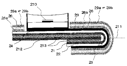
In Fig. 2-4, in the metal base circuit board of the
present invention, heat generating components 210 are
mounted on the component-mounted portions. Here, the
dotted line in Fig. 2-4 shows a bending portion 211 of
20 the metal base circuit board of the present invention.
At the bending portion 211, a slit portion 25 is formed,
whereby the board can easily be bent, and even when bent,
the conductive circuit at the bending portion is
reinforced by the coverlay 26, whereby there will be no
25 breaking or no cracking in the insulating layer.
Thus, in the metal base circuit board of the present
invention, the board is reinforced by the coverlay, and
CA 02605209 2007-10-16
41
even if it is bent, a failure such as breaking of the
conductive circuit or cracking of the insulating layer
will be prevented, and by the slit processing, it has a
substantial merit such that the bending property is good.
s Further, by the formation of the layer having a magnetic
loss or the layer having a dielectric loss, the metal
base circuit board has good electromagnetic wave
absorbing properties.
Heretofore, a metal base circuit board having a
io thickness of about 150 im has had a problem that if it is
bent at an angle of at least 900 with a radius of
curvature of at most 0.5 mm, a failure such as breaking
of the conductive circuit or cracking of the insulating
layer occurs, and it has been necessary to reinforce it
is with a coverlay. However, if it is reinforced by a
coverlay, the metal base circuit board becomes stiff, and
it becomes difficult to bend it at a desired portion.
Whereas, the present invention provides an epoch
making metal base circuit board which satisfies both the
20 bendability and reinforcement of the board against
bending and which is additionally provided with
electromagnetic absorbing properties.
Fig. 2-5 shows a schematic construction with respect
to an example of a LED module using the metal base
25 circuit board of the present invention. It is a cross-
sectional view in a case where with respect to the metal
base circuit board of Fig. 2-4, an input circuit is bent
. CA 02605209 2009-08-17
71416-378
42
at an angle of 1800 along the slit portion. In the metal
base Circuit board of the present invention, the coverlay
26 and further the layer 29a having a magnetic loss or
the layer 29b having a dielectric loss are formed via an
s epoxy adhesive layer 25a to the metal base circuit board
comprising the metal foil 21, the insulating layer 22,
the conductive circuit 23 and the electrodes 24.
In the metal base circuit board of Fig. 2-5, the
conductive circuit 23 and the electrode 24 are
lo electrically connected, and on the electrode 24, a heat
generating component 210 is mounted as electrically
connected by e.g. a solder. Further, the rear side of
the metal base circuit board is closely bonded to the
case 212 having heat dissipation performance, via a heat
15 conductive adhesive tape 213. The conductive circuit 23
and a lead wiring (input circuit) are electrically
connected, so that the electric power can be input from
the exterior to the heat generating component such as LED.
In Fig. 2-5, the board is bent to the metal foil 21
20 side, but in the present invention, it is possible to
bend it to the side of the layer 29a having a magnetic
loss or the layer 29b having a dielectric loss. So long
as, with respect to at least the coverlay at the portion
to be bent, slit processing is done from 50% to 95%
25 relative to the length of the portion to be bent, bending
can be done in various shapes depending upon the shape of
- the case '212 having heat dissipation performance.
CA 02605209 2007-10-16
43
The above-described slit processing is not limited
to the rectangular processing shown in the metal base
circuit board in Figs. 2-1 to 2-4, and it may be one
wherein the corners are acute-angled or wedge-shaped as
s shown in Fig. 2-6, or one wherein many circular holes are
formed as shown in Fig. 2-7. Circular holes may rather
be preferred, since the bending portion can thereby be
easily determined.
The LED array using the metal base circuit board of
lo the present invention has the above-described
construction, and it is preferred that the thickness of
the metal foil 21 is from 5 pm to 40 pm, the insulating
layer 22 comprises the inorganic filler and the
thermosetting resin and has a thickness of from 30 pm to
15 80 pm, and the thickness of the conductive circuit is
from 9 pm to 40 pm. When such various conditions are
satisfied, the purpose of the present invention can more
certainly be accomplished.
When the thickness of the metal foil 21 is at least
20 5 pm, there is no such a possibility that the rigidity of
the metal base circuit board deteriorates and the
application is limited. When the thickness of the metal
foil 21 is at most 40 pm, there will be no possibility
that a die for bending or a die for drawing the metal
25 base circuit board, or a processing equipment such as a
pressing machine, is required, or there will be no
possibility such that it becomes difficult to closely
CA 02605209 2007-10-16
44
bond the metal base circuit board to e.g. a curved
surface of a case. Further, there will be no difficulty
in bending at room temperature in such a state that an
electrical component such as a semiconductor element or
resistant chip which requires heat dissipation, is
mounted on the metal base circuit board. The thickness
of the metal foil 21 is more preferably from 12 pm to 35
pm, since the rigidity, bending processability, drawing
processability, etc., particularly the bending
processability at an angle of at least 900 with a radius
of curvature of from 0.1 to 0.5 mm, of the metal base
circuit board, will be thereby excellent.
In the LED array using the metal base circuit board
of the present invention, it is preferred that the
ls insulating layer 22 comprises the inorganic filler and
the thermosetting resin and has a thickness of from 30 pm
to 80 pm. With respect to the thickness of the
insulating layer 22, when it is at least 30 pm, the
insulating performance can be secured, and when it is at
most 80 pm, such is preferred since bending
processability at an angle of at least 90 with a radius
of curvature of from 0.1 to 0.5 mm will not be low.
In the LED array using the metal base circuit board
of the present invention, the thickness of the conductive
circuit is preferably from 9 pm to 40 pm. When it is at
least 9 pm, the function as a conductive circuit can
sufficiently be secured, and when it is at most 40 pm,
CA 02605209 2007-10-16
sufficient bendability can be secured, and a sufficient
thickness for small-sizing or reduction of the thickness
can be secured.
Further, the heat conductive adhesive tape 213 to be
s used in the present invention may be one having
incorporated in a polymer resin material a heat
conductive electrical insulating agent made of a metal
oxide such as aluminum oxide or titanium dioxide, a
nitride such as aluminum nitride, boron nitride or
10 silicon nitride, an inorganic substance such as silicon
carbide or aluminum hydroxide, or an organic substance
such as acrylic rubber. Further, a heat conductive
adhesive tape having one surface-treated by e.g. a silane
coupling agent incorporated in a polymer resin material,
is may also be used.
The heat conductive adhesive tape 213 is preferably
one having the heat conductivity improved over the
conventional adhesive tape, in order to efficiently
dissipate the heat generated from the heat generating
20 component from the rear side of the metal base board to
the case via the metal base circuit board.
For the heat conductive adhesive tape 213, an
adhesive tape having characteristics and the base
material used in the following "LED light source unit"
25 may suitably be used.
LED LIGHT SOURCE UNIT
A preferred embodiment of a LED light source unit
CA 02605209 2009-08-17
71416-378
46
using the metal base circuit board of the present
invention will be described.
For the LED light source unit using the metal base
circuit board of the present invention, the above-
described metal foil, inorganic filler, thermosetting
resin, conductive circuit, etc., as the main constituting
materials in the metal base circuit board can be
optionally used.
Fig. 3-1 is a cross-sectional view showing a
schematic construction with respect to an example of the
LED light source unit of the present invention.
In the LED light source unit of the present
invention, at least one LED 36 is mounted as bonded by
e.g. a solder joint portion 35 on a conductive circuit 33
ls of the metal base circuit board comprising a metal foil
31, an insulating layer 32 and the conductive circuit 33,
and the board is closely bonded to a case 38 having a
heat dissipation performance, via a heat conductive
adhesive tape 37. The conductive circuit 33 and a lead
wiring (input circuit) 34 are electrically connected, so
that the power can be input from the exterior to LED.
In Fig. 3-1, the overall shape is a box shape.
However, in the present invention, so long as the metal
foil 31, the insulating layer 32 and the conductive
circuit 33 constituting the metal base circuit board
other than the portion on which LED 36 is mounted, are
closely bonded to the case 38 having heat dissipation
CA 02605209 2007-10-16
47
performance, various shapes may be adopted to meet the
surface shape of the case 38 having the heat dissipation
performance.
The LED light source unit of the present invention
s has the above-described construction, and it is preferred
that the thickness of the metal foil 31 is from 18 pm to
300 pm, and the insulating layer 32 comprises the
inorganic filler and the thermosetting resin and has a
thickness of from 80 pm to 200 pm, and the thickness of
lo the conductive circuit 33 is from 9 pm to 140 pm.
The thickness of the metal foil 31 is preferably
from 18 pm to 300 pm. If the thickness of the metal foil
31 is less than 18 pm, the rigidity of the metal base
circuit board tends to deteriorate, and the application
15 will be limited. If the thickness exceeds 300 pm, not
only a bending die or a drawing die, or a processing
equipment such as a press machine for the metal base
circuit board will be required, but also it tends to be
difficult to bond the metal base circuit board to e.g. a
20 curved surface of a case. Further, it tends to be
difficult to carry out bending at room temperature in
such a state that an electrical component such as a
semiconductor element or resistance chip which requires
heat dissipation is mounted on the metal base circuit
25 board. The thickness is more preferably from 35 pm to 70
pm, whereby the metal base circuit board will be
excellent in the rigidity, bending processability,
CA 02605209 2007-10-16
48
drawing processability, etc., particularly in the bending
processability at an angle of at least 900 with a radius
of curvature of from 1 to 5 mm.
The insulating layer 32 comprises the inorganic
filler and the thermosetting resin, and preferably has a
thickness of from 80 pm to 200 pm. With respect to the
thickness of the insulating layer 32, if it is less than
80 pm, the insulating performance tends to be low, and if
it exceeds 200 pm, not only the heat dissipation
lo performance tends to deteriorate but also the thickness
increases, whereby small-sizing or reduction of the
thickness tends to be difficult.
In the LED light source unit of the present
invention, the thickness of the conductive circuit is
from 9 pm to 140 pm. If it is less than 9 pm, the
function as a conductive circuit tends to be inadequate,
and if it exceeds 140 pm, not only the bendability tends
to deteriorate, but also the thickness increases, whereby
small-sizing or reduction of the thickness tends to be
difficult.
The LED light source unit of the present invention
is useful even when it is repeatedly bent. Thus, its
processability is high, and it can be reused. Further,
it is possible to easily produce a LED light source unit
having a case having a curved surface by mounting LED on
the metal base circuit board, followed by bonding to a
case having a flat portion, and then processing for
CA 02605209 2007-10-16
49
deformation together with the case, and thus it will be
possible to provide a large amount of LED light source
units at low costs.
As the heat conductive adhesive tape 37 to be used
in the present invention, as described hereinafter, one
having incorporated in a polymer resin material a heat
conductive electrical insulating agent made of a metal
oxide such as aluminum oxide or titanium dioxide, a
nitride such as aluminum nitride, boron nitride or
lo silicon nitride, an inorganic substance such as silicon
carbide or aluminum hydroxide, or an organic substance
such as acrylic rubber, may be used. Further, a heat
conductive adhesive tape having one surface-treated by
e.g. a silane coupling agent incorporated in a polymer
resin material, may also be used.
With an adhesive tape having no heat conductivity,
conduction of the heat accompanied by luminance of LED to
the case tends to be inadequate, whereby the temperature
rise of LED will be brought about. Thus, such an
adhesive tape can not be used. According to the results
of the study by the present inventors, it is preferred to
use a heat conductive adhesive tape having a heat
conductivity of from 1 to 2 W/mK and having a thickness
of from 50 to 150 pm.
The heat conductive adhesive tape 37 is
characterized in that the heat conductivity is improved
over the conventional adhesive tape, so that the heat
CA 02605209 2007-10-16
generated at the time of the light emission of LED is
effectively dissipated from the rear side of the metal
base board to the case via the metal base circuit board.
The polymer material to be used for the heat
5 conductive adhesive tape 37 is not particularly limited.
However, in order to improve the adhesion to a metal, a
polymer containing acrylic acid and/or methacrylic acid
is preferably selected. Namely, an acrylate or
methacrylate having a C2_12 alkyl group or a C2_12
10 alkylester of acrylic acid or methacrylic acid, is
preferred.
From the viewpoint of the flexibility and
processability, as the monomer, it is preferred to use
one or more members selected from ethyl acrylate, propyl
15 acrylate, butyl acrylate, 2-ethylhexyl acrylate, octyl
acrylate, isooctyl acrylate, decyl acrylate, decyl
(meth)acrylate and dodecyl (meth)acrylate. Among them,
2-ethylhexyl acrylate is more preferred as the monomer.
The heat conductive adhesive tape 37 preferably
20 contains a heat conductive electrical insulating agent.
The heat conductive electrical insulating agent may be
any material so long as it is an inorganic or organic
substance having good heat conductivity and electrical
insulting properties. As an organic substance, natural
25 rubber, or a rubber such as NBR or EPDM is preferred, and
particularly preferred is one containing acrylic rubber.
Such a heat conductive electrical insulating agent is
CA 02605209 2009-08-17
71416-378
51
preferably contained in an amount of from 40 to 80 vol%
in the adhesive tape 37, whereby good heat dissipation
performance can be secured. From SO to 70 vol% is a more
preferred range.
The monomer for such acrylic rubber may, for example,
be ethyl acrylate, n-propyl acrylate, n-butyl acrylate,
isobutyl acrylate, n-pentyl acrylate, isoamyl acrylate,
n-hexyl acrylate, 2-methylpentyl acrylate, n-octyl
acrylate, 2-ethylhexyl acrylate, n-decyl acrylate, n-
dodecyl acrylate, n-octadecyl acrylate, cyanomethyl
acrylate, 1-cyanoethyl acrylate, 2-cyanoethyl acrylate,
1-cyanopropyl acrylate or 2-cyanopropyl acrylate. A
combination of more than one selected among these, or
acrylic rubber having a few % of a crosslinkable monomer
is copolymerized, is preferred. The rubber content is
preferably from 0.1 to 30 parts by mass in the heat
conductive adhesive tape 37. If it is less than 0.1 part
by mass, when a highly heat conductive filler is
incorporated in the polymer resin material, the filler
will be precipitated, and if it exceeds 30 parts by mass,
the viscosity tends to rise, thus leading to a problem
during the processing. When the rubber content is from
0.1 to 30 parts by mass, the processability is good,
while precipitation of the filler is prevented.
As such a monomer, from the viewpoint of the
flexibility and adhesive property, an acrylate or
methacrylate having a C2_12 alkyl group, or a C2_12 acryl
CA 02605209 2007-10-16
52
ester of acrylic acid is preferred. From the viewpoint
of the flexibility and processability, a preferred
monomer is one or a blend of two or more selected from
ethyl acrylate, propyl acrylate, butyl acrylate, 2-
ethylhexyl acrylate, octyl acrylate, isooctyl acrylate,
decyl acrylate, decyl methacrylate and dodecyl
methacrylate. A more preferred monomer is 2-ethylhexyl
acrylate.
The inorganic substance to be used as the heat
lo conductive electrical insulating agent may, for example,
be a metal oxide such as aluminum oxide or titanium
dioxide, a nitride such as aluminum nitride, boron
nitride or silicon nitride, silicon carbide or aluminum
hydroxide. Among them, it is preferably at least one
is member selected from the group consisting of alumina,
crystalline silica and aluminum hydroxide. Further, it
is also possible to select one having the surface treated
by e.g. a silane coupling agent.
Further, with respect to the size of the heat
20 conductive electrical insulating agent, it is preferred
that the maximum particle size is at most 45 pm, and the
average particle size is from 0.5 to 30 pm, from the
viewpoint of the incorporation and the thickness of the
adhesive tape.
25 The heat conductive adhesive tape 37 may contain
known polymer compounds within a range not to impair the
properties desired by the present invention. Further, at
CA 02605209 2007-10-16
53
the time of curing the heat conductive adhesive tape 37,
known additives may be incorporated as the case requires,
within a non-influential range. As such additives, for
example, various additives to control the viscosity or
adhesiveness, and others such as a modifier, and an aging
preventive agent, a heat stabilizer and a coloring agent,
may, for example, be mentioned.
The heat conductive adhesive tape 37 can be cured by
a common method. For example, it may be cured by a
method such as heat polymerization by means of a heat
polymerization initiator, photopolymerization by means of
a photopolymerization initiator or polymerization using a
heat polymerization initiator and a curing accelerator.
However, from the viewpoint of the productivity, etc.,
is photopolymerization by means of a photopolymerization
initiator is preferred.
EXAMPLES
Now, the present invention will be described with
reference to Examples. However, it should be understood
that the present invention is by no means restricted by
such specific Examples.
METAL BASE CIRCUIT BOARD
EXAMPLE 1-1
As shown in Table 1-1, to 100 parts by mass of a
bisphenol A epoxy resin having an epoxy equivalent of 187
(EPICLON830-S, manufactured by Dainippon Ink and
CA 02605209 2007-10-16
54
Chemicals Incorporated), 63 parts by mass of a
polyoxypropylenediamine (mass ratio of D-40 to D-2000 was
6:4, manufactured by HARTZMAN) was added as a curing
agent, and pulverized aluminum oxide having an average
s particle size of 2.2 pm and a maximum particle size of 20
pm (AL-173, manufactured by Showa Denko K.K.) was blended
so that it would be 50 vol% in an insulating layer, and
an insulating layer was formed on an aluminum foil having
a thickness of 40 pm so that the thickness after the
lo curing would be 100 pm. Then, an electrolytic copper
foil having a thickness of 35 pm was bonded, followed by
heating to thermally cure the insulating layer thereby to
obtain a metal base board. Further, with the obtained
metal base substrate, predetermined positions were masked
ls with an etching resist, the copper foil was then
subjected to etching, and then, the etching resist was
removed to form a circuit thereby to obtain a metal base
circuit board.
With respect to the obtained metal base circuit, (1)
20 bendability at room temperature, (2) heat conductivity of
the insulating layer, (3) bond strength between the
conductive circuit and the insulating layer, (4) glass
transition temperature of the insulating layer, (5)
breakdown voltage of the insulating layer after heat
25 treatment at 260 C for 10 minutes, (6) withstand voltage
of the insulating layer in a state bent at 90 at room
temperature, (7) breakdown time of the insulating layer
CA 02605209 2007-10-16
when a DC voltage of 1,000 V (pattern side +) was applied
at 125 C, and (8) presence or absence of cracking in the
insulating layer in a state bent at 90 at room
temperature, were determined by the following methods.
The results are shown in Table 1-2. The obtained
metal base circuit board was good in each physical
property.
(1) The bendability at room temperature was evaluated in
such a manner that the metal base circuit board was
lo processed into 10 mm x 100 mm, and one capable of being
bent at an angle of at least 90 with a radius of
curvature of 5 mm to the conductive circuit-formed
surface side and the side opposite to the conductive
circuit-formed surface by both hands in a temperature
ls atmosphere of 25+1 C, was regarded as "good" and a case
where it was necessary to use e.g. a bending die and
press machine at the time of carrying out the bending,
was regarded as "no good".
(2) Measurement of the heat conductivity was carried out
20 in such a manner that the metal foil and the conductive
circuit as base materials of the metal base circuit board
were removed, and the insulating layer was processed into
10 mm in diameter x 100 pm (partially 60 pm), and the
heat conductivity was obtained by a laser flash method.
25 (3) The bond strength between the conductive circuit and
the insulating layer was obtained by the method
prescribed in JIS C6481 by processing the conductive
CA 02605209 2007-10-16
56
circuit of the metal base circuit board into a strip with
a width of 10 mm.
(4) Measurement of the glass transition temperature (Tg)
was carried out in such a manner that the metal foil and
s the conductive circuit as base materials of the metal
base circuit board were removed, the insulating layer was
processed into 5 mm x 50 mm x 100 pm (partially 60 pm),
and the glass transition temperature was obtained by a
dynamic elasticity measuring method.
(5) Measurement of the withstand voltage of the
insulating layer after heating at 260 C for 10 minutes
was carried out in such a manner that a metal base
circuit board having a conductive circuit formed in a
circular pattern of 20 mm in diameter was put in a solder
is tank heated at 260 C, treated for 10 minutes and then
cooled to room temperature, whereupon the withstand
voltage between the circular pattern and the aluminum
foil was measured by a stepwise pressure raising method
prescribed in JIS C2110.
(6) Measurement of the withstand voltage of the
insulating layer in a state bent at 90 at room
temperature was carried out in such a manner that a metal
base circuit board having a conductive circuit formed in
a circular pattern of 20 mm in diameter, was bent at 90
with a radius of curvature of 1 mm so that the circular
pattern of 20 mm in diameter was contained, and in that
bent state, the withstand voltage between the circular
CA 02605209 2007-10-16
57
pattern and the aluminum foil was measured by a
stepwisely pressure-raising method prescribed in JIS
C2110.
(7) Measurement of the breakdown time of the insulating
layer when a DC voltage of 1,000 V (pattern side +) was
applied at 125 C, was carried out in such a manner that
by setting the circular pattern side of the metal base
circuit board having the circuit board formed in the
circular pattern of 20 mm in diameter, to be + and the
lo metal foil side to be -, a DC voltage of 1,000 V was
applied at 125 C, whereby the breakdown time of the
insulating layer was measured.
(8) The presence or absence of cracking in the
insulating layer in a state bent at 90 C at room
temperature, was visually observed.
EXAMPLE 1-2
As shown in Table 1-1, to 100 parts by mass of a
hydrogenated (in Table 1, identified by Hydrogenated)
bisphenol A epoxy resin having an epoxy equivalent of 201
(YX-8000, manufactured by Japan Epoxy Resins Co., Ltd.),
63 parts by mass of a polyoxypropylenediamine (mass ratio
of D-400 to D-2000 was 6:4, manufactured by HARTZMAN) was
added as a curing agent, and pulverized aluminum oxide
having an average particle size of 2.2 pm and a maximum
particle size of 20 pm (AL-173, manufactured by Showa
Denko K.K.) was blended so that it would be 50 vol% in an
insulting layer, and an insulating layer was formed on an
CA 02605209 2007-10-16
58
aluminum foil having a thickness of 40 pm so that the
thickness after curing would be 100 pm. Then, an
electrolytic copper foil having a thickness of 35 pm was
bonded, followed by heating to thermally cure the
insulating layer thereby to obtain a metal base board.
Except for the above, in the same manner as in Example 1-
1, a metal base circuit board was prepared, and various
physical properties were measured.
The results are shown in Table 1-2. Due to a
lo decrease of the glass transition temperature (Tg) of the
insulating layer, the bendability at room temperature was
remarkably improved. Other physical properties were also
good.
EXAMPLE 1-3
As shown in Table 1-1, to 100 parts by mass of an
epoxy resin comprising 70 mass% of a hydrogenated
bisphenol A epoxy resin having an epoxy equivalent of 201
(YX-8000, manufactured by Japan Epoxy Resins Co., Ltd.)
and 30 mass% of a bisphenol A epoxy resin having an epoxy
equivalent of 1,900 (YD-927H, manufactured by Tohto Kasei
Co., Ltd.), 48 parts by mass of a polyoxypropylenediamine
(mass ratio of D-400 to D-2000 was 6:4, manufactured by
HARTZMAN) was added as a curing agent, and pulverized
aluminum oxide having an average particle size of 2.2 pm
and a maximum particle size of 20 pm (AL-173,
manufactured by Showa Denko K.K.) was blended so that it
would be 50 vol% in an insulting layer, and an insulating
CA 02605209 2007-10-16
59
layer was formed on an aluminum foil having a thickness
of 40 pm, so that the thickness after curing would be 100
pm. Then, an electrolytic copper foil having a thickness
of 35 pm was bonded, followed by heating to thermally
s cure the insulating layer thereby to obtain a metal base
board. Except for the above, in the same manner as in
Example 1-1, a metal base circuit board was prepared, and
various physical properties were measured.
The results are shown in Table 1-2. With the
lo obtained metal base circuit board, the bond strength
between the conductive circuit and the insulating layer
was remarkably improved. Other physical properties were
also good.
EXAMPLE 1-4
15 As shown in Table 1-1, to 100 parts by mass of an
epoxy resin comprising 70 mass% of a hydrogenated
bisphenol A epoxy resin having an epoxy equivalent of 201
(YX-8000, manufactured by Japan Epoxy Resins Co., Ltd.)
and 30 mass% of a hydrogenated bisphenol A epoxy resin
20 having an epoxy equivalent of 1,024 (ST-4100D,
manufactured by Tohto Kasei Co., Ltd.), 50 parts by mass
of a polyoxypropylenediamine (mass ratio of D-400 to D-
2000 was 6:4, manufactured by HARTZMAN) was added as a
curing agent, and pulverized aluminum oxide having an
25 average particle size of 2.2 pm and a maximum particle
size of 20 pm (AL-173, manufactured by Showa Denko K.K.)
was blended so that it would be 50 vol% in an insulting
CA 02605209 2007-10-16
layer, and an insulating layer was formed on an aluminum
foil having a thickness of 40 pm, so that the thickness
after curing would be 100 pm. Then, an electrolytic
copper foil having a thickness of 35 pm was bonded,
s followed by heating to thermally cure the insulating
layer, thereby to obtain a metal base board. Except for
the above, in the same manner as in Example 1-1, a metal
base circuit board was prepared, and various physical
properties were measured.
10 The results are shown in Table 1-2. With the
obtained metal base circuit board, in addition to the
bond strength between the conductive circuit and the
insulating layer, the bendability at room temperature was
remarkably improved due to a decrease in the glass
15 transition temperature (Tg). Other physical properties
were also good.
EXAMPLE 1-5
As shown in Table 1-1, to 100 parts by mass of an
epoxy resin comprising 70 mass%, based on the entire
20 epoxy resin, of a hydrogenated bisphenol F epoxy resin
having an epoxy equivalent of 181 (YL-6753, manufactured
by Japan Epoxy Resins Co., Ltd.) and 30 mass% of a
hydrogenated bisphenol A epoxy resin having an epoxy
equivalent of 1,024 (ST-4100D, manufactured by Tohto
25 Kasei Co., Ltd.), 55 parts by mass of a
polyoxypropylenediamine (mass ratio of D-400 to D-2000
was 6:4, manufactured by HARTZMAN) was added as a curing
CA 02605209 2007-10-16
61
agent, and pulverized aluminum oxide having an average
particle size of 2.2 pm and a maximum particle size of 20
pm (AL-173, manufactured by Showa Denko K.K.) was blended
so that it would be 50 vol% in an insulting layer, and an
insulating layer was formed on an aluminum foil having a
thickness of 40 pm, so that the thickness after curing
would be 100 pm. Then, an electrolytic copper foil
having a thickness of 35 pm was bonded, followed by
heating to thermally cure the insulating layer, thereby
lo to obtain a metal base board. Except for the above, in
the same manner as in Example 1-1, a metal base circuit
board was prepared, and various physical properties were
measured.
The results are shown in Table 1-2. With the
obtained metal base circuit board, in addition to the
bond strength between the conductive circuit and the
insulating layer, the bendability at room temperature was
remarkably improved due to a decrease in the glass
transition temperature (Tg).
EXAMPLE 1-6
As shown in Table 1-1, to 100 parts by mass of an
epoxy resin comprising 70 mass%, based on the entire
epoxy resin, of a hydrogenated bisphenol A epoxy resin
having an epoxy equivalent of 207 (EXA-7015, manufactured
by Dainippon Ink and Chemicals Incorporated), and 30
mass% of a hydrogenated bisphenol A epoxy resin having an
epoxy equivalent of 1,200 (YL-7170, manufactured by Japan
CA 02605209 2007-10-16
62
Epoxy Resins Co., Ltd.), 48 parts by mass of a
polyoxypropylenediamine (mass ratio of D-400 to D-2000
was 6:4, manufactured by HARTZMAN) was added as a curing
agent, and pulverized aluminum oxide having an average
particle size of 2.2 pm and a maximum particle size of 20
pm (AL-173, manufactured by Showa Denko K.K.) was blended
so that it would be 50 vol% in an insulting layer, and an
insulating layer was formed on an aluminum foil having a
thickness of 40 pm, so that the chloride ion
concentration would be 250 ppm in the entire
thermosetting resin, and the thickness after curing would
be 100 pm. Then, an electrolytic copper foil having a
thickness of 35 pm was bonded, followed by heating to
thermally cure the insulating layer thereby to obtain a
metal base board. Except for the above, in the same
manner as in Example 1-1, a metal base circuit board was
prepared, and various physical properties were measured.
The results are shown in Table 1-2. With the
obtained metal base circuit board, in addition to the
bond strength between the conductive circuit and the
insulating layer, the bendability at room temperature was
remarkably improved due to a decrease in the glass
transition temperature (Tg). Further, the breakdown time
of the insulating layer when a DC voltage of 1,000 V
(pattern side+) was applied at 125 C, was extended.
Other physical properties were also good.
EXAMPLE 1-7
CA 02605209 2007-10-16
63
As shown in Table 1-1, to 100 parts by mass of an
epoxy resin comprising 70 mass%, based on the entire
epoxy resin, of a hydrogenated bisphenol A epoxy resin
having an epoxy equivalent of 207 (EXA-7015, manufactured
by Dainippon Ink and Chemicals Incorporated) and 30 mass%
of a hydrogenated bisphenol A epoxy resin having an epoxy
equivalent of 1,200 (YL-7170, manufactured by Japan Epoxy
Resins Co., Ltd.), 48 parts by mass of a
polyoxypropylenediamine (mass ratio of D-400 to D-2000
lo was 6:4, manufactured by HARTZMAN) was added as a curing
agent, and spherical coarse particles of aluminum oxide
having a maximum particle size of at most 75 pm, an
average particle size of 21 pm and a sodium ion
concentration of 10 ppm (CB-A20, manufactured by Showa
Denko K.K.) and spherical fine particles of aluminum
oxide having an average particle size of 0.7 pm and a
sodium ion concentration of 8 ppm (AKP-15, manufactured
by Sumitomo Chemical Co., Ltd.) were blended so that the
total amount would be 50 vol% in an insulating layer
(mass ratio of spherical coarse particles to spherical
fine particles was 7:3), and an insulating layer was
formed on an aluminum foil having a thickness of 40 pm,
so that the thickness after curing would be 100 pm. Then,
an electrolytic copper foil having a thickness of 35 pm
was bonded, followed by heating to thermally cure the
insulating layer to obtain a metal base board having a
chloride ion concentration in the insulating layer of at
CA 02605209 2007-10-16
64
most 300 ppm based on the entire thermosetting resin and
a sodium ion concentration in the insulating layer of at
most 50 ppm based on the entire inorganic filler. Except
for the above, in the same manner as in Example 1-1, a
metal base circuit board was prepared, and the respective
physical properties were measured.
The results are shown in Table 1-2. With the
obtained metal base circuit board, the breakdown time of
the insulating layer when a DC voltage of 1,000 V
(pattern side+) was applied at 125 C, was remarkably
extended, and other physical properties were also good.
EXAMPLE 1-8
As shown in Table 1-1, to 100 parts by mass of an
epoxy resin comprising 70 mass% of 170 ppm hydrogenated
bisphenol A epoxy resin having an epoxy equivalent of 207
(EXA-7015, manufactured by Dainippon Ink and Chemicals
Incorporated) and 30 mass% of a hydrogenated bisphenol A
epoxy resin having an epoxy equivalent of 1,200 (YL-7170,
manufactured by Japan Epoxy Resins Co., Ltd.), 48 parts
by mass of a polyoxypropylenediamine (mass ratio of D-400
to D-2000 was 6:4, manufactured by HARTZMAN) was added as
a curing agent, and spherical coarse particles of
aluminum oxide having a maximum particle size of at most
75 pm, an average particle size of 21 pm and a sodium ion
concentration of 10 ppm (CB-A20, manufactured by Showa
Denko K.K.) and spherical fine particles of aluminum
oxide having an average particle size of 0.7 pm and a
CA 02605209 2007-10-16
sodium ion concentration of 8 ppm (AKP-15, manufactured
by Sumitomo Chemical Co., Ltd.) were blended so that the
total amount would be 66 vol% in an insulating layer
(mass ratio of spherical coarse particles to spherical
s fine particles was 7:3), and an insulating layer was
formed on an aluminum foil having a thickness of 40 pm,
so that the thickness after curing would be 100 pm. Then,
an electrolytic copper foil having a thickness of 35 pm
was bonded, followed by heating to thermally cure the
lo insulating layer to obtain a metal base board having a
chloride ion concentration in the insulating layer of at
most 300 ppm based on the entire thermosetting resin and
a sodium ion concentration in the insulating layer of at
most 60 ppm based on the entire inorganic filler. Except
15 for the above, in the same manner as in Example 1-1, the
metal base circuit board was prepared, and various
physical properties were measured.
The results are shown in Table 1-2. With the
obtained metal base circuit board, the heat conductivity
20 was further improved, and other physical properties were
also good.
COMPARATIVE EXAMPLE 1-1
As shown in Table 1-1, to 100 parts by mass of a
bisphenol A epoxy resin having an epoxy equivalent of 187
25 (EPICLON 850-S, manufactured by Dainippon Ink and
Chemicals Incorporated), 63 parts by mass of a
polyoxypropylenediamine (mass ratio of D-400 to D-2000
CA 02605209 2007-10-16
66
was 6:4, manufactured by HARTZMAN) was added as a curing
agent, and a pulverized aluminum oxide having an average
particle size of 2.2 pm and a maximum particle size of 20
pm (AL-173, manufactured by Showa Denko K.K.) was blended
so that it would be 80 vol% in an insulating layer, and
an insulating layer was formed on an aluminum foil having
a thickness of 400 pm, so that the thickness after curing
would be 100 pm. Then, a copper foil having a thickness
of 210 pm was bonded, followed by heating to thermally
lo cure the insulating layer to obtain a metal base board.
Except for the above, in the same manner as in Example 1-
1, a metal base circuit board was prepared, and various
physical properties were measured.
The results are shown in Table 1-2. The obtained
metal base circuit board had no substantial bendability,
could not be manually bent at room temperature and was
bent at 90 by means of a bending die and a pressing
machine. Further, the bond strength between the
conductive circuit and the insulating layer was weak, and
the withstand voltage of the insulating layer in a state
bent at 90 at room temperature was extremely low.
Further, the breakdown time of the insulating layer when
a DC voltage of 1,000 V (pattern side+) was applied at
125 C, was also extremely short. Further, the heat
conductivity was partially different, and its fluctuation
was large.
COMPARATIVE EXAMPLE 1-2
CA 02605209 2007-10-16
67
As shown in Table 1-1, to 100 parts by mass of a
bisphenol A epoxy resin having an epoxy equivalent of 187
(EPICLON 850-S, manufactured by Dainippon Ink and
Chemicals Incorporated), 63 parts by mass of a
polyoxypropylenediamine (mass ratio of D-400 to D-2000
was 6:4, manufactured by HARTZMAN) was added as a curing
agent, and a pulverized aluminum oxide having an average
particle size of 57 pm and a maximum particle size of 90
pm (A-13-L, manufactured by Showa Denko K.K.) was blended
lo so that it would be 50 vol% in an insulating layer, and
an insulating layer was formed on an aluminum foil having
a thickness of 40 pm, so that the thickness after curing
would be 60 pm. Then, an electrolytic copper foil having
a thickness of 35 pm was bonded, followed by heating to
thermally cure the insulating layer thereby to obtain a
metal base board. Except for the above, in the same
manner as in Example 1-1, a metal base circuit board was
prepared, and various physical properties were measured.
The results are shown in Table 1-2. With the
obtained metal base circuit board, many irregularities
which appeared to be projections of the alumina filler,
were observed at the insulating layer-exposed portion on
the conductive circuit surface, and cracking was observed
in the insulating layer when bent at room temperature.
Further, the bond strength between the conductive circuit
and the insulating layer was weak, and the withstand
voltage of the insulating layer in a state bent at 90 at
CA 02605209 2007-10-16
68
room temperature was extremely low. Further, the
breakdown time of the insulating layer when a DC voltage
of 1,000 V (pattern side+) was applied at 125 C, was also
extremely short.
s COMPARATIVE EXAMPLE 1-3
As shown in Table 1-1, to 100 parts by mass of an
epoxy resin comprising 40 mass % of a bisphenol A epoxy
resin having an epoxy equivalent of 187 (EPICLON 850-S,
manufactured by Dainippon Ink and Chemicals Incorporated)
lo and 60 mass% of a bisphenol A epoxy resin having an epoxy
equivalent of 4,000 (EPIKOTE 1010, manufactured by Japan
Epoxy Resins Co., Ltd.), 51 parts by mass of a
polyoxypropylenediamine (mass ratio of D-400 to D-2000
was 6:4, manufactured by HARTZMAN) was added as a curing
15 agent, and pulverized aluminum oxide having an average
particle size of 2.2 pm and a maximum particle size of 20
pm (AL-173, manufactured by Showa Denko K.K.) was blended
so that it would be 50 vol% in an insulating layer, and
an insulating layer was formed on an aluminum foil having
20 a thickness of 400 pm, so that the thickness after curing
would be 100 pm. Then, an electrolytic copper foil
having a thickness of 35 pm was bonded, followed by
heating to thermally cure the insulating layer thereby to
obtain a metal base board. Except for the above, in the
25 same manner as in Example 1-1, a metal base circuit board
was prepared, and various physical properties were
measured.
CA 02605209 2007-10-16
69
The results are shown in Table 1-2. The obtained
metal base circuit board had no substantial bendability
and could not be manually bent at room temperature. It
was bent at 90 by means of a bending die and a pressing
machine, whereby the glass transition temperature (Tg)
rised, and the bendability at room temperature was
inadequate, and the withstand voltage of the insulating
layer in a state bent at 90 at room temperature was
remarkably low.
lo COMPARATIVE EXAMPLE 1-4
As shown in Table 1-1, to 100 parts by mass of an
epoxy resin comprising 70 mass% of a hydrogenated
bisphenol A epoxy resin having an epoxy equivalent of 238
and a chloride ion concentration in the resin of 1,500
ppm (EPOLIGHT 4000, manufactured by KYOEISHA CHEMICAL CO.,
LTD.) and 30 mass% of a bisphenol F epoxy resin having an
epoxy equivalent of 1,200 and a chloride ion
concentration in the resin of 920 ppm (EPIKOTE 4004P,
manufactured by Japan Epoxy Resins Co., Ltd.), 42 parts
by mass of a polyoxypropylenediamine (mass ratio of D-400
to D-2000 was 6:4, manufactured by HARTZMAN) was added as
a curing agent, and pulverized aluminum oxide having an
average particle size of 2.2 pm and a maximum particle
size of 20 pm (AL-173, manufactured by Showa Denko K.K.)
was blended so that it would be 50 vol% in an insulating
layer, and an insulating layer was formed on an aluminum
foil having a thickness of 400 pm, so that the thickness
CA 02605209 2007-10-16
after curing would be 100 pm, and the chloride ion
concentration was 1,000 ppm based on the entire
thermosetting resin. Then, an electrolytic copper foil
having a thickness of 35 pm was bonded, followed by
s heating to thermally cure the insulating layer thereby to
obtain a metal base board. Except for the above, in the
same manner as in Example 1-1, a metal base circuit board
was prepared, and various physical properties were
measured.
10 The results are shown in Table 1-2. With the
obtained metal base circuit board, the breakdown time of
the insulating layer when a DC voltage of 1,000 V
(pattern side+) was applied at 125 C, was extremely short.
COMPARATIVE EXAMPLE 1-5
15 As shown in Table 1-1, to 100 parts by mass of an
epoxy resin comprising 70 mass% of a hydrogenated
bisphenol A epoxy resin having an epoxy equivalent of 238
and a chloride ion concentration in the resin of 1,500
ppm (EPOLIGHT 4000, manufactured by KYOEISHA CHEMICAL CO.,
20 LTD.) and 30 mass% of a bisphenol F epoxy resin having an
epoxy equivalent of 1,200 and a chloride ion
concentration in the resin of 920 ppm (EPIKOTE 4004P,
manufactured by Japan Epoxy Resins Co., Ltd.), 63 parts
by mass of a polyoxypropylenediamine (mass ratio of D-400
25 to D-2000 was 6:4, manufactured by HARTZMAN) was added as
a curing agent, and spherical coarse particles of
aluminum oxide having a maximum particle size of at most
CA 02605209 2007-10-16
71
75 pm, an average particle size of 25 pm and a sodium ion
concentration of 530 ppm (AX-25, manufactured by MICRON
Co., Ltd.) and spherical fine particles of aluminum oxide
having an average particle size of 1.2 pm and a sodium
ion concentration of 396 ppm (AW15-25, manufactured by
MICRON Co., Ltd.) were blended so that the total amount
would be 50 wt% in an insulating layer (mass ratio of
spherical coarse particles to spherical fine particles
was 7:3), and an insulating layer was formed on an
aluminum foil having a thickness of 400 pm, so that the
thickness after curing would be 100 pm. Then, an
electrolytic copper foil having a thickness of 35 pm was
bonded, followed by heating to thermally cure the
insulating layer to obtain a metal base board having a
is chloride ion concentration of 1,000 ppm, based on the
entire thermosetting resin, in the insulating layer and a
sodium ion concentration of 500 ppm, based on the entire
inorganic filler, in the insulating layer. Except for
the above, in the same manner as in Example 1-1, a metal
base circuit board was prepared, and various physical
properties were measured.
The results are shown in Table 1-2. With the
obtained metal base circuit board, the breakdown time of
the insulating layer when a DC voltage of 1,000 V was
applied at 125 C, was remarkably short.
The thickness of each layer of the metal base
circuit substrate, the type and amount of the
CA 02605209 2007-10-16
72
thermosetting resin, the contained chloride ion
concentration, the type of the inorganic filler and the
contained sodium ion concentration, are shown in Table 1-
1.
Various physical properties of the prepared metal
base circuit boards are shown in Table 1-2.
TABLE 1-1
Thickness of metal base
Types and amounts of thermosetting resins
circuit board
Epoxy resin (1)
Metal Conductive
foil
Content in
Insulating circuit Epoxy Chloride ion
layer (pm) Type equivalent concentration
epoxy
(pm) (Pm)
resin
(g/eq)
(PPm) (mass%)
Example 1-1 40 100 35 Bisphenol A
187 700 100
Hydrogenated
Example 1-2 40 100 35 201
700 100
bisphenol A
Hydrogenated
Example 1-3 40 100 35 201
700 70 n
bisphenol A
0
Hydrogenated I.)
Example 1-4 40 100 35 201
700 70 m
bisphenol A 0
m
I.)
Hydrogenated 0
Example 1-5 40 100 35 181
700 70 ko
bisphenol F I.)
-õ3
0
Hydrogenated w 0
Example 1-6 40 100 35 207
170 70
1
bisphenol A H
0
I
Hydrogenated H
Example 1-7 40 100 35 207
170 70 m
bisphenol A
Hydrogenated
Example 1-8 40 100 35 207
170 70
bisphenol A
Comparative
400 100 210 Bisphenol A 187
700 100
Example 1-1
Comparative
40 60 35 Bisphenol A 187
700 100
Example 1-2
Comparative
400 100 35 Bisphenol A 187
700 40
Example 1-3
Comparative Hydrogenated
400 100 35 238 1500
70
Example 1-4 bisphenol A
._
Comparative Hydrogenated
400 100 35 238 1500
70
Example 1-5 bisphenol A
TABLE 1-1 (continued)
Types and amounts of thermosetting resins
Epoxy resin (2) Chloride ion
concentration
Epoxy Chloride ion Content in
in
Type equivalent concentration epoxy resin
thermosetting
(g/eq) (PPm) (mass%)
resin (ppm)
Example 1-1 - - - -
450
Example 1-2 - - - -
460
Example 1-3 Bisphenol A 1900 630 30
490
Hydrogenated
Example 1-4 1024 810 30
500
bisphenol A
n
Hydrogenated
0
Example 1-5 1024 810 30
500
"
bisphenol A
m
0
m
Hydrogenated
"
Example 1-6 1200 250 30
180 0
ko
bisphenol A
I.)
Hydrogenated
Example 1-7 1200 250 30
180
--3
1
bisphenol A
H
0
Hydrogenated
1
1200 250 30 180
H
Example 1-8 bisphenol A
m
Comparative
- - - -
450
Example 1-1
Comparative
- - - -
450
Example 1-2
Comparative
Bisphenol A 4000 700 60
480
Example 1-3
Comparative
Bisphenol F 1200 920 30
1000
Example 1-4 .
Comparative
Bisphenol F 1200 920 30
1000
Example 1-5
TABLE 1-1 (continued)
Inorganic filler (aluminum oxide)
Inorganic filler (1) Inorganic filler (2) Content of
Sodium ion
Sodium ion inorganic filler in
Type concentration Type
concentration insulating layer
(PPrn)
(Plorn) (vol%)
_
Example 1-1 Pulverized 230 -
- 50
Example 1-2 Pulverized 230 -
- 50
Example 1-3 Pulverized 230 -
- 50
Example 1-4 Pulverized 230 -
- 50
Example 1-5 Pulverized 230 -
- 50
Example 1-6 Pulverized 230 -
- 50 0
Example 1-7Spherical coarse Spherical fine 0
I.)
8 50 m
particles particles
0
m
I.)
Example 1 10 -8Spherical coarse
Spherical fine 0
8 66
particles particles
0
Comparative
0
Pulverized 230
-- 80 --3
1
Example 1-1
H
0
I
Comparative
H
Example 1-2 Pulverized 230 -
- 50 m
Comparative
Example 1-3 Pulverized 230 -
- 50
Comparative
Example 1-4 Pulverized 230 -
- 50
ComparativeSpherical coarse Spherical fine
530 396 50
Example 1-5 particles particles
TABLE 1-2
Heat conductivity Bond strength between
Glass transition
Bendability at of insulating conductive circuit and
temperature of
room temperature layer insulting layer
insulating layer (Tg)
(W/mK) (N/cm2)
( C)
Example 1-1 Good 2.0 16.0
38.0
Example 1-2 Good 2.0 10.0
8.0
Example 1-3 Good 2.0 25.0
28.0
Example 1-4 Good 2.0 23.0
18.0
Example 1-5 Good 2.0 22.0
16.0
Example 1-6 Good 2.0 20.0
20.0
0
Example 1-7 Good 2.0 20.0
20.0
0
Example 1-8 Good 4.0 20.0
21.0 I.)
m
0
Comparative
....3 in
No good 3.0 5.1
38.0
Example 1-1
0
ko
Comparative
I.)
No good 2.0 20.0
38.0 0
Example 1-2
0
--3
1
Comparative
H
No good 2.0 20.3
80.0 0
1
Example 1-3
H
m
Comparative
No good 2.0 18.1
20.0
Example 1-4
Comparative
No good 2.0 17.5
20.0
Example 1-5
TABLE 1-2 (continued)
Breakdown voltage Breakdown time
when Presence or absence
Breakdown voltage in
after heat DC voltage of
1,000 of cracking in the
a state bent at 900
treatment at 260 C V was applied at insulating layer when
at room temperature
for 10 min. 125 C
bent at 90 at room
(kV) (kV) (hr)
temperature
Example 1-1 4.0 4.0 1200
Absent
Example 1-2 3.5 4.0 1050
Absent
Example 1-3 4.0 4.0 1300
Absent
Example 1-4 4.0 3.8 1020
Absent
Example 1-5 4.0 4.0 1030
Absent
0
Example 1-6 3.5 2.5 51000
Absent
Example 1-7 4.5 5.0 103000
Absent 0
I.)
m
Example 1-8 3.5 4.0 98000
Absent 0
in
I.)
Comparative
õJ 0
1.2 0.5 490
Present
Example 1-1
I.)
0
0
Comparative
--]
1.3 0.8 510
Present 1
Example 1-2
H
0
I
Comparative
H
3.0 0.5 1210
Present m
Example 1-3
Comparative
1.0 0.7 302
Absent
Example 1-4
Comparative
1.0 0.7 194
Absent
Example 1-5
CA 02605209 2007-10-16
78
MULTILAYER CIRCUIT BOARD
EXAMPLE 2-1
To 100 parts by mass of an epoxy resin comprising 70
mass%, based on the entire epoxy resin, of a hydrogenated
s bisphenol A epoxy resin having an epoxy equivalent of 201
("XY-8000", manufactured by Japan Epoxy Resins Co., Ltd.)
and 30 mass% of a hydrogenated bisphenol A epoxy resin
having an epoxy equivalent of 1,200 ("YL-7170",
manufactured by Japan Epoxy Resins Co., Ltd.), 48 parts
lo by mass of a polyoxypropylenediamine (mass ratio of "D-
400" to "D-2000" was 6:4, manufactured by HARTZMAN) was
added as a curing agent, and spherical coarse particles
of aluminum oxide having a maximum particle size of at
most 75 pm and an average particle size of 21 pm ("CB-
15 A20", manufactured by Showa Denko K.K.) and spherical
fine particles of aluminum oxide having an average
particle size of 0.6 pm ("A0-802", manufactured by
Admatechs Corporation) were blended so that the total
amount would be 50 vol% in an insulating layer (mass
20 ratio of spherical coarse particles to spherical fine
particles was 6:4), and an insulating layer was formed on
a copper foil having a thickness of 35 pm, so that the
thickness after curing would be 100 pm. Then, a copper
foil having a thickness of 35 pm was bonded, followed by
25 heating to thermally cure the insulating layer to obtain
an inner layer foil-laminated board.
Further, with respect to the obtained board,
CA 02605209 2007-10-16
79
predetermined positions were masked with a dry film, and
the copper foil was subjected to etching. Then, the dry
film was removed to form a circuit thereby to obtain an
inner layer circuit board.
Using the obtained inner layer circuit board as a
base, the above insulating layer and a copper foil having
a thickness of 35 pm were bonded, followed by heating and
curing to obtain a multilayer board.
Then, at predetermined positions of the outer
circuit, holes having a diameter of 0.5 mm were drilled
to pass through the inner layer circuit and the outer
layer circuit, and then copper plating was applied to
form through-holes. On this surface, an outer layer
circuit was formed by etching by the above-mentioned
is method to form a multilayer circuit board.
With respect to the multilayer circuit board, (1)
the heat conductivity of the insulating layer, (2) the
glass transition point of the insulting layer, (3) the
withstand voltage at the time of bending, (4) bendability
and (5) operation stability of a power element, were
measured and evaluated by the following methods.
(1) Measurement of heat conductivity of insulating layer
The insulating layer of a circuit board was
separately prepared in the form of a circular disk cured
product having a diameter of 10 mm and a thickness of 2
mm, and the heat conductivity was obtained by a laser
flash method.
CA 02605209 2007-10-16
(2) Glass transition point of insulting layer
Using a single layer circuit board prior to
multilayer processing, the metal foil and the conductive
circuit as base materials were removed by etching, and
5 the insulating layer taken out, was processed into 5 mm x
50 mm, and the glass transition point was obtained by a
dynamic visco-elasticity measuring method.
(3) Withstand voltage at the time of bending
The multilayer circuit board having the outer layer
lo circuit formed in a circular pattern having a diameter of
20 mm, was bent at 90 with a radius of curvature of 1 mm
so that the circular pattern having a diameter of 20 mm
was contained, and in this bent state, the withstand
voltage between the inner layer circular and the aluminum
15 foil was measured by a stepwise pressure raising method
prescribed in JIS C2110.
(4) Bendability at room temperature
The multilayer circuit board (one having a
conductive foil over the entire surface without forming a
20 circuit pattern on the inner or outer layer, was used)
was processed into 10 mm x 100 mm, and one capable of
being bent at an angle of at least 90 C with a radius of
curvature of 5 mm to the conductor circuit-formed surface
side and to the side opposite to the conductive circuit-
25 formed surface by both hands in a temperature atmosphere
of 25+1 C, was regarded as "Good", and a case where it
was necessary to use a bending die and a pressing machine,
CA 02605209 2007-10-16
81
etc. at the time of carrying out bending, was regarded
"No good".
(5) Operation stability of power element
A module having three p-mos-FET (2SK2174S)
manufactured by Hitachi, Ltd. mounted with a space of 2
mm, was prepared and continuously operated for 96 hours
in an environment of 100 C with power consumption of 10 W
per element, whereby presence or absence of malfunction
was evaluated. In a case where no malfunction occurred,
lo power consumption of 10 W was further added, and
evaluation was made again, and by the power consumption
when malfunction occurred, the operation stability of the
power element was evaluated.
The results are shown in Table 2-1.
82
TABLE 2-1
Heat Glass transition Breakdown
voltage Operation
conductivity of temperature of Bendability in a state bent stability of
insulating insulating layer at room at 900
at room electron
layer (Tg) temperature
temperature element
(W/mK) ( C)
(kV) (W)
Example 2-1 2.0 20.0 Good
5.0 >50
Example 2-2 4.0 21.0 Good
4.0 >50
Example 2-3 2.0 38.0 Good
4.0 >50 n
Example 2-4 2.0 8.0 Good
4.0 >50 0
I.)
m
Comparative
0
2.0 38.0 No good 0.5 >50
m
I.)
Example 2-1
0
ko
Comparative
I.)
2.0 38.0 No good 0.8 >50
0
Example 2-2
0
--3
1
OD
H
N
0
I
H
M
CA 02605209 2007-10-16
83
EXAMPLE 2-2
A multilayer circuit board was prepared in the same
manner as in Example 2-1 and evaluated in the same manner
as in Example 2-1, except that the composition of the
insulating layer was such that to 100 parts by mass of an
epoxy resin comprising 70 mass% of a hydrogenated
bisphenol A epoxy resin having an epoxy equivalent of 201
("YX-800", manufactured by Japan Epoxy Resins Co., Ltd.)
and 30 mass% of a hydrogenated bisphenol A epoxy resin
having an epoxy equivalent of 1,200 ("YL-7170",
manufactured by Japan Epoxy Resins Co., Ltd.), 48 parts
by mass of a polyoxypropylenediamine (mass ratio of "D-
400" to "D-2000" was 6:4, manufactured by HARTZMAN) was
added as a curing agent, and spherical coarse particles
ls of aluminum oxide having a maximum particle size of at
most 75 pm and an average particle size of 21 pm ("CB-
A20", manufactured by Showa Denko K.K.) and spherical
fine particles of aluminum oxide having an average
particle size of 0.6 pm ("A0-802", manufactured by
Admatechs Corporation) were blended so that the total
amount would be 65 vol% in the insulating layer (mass
ratio of spherical coarse particles to spherical fine
particles was 6:4). The evaluation results are shown in
Table 2-1.
EXAMPLE 2-3
A multilayer circuit board was prepared in the same
manner as in Example 2-1 and evaluated in the same manner
CA 02605209 2007-10-16
84
as in Example 2-1, except that to 100 parts by mass of a
bisphenol A epoxy resin having an epoxy equivalent of 187
("EPICLON 850-S", manufactured by Dainippon Ink and
Chemicals Incorporated), 63 parts by mass of a
s polyoxypropylenediamine (mass ratio of "D-400" to "D-
2000" was 6:4, manufactured by HARTZMAN) was added as a
curing agent, and spherical coarse particles of aluminum
oxide having a maximum particle size of at most 75 pm and
an average particle size of 21 pm ("CB-A20", manufactured
lo by Showa Denko K.K.) and spherical fine particles of
aluminum oxide having an average particle size of 0.6 pm
("A0-802", manufactured by Admatechs Corporation) were
blended so that the total amount would be 50 vol% in the
insulating layer (mass ratio of spherical coarse
15 particles to spherical fine particles was 6:4). The
evaluation results are shown in Table 2-1.
EXAMPLE 2-4
A multilayer circuit board was prepared in the same
manner as in Example 2-1 and evaluated in the same manner
20 as in Example 2-1, except that to 100 parts by mass of a
hydrogenated bisphenol A epoxy resin having an epoxy
equivalent of 201 ("YX-8000", manufactured by Japan Epoxy
Resins Co., Ltd.), 60 parts by mass of a
polyoxypropylenediamine (mass ratio of "D-400" to "D-
25 2000" was 6:4, manufactured by HARTZMAN) was added as a
curing agent, and spherical coarse particles of aluminum
oxide having a maximum particle size of at most 75 pm and
CA 02605209 2007-10-16
an average particle size of 21 pm ("CB-A20", manufactured
by Showa Denko K.K.) and spherical fine particles of
aluminum oxide having an average particle size of 0.6 pm
("A0-802", manufactured by Admatechs Corporation) were
s blended so that the total amount would be 50 vol% in the
insulating layer (mass ratio of spherical coarse
particles to spherical fine particles was 6:4). The
evaluation results are shown in Table 2-1.
COMPARATIVE EXAMPLE 2-1
10 A multilayer circuit board was prepared in the same
manner as in Example 2-1 and evaluated in the same manner
as in Example 2-1, except that to 100 parts by mass of a
bisphenol A epoxy resin having an epoxy equivalent of 187
("EPICLON 850-5", manufactured by Dainippon Ink and
15 Chemicals Incorporated), 63 parts by mass of a
polyoxypropylenediamine (mass ratio of "D-400" to "D-
2000" was 6:4, manufactured by HARTZMAN) was added as a
curing agent, and spherical coarse particles of aluminum
oxide having a maximum particle size of at most 75 pm and
20 an average particle size of 21 pm ("CB-A20", manufactured
by Showa Denko K.K.) and spherical fine particles of
aluminum oxide having an average particle size of 0.6 pm
("A0-802", manufactured by Admatechs Corporation) were
blended so that the total amount would be 80 von- in the
25 insulating layer (mass ratio of spherical coarse
particles to spherical fine particles was 6:4). The
evaluation results are shown in Table 2-1. The obtained
CA 02605209 2007-10-16
86
multilayer circuit board had no substantial bendability
and could not be manually bent at room temperature, and
it was bent at 900 by means of a bending die and a press
machine. Further, the withstand voltage became low.
s COMPARATIVE EXAMPLE 2-2
A multilayer circuit board was prepared in the same
manner as in Example 2-1 and evaluated in the same manner
as in Example 2-1, except that the insulating layer was
formed on an Al plate having a thickness of 1,500 um.
The evaluation results are shown in Table 2-1. The
obtained multilayer circuit board had no substantial
bendability and could not be manually bent at room
temperature, and it was bent at 90 by means of a bending
die and a press machine. Various properties of the
is multilayer circuit board are shown in Table 2-1.
LED MODULE
EXAMPLE 3-1
To 100 parts by mass of an epoxy resin comprising 70
mass%, based on the entire epoxy resin, of a hydrogenated
bisphenol A epoxy resin having an epoxy equivalent of 207
("EXA-7015", manufactured by Dainippon Ink and Chemicals
Incorporated) and 30 mass% of a hydrogenated bisphenol A
epoxy resin having an epoxy equivalent of 1,200 ("YL-
7170", manufactured by Japan Epoxy Resins Co., Ltd.), 48
parts by mass of a polyoxypropylenediamine (mass ratio of
"D-400" to "D-2000" was 6:4, manufactured by HARTZMAN)
was added as a curing agent, and spherical coarse
CA 02605209 2007-10-16
87
particles of aluminum oxide having a maximum particle
size of at most 30 pm, an average particle size of 10 pm
and a sodium ion concentration of 90 ppm ("DAW-10",
manufactured by Denki Kagaku Kogyo Kabushiki Kaisha) and
spherical fine particles of aluminum oxide having an
average particle size of 0.7 pm and a sodium ion
concentration of 8 ppm ("AKP-15", manufactured by
Sumitomo Chemical Co., Ltd.) were blended so that the
total amount would be 50 vol% in an insulating layer
(mass ratio of spherical coarse particles to spherical
fine particles was 7:3), and an insulating layer was
formed on a copper foil having a thickness of 18 pm, so
that the thickness after curing would be 50 pm.
Then, a copper foil having a thickness of 18 pm was
ls bonded, followed by heating to thermally cure the
insulating layer, to obtain a metal base board having a
chloride ion concentration of at most 300 ppm, based on
the entire thermosetting resin in the insulating layer
and a sodium ion concentration of at most 50 ppm, based
on the entire inorganic filler in the insulating layer.
With respect to the metal base board, predetermined
positions were masked with an etching resist, and the
copper foil was subjected to etching. Then, the etching
resist was removed to form a circuit thereby to obtain a
metal base circuit board. Thereafter, a coverlay having
a thickness of 12.5 pm ("NIKAFLEX CKSE", manufactured by
NIKKAN INDUSTRIES CO., LTD.) was bonded to the metal base
CA 02605209 2007-10-16
88
circuit board other than the component-mounted portion
and the input terminal portion, to reinforce the board.
Then, by means of a press-punching apparatus
provided with a Thompson die having the same shape as the
s desired slit shape, the metal foil, the insulating layer
and the coverlay were partially removed at the portion
where the conductive circuit and electrodes were not
formed, to process 80% relative to the length of the
bending portion thereby to obtain a metal base circuit
lo board capable of being easily bent including the
processed slit portion.
Further, a cream solder ("M705", manufactured by
Senju Metal Industry Co., Ltd.) was applied to electrodes
at the component-mounting portion of the metal base
15 circuit board by screen printing, and LED ("NFSW036B",
manufactured by Nichia Corporation) was mounted by solder
reflow. Thereafter, by means of a bending jig made of
stainless steel processed to have a width of 200 mm, a
thickness of 0.6 mm and a radius of curvature of one side
20 being 0.3 mm, the metal base circuit board was bent with
a radius of curvature of 0.3 mm so that the slit portion
of the metal base circuit board was included, and fixed
to an aluminum case having a thickness of 1 mm by means
of a heat conductive adhesive tape, to obtain a LED
25 module.
By the following methods, (1) tensile strength at
room temperature, (2) bendability at room temperature,
CA 02605209 2007-10-16
89
(3) evaluation of conductive circuit, (4) withstand
voltage at the time of bending, and (5) electromagnetic
wave-absorbing properties were measured.
(1) Tensile strength at room temperature
The metal base circuit board was processed into 10
mm x 100 mm, and in a temperature atmosphere of 25+1 C,
the strength at the time of breakage of the metal base
circuit board, was measured by a Tensilon tensile
strength tester and taken as the tensile strength.
lo (2) Bendability at room temperature
The metal base circuit board was processed into 10
mm x 100 mm, and in a temperature atmosphere of 25+1 C,
one capable of being bent at an angle of at least 90
with a radius of curvature of 0.5 mm to the conductive
circuit-formed surface side and the side opposite to the
conductive circuit-formed surface by both hands, was
regarded as "Good", and a case where it was necessary to
use a bending die and a press machine at the time of
carrying out the bending, was regarded as "No good".
(3) Evaluation of conductive circuit
In a temperature atmosphere of 25+1 C, a stabilized
power source was connected to the obtained LED module,
and LED was illuminated for at least 1 hour by conducting
an electric current of 150 mA under a voltage of 10 V. A
case where LED was illuminated for at least 1 hour at
that time, was regarded as "Good", and a case where LED
was not illuminated or illuminated for less than 1 hour,
CA 02605209 2007-10-16
was regarded as "No good".
(4) Withstand voltage at the time of bending
In a state where the metal base circuit board was
bent at 90 with a radius of curvature of 0.3 mm, the
s withstand voltage between the conductive circuit and the
base metal foil (Cu foil) was measured by a stepwise
pressure-raising method as prescribed in JIS C2110.
(5) Electromagnetic wave-absorbing properties
With respect the obtained board, the electromagnetic
lo wave-absorbing properties were measured at frequencies of
300 MHz and 1 GHz by means of a network analyzer (851713,
manufactured by Agilent Technologies). For the absorbing
properties, the absorption ratio (Ploss/Pin) was
calculated from the results of measurement of reflection
is signal S11 and transmission signal S21 of magnetic waves
on line by means of a microstrip line method.
The results are shown in Table 3-1.
91
TABLE 3-1
Tensile Bendability Evaluation Withstand Electro- Electro-
strength at at room of voltage
magnetic magnetic
room temperature
conductive at the wave- wave-
temperature circuit time of
absorbing absorbing
(N/mm2) bending
properties properties
(kV) (300
MHz (1 GHz
band)
band)
Example 3-1 410 Good Good 2.1 0
0 0
0
Example 3-2 430 Good Good 2.0
0.3 0.5 I.)
m
0
m
I.)
Example 3-3 415 Good Good 2.3
0.4 0.6 0
ko
I.)
Comparative
0
180 Good No good 0.5 0 0
0
-
Example 3-1
-3
v),
1
H
Comparative
H 0
400 No good Good 2.1 0 0
'
H
Example 3-2
m
Comparative
430 Good Good 2.0 0.05 0.2
Example 3-3
Comparative
410 Good Good 2.3 0.1 0.2
Example 3-4
CA 02605209 2007-10-16
92
EXAMPLE 3-2
To 100 parts by mass of an epoxy resin comprising 70
mass%, based on the entire epoxy resin, of a hydrogenated
bisphenol A epoxy resin having an epoxy equivalent of 207
("EXA-7015", manufactured by Dainippon Ink and Chemicals
Incorporated) and 30 mass% of a hydrogenated bisphenol A
epoxy resin having an epoxy equivalent of 1,200 ("YL-
7170", manufactured by Japan Epoxy Resins Co., Ltd.), 48
parts by mass of a polyoxypropylenediamine (mass ratio of
lo "D-400" to "D-2000" was 6:4, manufactured by HARTZMAN)
was added as a curing agent, and spherical coarse
particles of aluminum oxide having a maximum particle
size of at most 30 pm, an average particle size of 10 pm
and a sodium ion concentration of 90 ppm ("DAW-10",
manufactured by Denki Kagaku Kogyo Kabushiki Kaisha) and
spherical fine particles of aluminum oxide having an
average particle size of 0.7 pm and a sodium ion
concentration of 8 ppm ("AKP-15", manufactured by
Sumitomo Chemical Co., Ltd.) were blended so that the
total amount would be 50 vol% in an insulating layer
(mass ratio of spherical coarse particles to spherical
fine particles was 7:3), and an insulating layer was
formed on a copper foil having a thickness of 18 pm, so
that the thickness after curing would be 50 pm.
Then, a copper foil having a thickness of 18 pm was
bonded, followed by heating to thermally cure the
insulating layer thereby to obtain a metal base board
CA 02605209 2007-10-16
93
having a chloride ion concentration of at most 300 ppm,
based on the entire thermosetting resin in the insulating
layer and a sodium ion concentration of at most 50 ppm,
based on the entire inorganic filler in the insulating
S layer.
With respect to the metal base board, predetermined
positions were masked with an etching resist, and the
copper foil was subjected to etching. Then, the etching
resist was removed to form a circuit thereby to obtain a
metal base circuit board. Thereafter, a coverlay having
a thickness of 12.5 pm ("NIKAFLEX CKSE", manufactured by
NIKKAN INDUSTRIES CO., LTD.) was bonded to the metal base
circuit board other than the component-mounted portion
and the input terminal portion, to reinforce the board.
Then, a layer having a magnetic loss made of a
magnetic material having an aspect ratio of 4 and an
organic binder material, and having a content of the
magnetic material of 50 vol% and a thickness of 30 pm,
was formed on the top surface of the coverlay.
Then, by means of a bending jig made of stainless
steel processed to have a width of 200 mm, a thickness of
0.6 mm and a radius of curvature of 0.3 mm on one side,
the metal foil, the insulating layer, the coverlay and
the layer having a magnetic loss, were partially removed
at the portion where the conductive circuit and
electrodes were not formed, to process 80% relative to
the length of the bending portion, thereby to obtain a
CA 02605209 2007-10-16
94
metal base circuit board capable of being easily bent
including the processed slit portion.
Then, a cream solder ("M705", manufactured by Senju
Metal Industry Co., Ltd.) was applied to electrodes at
the component-mounting portion of the metal base circuit
board by screen printing, and LED ("NFSW036B",
manufactured by Nichia Corporation) was mounted by solder
reflow. Thereafter, the metal base circuit board was
bent with a radius of curvature of 0.3 mm so that the
lo slit portion of the metal base circuit board would be
included, and fixed to an aluminum case having a
thickness of 1 mm by means of a heat conductive adhesive
tape, thereby to obtain a LED module. Evaluation was
carried out in the same manner as in Example 3-1, and the
is results are shown in Table 3-1.
EXAMPLE 3-3
To 100 parts by mass of an epoxy resin comprising 70
mass%, based on the entire epoxy resin, of a hydrogenated
bisphenol A epoxy resin having an epoxy equivalent of 207
20 ("BXA-7015", manufactured by Dainippon Ink and Chemicals
Incorporated) and 30 mass% of a hydrogenated bisphenol A
epoxy resin having an epoxy equivalent of 1,200 ("YL-
7170", manufactured by Japan Epoxy Resins Co., Ltd.), 48
parts by mass of a polyoxypropylenediamine (mass ratio of
25 "D-400" to "D-2000" was 6:4, manufactured by HARTZMAN)
was added as a curing agent, and spherical coarse
particles of aluminum oxide having a maximum particle
CA 02605209 2007-10-16
size of at most 30 pm, an average particle size of 10 pm
and a sodium ion concentration of 90 ppm ("DAW-10",
manufactured by Denki Kagaku Kogyo Kabushiki Kaisha) and
spherical fine particles of aluminum oxide having an
5 average particle size of 0.7 pm and a sodium ion
concentration of 8 ppm ("AKP-15", manufactured by
Sumitomo Chemical Co., Ltd.) were blended so that the
total amount would be 50 vol% in an insulating layer
(mass ratio of spherical coarse particles to spherical
lo fine particles was 7:3), and an insulating layer was
formed on a copper foil having a thickness of 18 pm, so
that the thickness after curing would be 50 pm.
Then, a copper foil having a thickness of 18 pm was
bonded, followed by heating to thermally cure the
15 insulating layer thereby to obtain a metal base board
having a chloride ion concentration of at most 300 ppm,
based on the entire thermosetting resin in the insulating
layer and a sodium ion concentration of at most 50 ppm,
based on the entire inorganic filler in the insulating
20 layer.
With respect to the metal base board, predetermined
positions were masked with an etching resist, and the
copper foil was subjected to etching. Then, the etching
resist was removed to form a circuit thereby to obtain a
25 metal base circuit board. Thereafter, a coverlay having
a thickness of 12.5 pm ("NIKAFLEX CKSE", manufactured by
NIKKAN INDUSTRIES CO., LTD.) was bonded to the metal base
CA 02605209 2007-10-16
96
circuit board other than the component-mounted portion
and the input terminal portion, to reinforce the board.
Then, a layer having a dielectric loss made of a
carbon powder being boron-solid-solubilized carbon black
s having a specific surface area of 100 m2/9 and an
electrical resistivity of at most 0.1 Ocm by JIS K1469,
and an organic binder material, and having a content of
the carbon powder of 50 vol% and a thickness of 30 pm,
was formed on the top surface of the coverlay.
Then, by means of a bending jig made of stainless
steel processed to have a width of 200 mm, a thickness of
0.6 mm and a radius of curvature of 0.3 mm on one side,
the metal foil, the insulating layer, the coverlay and
the layer having a dielectric loss, were partially
removed at the portion where the conductive circuit and
electrodes were not formed, to process 80% relative to
the length of the bending portion, thereby to obtain a
metal base circuit board capable of being easily bent
including the processed slit portion.
Then, a cream solder ("M705", manufactured by Senju
Metal Industry Co., Ltd.) was applied to electrodes at
the component-mounting portion of the metal base circuit
board by screen printing, and LED ("NFSW0368",
manufactured by Nichia Corporation) was mounted by solder
reflow. Thereafter, the metal base circuit board was
bent with a radius of curvature of 0.3 mm so that the
slit portion of the metal base circuit board would be
CA 02605209 2007-10-16
97
included, and fixed to an aluminum case having a
thickness of 1 mm by means of a heat conductive adhesive
tape, to obtain a LED module. Evaluation was carried out
in the same manner as in Example 3-1, and the results are
shown in Table 3-1.
COMPARATIVE EXAMPLE 3-1
A metal base circuit board was obtained by carrying
out the same treatment as in Example 3-1 except that no
reinforcement of the board by bonding a coverlay, and no
lo slit processing at the bending portion, were carried out.
Then, a cream solder ("M705", manufactured by Senju
Metal Industry Co., Ltd.) was applied to electrodes at
the component-mounting portion of the metal base circuit
board by screen printing, and LED ("NFSW036B",
ls manufactured by Nichia Corporation) was mounted by solder
reflow. Thereafter, the metal base circuit board was
bent with a radius of curvature of 0.3 mm and fixed to an
aluminum case having a thickness of 1 mm by means of a
heat conductive adhesive tape, to obtain a LED module.
20 Evaluation was carried out in the same manner as in
Example 3-1, and the results are shown in Table 3-1.
COMPARATIVE EXAMPLE 3-2
A metal base circuit board was obtained by carrying
out the same treatment as in Example 3-1 except that no
25 slit processing at the bending portion was carried out.
Then, a cream solder ("M705", manufactured by Senju
Metal Industry Co., Ltd.) was applied to electrodes at
CA 02605209 2007-10-16
98
the component-mounting portion of the metal base circuit
board by screen printing, and LED ("NFSW036B",
manufactured by Nichia Corporation) was mounted by solder
reflow. Thereafter, the metal base circuit board was
bent with a radius of curvature of 0.3 mm and fixed to an
aluminum case having a thickness of 1 mm by means of a
heat conductive adhesive tape, to obtain a LED module.
Evaluation was carried out in the same manner as in
Example 3-1, and the results are shown in Table 3-1.
lo COMPARATIVE EXAMPLE 3-3
A metal base circuit board was obtained by carrying
out the same treatment as in Example 3-2 except a layer
having a magnetic loss, made of a magnetic material
having an aspect ratio of 1, and an organic binder
material, and having a thickness of 2 pm and a content of
the magnetic material of 20 vol%, was formed on the top
surface of the coverlay.
Then, a cream solder ("M705", manufactured by Senju
Metal Industry Co., Ltd.) was applied to electrodes at
the component-mounting portion of the metal base circuit
board by screen printing, and LED ("NFSW036B",
manufactured by Nichia Corporation) was mounted by solder
reflow. Thereafter, the metal base circuit board was
bent with a radius of curvature of 0.3 mm so that the
slit portion of the metal base circuit board would be
included, and fixed to an aluminum case having a
thickness of 1 mm by means of a heat conductive adhesive
CA 02605209 2007-10-16
99
tape, to obtain a LED module. Evaluation was carried out
in the same manner as in Example 3-1, and the results are
shown in Table 3-1.
COMPARATIVE EXAMPLE 3-4
A metal base circuit board was obtained by carrying
out the same treatment as in Example 3-3 except that a
layer having a dielectric loss, made of a carbon powder
being boron-solid-solubilized carbon black having a
specific surface area of 10 m2/9 and a volume resistivity
lo of 0.2 12cm by JIS K1469, and an organic binder material,
and having a content of the carbon powder of 4 vol% and a
thickness of 2 pm, was formed on the top surface of the
coverlay.
Then, a cream solder ("M705", manufactured by Senju
is Metal Industry Co., Ltd.) was applied to electrodes at
the component-mounting portion of the metal base circuit
board by screen printing, and LED ("NFSW036B",
manufactured by Nichia Corporation) was mounted by solder
reflow. Thereafter, the metal base circuit board was
20 bent with a radius of curvature of 0.3 mm so that the
slit portion of the metal base circuit board would be
included, and fixed to an aluminum case having a
thickness of 1 mm by means of a heat conductive adhesive
tape, to obtain a LED module. Evaluation was carried out
25 in the same manner as in Example 3-1, and the results are
shown in Table 3-1.
LIGHT SOURCE UNIT
CA 02605209 2007-10-16
100
EXAMPLE 4-1
To 100 parts by mass of an epoxy resin comprising 70
mass%, based on the entire epoxy resin, of a hydrogenated
bisphenol A epoxy resin having an epoxy equivalent of 207
("EXA-7015", manufactured by Dainippon Ink and Chemicals
Incorporated) and 30 mass% of a hydrogenated bisphenol A
epoxy resin having an epoxy equivalent of 1,200 ("YL-
7170", manufactured by Japan Epoxy Resins Co., Ltd.), 48
parts by mass of a polyoxypropylenediamine (mass ratio of
"D-400" to "13-2000" was 6:4, manufactured by HARTZMAN)
was added as a curing agent, and spherical coarse
particles of aluminum oxide having a maximum particle
size of at most 75 pm, an average particle size of 21 pm
and a sodium ion concentration of 10 ppm ("CB-A20",
manufactured by Showa Denko K.K.) and spherical fine
particles of aluminum oxide having an average particle
size of 0.7 pm and a sodium ion concentration of 8 ppm
("AKP-15, manufactured by Sumitomo Chemical Co., Ltd.)
were blended so that the total amount would be 50 vol% in
an insulating layer (mass ratio of spherical coarse
particles to spherical fine particles was 7:3), and an
insulating layer was formed on a copper foil having a
thickness of 35 pm, so that the thickness after curing
would be 100 pm. Then, a copper foil having a thickness
of 35 pm was bonded, followed by heating to thermally
cure the insulating layer, to obtain a metal base board
having a chloride ion concentration of at most 300 ppm,
CA 02605209 2007-10-16
101
based on the entire thermosetting resin in the insulating
layer and a sodium ion concentration of at most 50 ppm,
based on the entire inorganic filler in the insulating
layer.
With respect to the metal base board, predetermined
positions were masked with an etching resist, and the
copper foil was subjected to etching. Then, the etching
resist was removed to form a circuit thereby to obtain a
metal base circuit board.
For the heat conductive adhesive tape, 10 mass% of
acrylic acid ("AA", manufactured by TOAGOSEI CO., LTD.)
was mixed to 90 mass% of 2-ethylhexyl acrylate ("2EHA",
manufactured by TOAGOSEI CO., LTD.) having 10 mass% of
acryl rubber ("AR-53L", manufactured by ZEON CORPORATION)
dissolved, and 0.5 mass% of photopolymerization initiator
2,2-dimethoxy-1,2-diphenylethan-1-one (manufactured by
Ciba Specialty Chemicals), 0.2 mass% of triethylene
glycol dimercaptan (manufactured by Maruzen Chemical) and
0.2 mass% of 2-butyl-2-ethyl-1,3-propanediol diacrylate
(manufactured by KYOEISHA CHEMICAL CO., LTD.) were
further added and mixed to obtain a resin composition.
To the above resin composition, 300 parts by mass of
aluminum oxide ("DAW-10", manufactured by Denki Kagaku
Kogyo Kabushiki Kaisha) was incorporated, mixed and
dispersed to obtain a heat conductive resin composition.
The heat conductive resin composition was subjected
to defoaming treatment and applied on a polyester film
CA 02605209 2007-10-16
102
having a thickness of 75 pm and having release treatment
applied to the surface, so that the thickness would be
100 pm, and a polyester film having release treatment
applied to the surface was put thereon. Then, from the
front and rear sides, ultraviolet rays of 365 nm were
applied at 3,000 mJ/cm2, to obtain a heat conductive
adhesive tape.
To predetermined positions of the conductive circuit
of the metal base circuit board, cream solder ("1v1705",
manufactured by Senju Metal Industry Co., Ltd.) was
applied by screen printing, and LED ("NFSW036AT",
manufactured Nichia Corporation) was mounted by solder
reflow. Thereafter, the side of the metal base circuit
board on which no LED was mounted, was fixed to a U-
shaped case by means of a heat conductive adhesive tape
having a heat conductivity of 1 W/mK and a thickness of
100 pm, to obtain a LED light source unit.
In an environment at a temperature of 23 C under a
humidity of 30%, a stabilized power source was connected
to the obtained LED light source unit, and LED was
illuminated by conducting an electric current of 450 mA.
The voltage at that time was 11.8 V. The temperature of
the illuminated LED was measured by a thermocouple,
whereby the temperature of LED was 45 C.
By the following methods, (1) bendability at room
temperature, (2) heat conductivity of insulating layer,
(3) heat conductivity of heat conductive adhesive tape,
CA 02605209 2007-10-16
103
(4) presence or absence of cracking in insulating layer
when fixed to U-shaped case at room temperature and (5)
LED temperature during the illumination of LED, were
measured.
(1) Bendability at room temperature
The metal base circuit board was processed into 10
mm x 100 mm, and in a temperature atmosphere of 25+1 C,
one capable of being bent at an angle of at least 90
with a radius of curvature of 5 mm to the conductive
lo circuit-formed surface side and the side opposite to the
conductive circuit-formed surface by both hands, was
regarded as "Good", and a case where it was required to
use e.g. a bending die and a press machine at the time of
carrying out the bending, was regarded as "No good".
(2) Heat conductivity of insulating layer
The metal foil and the conductive circuit of the
metal base circuit board were removed, and the insulating
layer was processed into 10 mm in diameter x 100 mm in
thickness, and the heat conductivity was obtained by a
laser flash method.
(3) Heat conductivity of heat conductive adhesive tape
A sample to be measured was laminated so that the
thickness would be 10 mm and processed into 50 mm x 120
mm, and the heat conductivity was obtained by a quick
thermal conductivity meter (QTM-500, manufactured by
Kyoto Electronics Industry Co., Ltd.).
(4) Presence or absence of cracking in insulating layer
CA 02605209 2007-10-16
104
The presence or absence of cracking in the
insulating layer in a state bent at 900 at room
temperature, was visually observed.
(5) LED temperature during the illumination of LED
A rated current of 450 mA was applied to LED to
illuminate LED, and upon expiration of 15 minutes, the
temperature at the solder joint portion of LED was
measured.
TABLE 4-1
Presence
or absence
of LED
Heat
Heat
cracking temperature
conductivity
of conductivity in at
the time
of adhesive insulating of
insulating
l tape
layer whenillumination
ayer
fixed to of LED
U-shape
case
(W/mK) (W/mK) ( C)
Example 4-1 2.0 1.0 Absent 45
Example 4-2 4.0 1.0 Absent 42
Example 4-3 2.0 2.0 Absent 42
Example 4-4 4.0 2.0 Absent 38
Comparative
0.2 0.2 Absent 65
Example 4-1
Comparative
2.0 0.2 Absent 55
Example 4-2
EXAMPLE 4-2
To 100 parts by mass of an epoxy resin comprising 70
mass % of a 170 ppm hydrogenated bisphenol A epoxy resin
having an epoxy equivalent of 207 ("EXA-7015",
manufactured by Dainippon Ink and Chemicals Incorporated)
and 30 mass% of a hydrogenated bisphenol A epoxy resin
CA 02605209 2007-10-16
105
having an epoxy equivalent of 1,200 ("YL-7170",
manufactured by Japan Epoxy Resins Co., Ltd.), 48 parts
by mass of a polyoxypropylenediamine (mass ratio of "D-
400" to "13-2000" was 6:4, manufactured by HARTZMAN) was
added as a curing agent, and spherical coarse particles
of aluminum oxide having a maximum particle size of at
most 75 pm, an average particle size of 21 pm and a
sodium ion concentration of 10 ppm ("CB-A20",
manufactured by Showa Denko K.K.) and spherical fine
lo particles of aluminum oxide having an average particle
size of 0.7 pm and a sodium ion concentration of 8 ppm
("AKP-15, manufactured by Sumitomo Chemical Co., Ltd.)
were blended so that the total amount would be 66 vol% in
an insulating layer (mass ratio of spherical coarse
particles to spherical fine particles was 7:3), and an
insulating layer was formed on a copper foil having a
thickness of 35 pm, so that the thickness after curing
would be 100 pm. Then, a copper foil having a thickness
of 35 pm was bonded, followed by heating to thermally
cure the insulating layer, thereby to obtain a metal base
board having a chloride ion concentration of at most 300
ppm, based on the entire thermosetting resin in the
insulating layer and a sodium ion concentration of at
most 60 ppm, based on the entire inorganic filler in the
insulating layer.
With respect to the metal base board, predetermined
positions on the copper foil surface on one side were
CA 02605209 2009-08-17
71416-378
106
masked with an etching resist, and the copper foil was
subjected to etching. Then, the etching resist was
removed to form a circuit thereby to obtain a metal base
circuit board.
To predetermined positions of the conductive circuit
of the metal base circuit board, a cream solder ("M705",
manufactured by Senju Metal Industry Co., Ltd.) was
applied by screen printing, and LED ("NFSW036AT",
manufactured Nichia Corporation) was mounted by solder
reflow. Thereafter, the side of the metal base circuit
board on which no LED was mounted, was fixed to a U-
shaped case by means of a heat conductive adhesive tape
obtained in Example 4-1 and having a heat conductivity of 1
W/mK and a thickness of 100 um, to obtain a LED light
source unit.
In an environment at a temperature of 23 C under a
humidity of 30%, a stabilized power source was connected
to the obtained LED light source unit, and LED was
illuminated by conducting an electric current of 450 mA.
The voltage at that time was 11.7 V. The temperature of
the illuminated LED was measured by a thermocouple,
whereby the temperature of LED was 43 C. The results are
shown in Table 4-1. Due to an improvement in the heat
conductivity of the insulating layer, the temperature of
the illuminated LED became low. Other physical
properties were also good.
=EXAMPLE 4-3
CA 02605209 2007-10-16
107
To 100 parts by mass of an epoxy resin comprising 70
mass%, based on the entire epoxy resin, of a hydrogenated
bisphenol A epoxy resin having an epoxy equivalent of 207
("EXA-7015", manufactured by Dainippon Ink and Chemicals
Incorporated) and 30 mass% of a hydrogenated bisphenol A
epoxy resin having an epoxy equivalent of 1,200 ("YL-
7170", manufactured by Japan Epoxy Resins Co., Ltd.), 48
parts by mass of a polyoxypropylenediamine (mass ratio of
"D-400" to "D-2000" was 6:4, manufactured by HARTZMAN)
lo was added as a curing agent, and spherical coarse
particles of aluminum oxide having a maximum particle
size of at most 75 pm, an average particle size of 21 pm
and a sodium ion concentration of 10 ppm ("CB-A20",
manufactured by Showa Denko K.K.) and spherical fine
particles of aluminum oxide having an average particle
size of 0.7 pm and a sodium ion concentration of 8 ppm
("AKP-15, manufactured by Sumitomo Chemical Co., Ltd.)
were blended so that the total amount would be 50 vol% in
an insulating layer (mass ratio of spherical coarse
particles to spherical fine particles was 7:3), and an
insulating layer was formed on a copper foil having a
thickness of 35 pm, so that the thickness after curing
would be 100 pm. Then, a copper foil having a thickness
of 35 pm was bonded, followed by heating to thermally
cure the insulating layer, to obtain a metal base board
having a chloride ion concentration of at most 300 ppm,
based on the entire thermosetting resin in the insulating
CA 02605209 2007-10-16
108
layer and a sodium ion concentration of at most 50 ppm,
based on the entire inorganic filler in the insulating
layer.
With respect to the metal base board, predetermined
positions were masked with an etching resist, and the
copper foil was subjected to etching. Then, the etching
resist was removed to form a circuit, thereby to obtain a
metal base circuit board.
To predetermined positions of the conductive circuit
of the metal base circuit board, a cream solder ("M705",
manufactured by Senju Metal Industry Co., Ltd.) was
applied by screen printing, and LED ("NFSW036AT",
manufactured Nichia Corporation) was mounted by solder
reflow. Thereafter, the side of the metal base circuit
is board on which no LED was mounted, was fixed to a U-
shaped case by means of a heat conductive adhesive tape
having a heat conductivity of 2 W/mK and a thickness of
100 pm, which will be described below, to obtain a LED
light source unit.
The resin composition of the heat conductive
adhesive tape was the composition obtained in Example 4-1
except that 400 parts by mass of aluminum oxide ("DAW-10",
manufactured by Denki Kagaku Kogyo Kabushiki Kaisha) was
incorporated, and it was prepared in accordance with the
procedure shown in Example 4-1.
In an environment at a temperature of 23 C under a
relative humidity of 30%, a stabilized power source was
CA 02605209 2007-10-16
109
connected to the obtained LED light source unit, and LED
was illuminated by conducting an electric current of 450
mA. The voltage at that time was 11.7 V. The
temperature of the illuminated LED was measured by a
s thermocouple, whereby the temperature of LED was 42 C.
EXAMPLE 4-4
To 100 parts by mass of an epoxy resin comprising 70
mass% of a 170 ppm hydrogenated bisphenol A epoxy resin
having an epoxy equivalent of 207 ("EXA-7015",
lo manufactured by Dainippon Ink and Chemicals Incorporated)
and 30 mass% of a hydrogenated bisphenol A epoxy resin
having an epoxy equivalent of 1,200 ("YL-7170",
manufactured by Japan Epoxy Resins Co., Ltd.), 48 parts
by mass of a polyoxypropylenediamine (mass ratio of "D-
15 400" to "D-2000" was 6:4, manufactured by HARTZMAN) was
added as a curing agent, and spherical coarse particles
of aluminum oxide having a maximum particle size of at
most 75 pm, an average particle size of 21 pm and a
sodium ion concentration of 10 ppm ("CE-A20",
20 manufactured by Showa Denko K.K.) and spherical fine
particles of aluminum oxide having an average particle
size of 0.7 pm and a sodium ion concentration of 8 ppm
("AKP-15, manufactured by Sumitomo Chemical Co., Ltd.)
were blended so that the total amount would be 66 vol% in
25 an insulating layer (mass ratio of spherical coarse
particles to spherical fine particles was 7:3), and an
insulating layer was formed on a copper foil having a
CA 02605209 2007-10-16
110
thickness of 35 pm, so that the thickness after curing
would be 100 pm. Then, a copper foil having a thickness
of 35 pm was bonded, followed by heating to thermally
cure the insulating layer, thereby to obtain a metal base
S board having a chloride ion concentration of at most 300
ppm, based on the entire thermosetting resin in the
insulating layer and a sodium ion concentration of at
most 60 ppm, based on the entire inorganic filler in the
insulating layer.
With respect to the metal base board, predetermined
positions on the copper foil surface on one side were
masked with an etching resist, and the copper foil was
subjected to etching. Then, the etching resist was
removed to form a circuit, thereby to obtain a metal base
circuit board.
To predetermined positions of the conductive circuit
of the metal base circuit board, a cream solder ("M705",
manufactured by Senju Metal Industry Co., Ltd.) was
applied by screen printing, and LED ("NFSW036AT",
manufactured Nichia Corporation) was mounted by solder
reflow. Thereafter, the side of the metal base circuit
board on which no LED was mounted, was fixed to a U-
shaped case by means of a heat conductive adhesive tape
obtained in Example 4-3 and having a heat conductivity of
2 W/mK and a thickness of 100 pm, to obtain a LED light
source unit.
In an environment at a temperature of 23 C under a
CA 02605209 2007-10-16
111
humidity of 30%, a stabilized power source was connected
to the obtained LED light source unit, and LED was
illuminated by conducting an electric current of 450 mA.
The voltage at that time was 11.6 V. The temperature of
s the illuminated LED was measured by a thermocouple,
whereby the temperature of LED was 38 C. The results are
shown in Table 4-1. By an improvement in the heat
conductivity of the insulating layer, the temperature of
the illuminated LED became low. Other physical
io properties were also good.
COMPARATIVE EXAMPLE 4-1
With respect to a polyimide type flexible board ("R-
F775", manufactured by Matsushita Electric Works, Ltd.)
having a copper foil having a thickness of 35 pm formed
is via a polyimide film type insulating layer having a
thickness of 50 pm, on a copper foil having a thickness
of 35 pm, predetermined positions on the copper foil
surface on one side were masked with an etching resist,
and the copper foil was subjected to etching. Then, the
20 etching resist was removed to form a circuit thereby to
obtain a metal base circuit board.
To predetermined position of the conductive circuit
of the metal base circuit board, a cream solder ("M705",
manufactured by Senju Metal Industry Co., Ltd.) was
25 applied by screen printing, and LED ("NFSW036AT",
manufactured Nichia Corporation) was mounted by solder
reflow. Thereafter, the side of the metal base circuit
CA 02605209 2007-10-16
112
board on which no LED was mounted, was fixed to a U-
shaped case by means of an adhesive tape having a
thickness of 125 pm ("F-9469PC", manufactured by Sumitomo
3M) to obtain a LED light source unit.
In an environment at a temperature of 23 C under a
humidity of 30%, a stabilized power source was connected
to the obtained LED light source unit, and LED was
illuminated by conducting an electric current of 450 mA.
The voltage at that time was 12.5 V. The temperature of
lo the illuminated LED was measured by a thermocouple,
whereby the temperature of LED was 65 C.
COMPARATIVE EXAMPLE 4-2
To 100 parts by mass of an epoxy resin comprising 70
mass%, based on the entire epoxy resin, of a hydrogenated
15 bisphenol A epoxy resin having an epoxy equivalent of 207
("EXA-7015", manufactured by Dainippon Ink and Chemicals
Incorporated) and 30 mass% of a hydrogenated bisphenol A
epoxy resin having an epoxy equivalent of 1,200 ("YL-
7170", manufactured by Japan Epoxy Resins Co., Ltd.), 48
20 parts by mass of a polyoxypropylenediamine (mass ratio of
"D-400" to "D-2000" was 6:4, manufactured by HARTZMAN)
was added as a curing agent, and spherical coarse
particles of aluminum oxide having a maximum particle
size of at most 75 pm, an average particle size of 21 pm
25 and a sodium ion concentration of 10 ppm ("CB-A20",
manufactured by Showa Denko K.K.) and spherical fine
particles of aluminum oxide having an average particle
CA 02605209 2007-10-16
113
size of 0.7 pm and a sodium ion concentration of 8 ppm
("AKP-15, manufactured by Sumitomo Chemical Co., Ltd.)
were blended so that the total amount would be 50 vol % in
an insulating layer (mass ratio of spherical coarse
s particles to spherical fine particles was 7:3), and an
insulating layer was formed on a copper foil having a
thickness of 35 pm, so that the thickness after curing
would be 100 pm. Then, a copper foil having a thickness
of 35 pm was bonded, followed by heating to thermally
lo cure the insulating layer, thereby to obtain a metal base
board having a chloride ion concentration of at most 300
ppm, based on the entire thermosetting resin in the
insulating layer and a sodium ion concentration of at
most 50 ppm, based on the entire inorganic filler in the
ls insulating layer.
With respect to the metal base board, predetermined
positions were masked with an etching resist, and the
copper foil was subjected to etching. Then, the etching
resist was removed to form a circuit, thereby to obtain a
20 metal base circuit hoard.
To predetermined position of the conductive circuit
of the metal base circuit board, a cream solder ("M705",
manufactured by Senju Metal Industry Co., Ltd.) was
applied by screen printing, and LED ("NFSW036AT",
25 manufactured Nichia Corporation) was mounted by solder
reflow. Thereafter, the side of the metal base circuit
board where no LED was mounted, was fixed to a U-shaped
ak 02605209 2007-10-16
114
case by means of an adhesive tape having a thickness of
125 urn ("F-9469PC", manufactured by Sumitomo 3M) to
obtain a LED light source unit.
In an environment at a temperature of 23 C under a
humidity of 30%, a stabilized power source was connected
to the obtained LED light source unit, and LED was
illuminated by conducting an electric current of 450 mA.
The voltage at that time was 11.2 V. The temperature of
the illuminated LED was measured by a thermocouple,
lo whereby the temperature of LED was 55 C.
INDUSTRIAL APPLICABILITY
The metal base circuit board of the present
invention has heat dissipation properties and electrical
insulating properties and yet can be easily bent at room
temperature even in such a state that an electrical
component such as a semiconductor element or resistance
chip which requires heat dissipation, is mounted. Thus,
it becomes possible to reduce the size or thickness of an
electronic equipment having a high heat generating
electronic component mounted, which used to be difficult
to attain.
Namely, the metal base circuit board of the present
invention is applicable in various application fields,
such as an application to a hybrid integrated circuit
wherein the circuit board is in contact with a heat
dissipation member or a case having a complicated shape,
CA 02605209 2013-01-25
71416-378
115
a LED module having a coverlay bonded and a slit
processing applied at a desired position to thereby
secure bendability or having a layer having a magnetic
loss or a layer having a dielectric loss formed, or a LED
light source unit having a characteristics of brightness
and long useful life, whereby heat generated from a LED
light source is efficiently dissipated to the rear side
of the board to minimize an increase of the temperature
of LED and to suppress deterioration of the light
lo emission efficiency of LED.