Note: Descriptions are shown in the official language in which they were submitted.
CA 02605966 2007-10-23
WO 2006/133211 PCT/US2006/021959
T~~''AT"TMANSFER SURFACE FOR ELECTRONIC COOLING
RELATED APPLICATIONS
[0001] This application claims priority to U.S. Provisional Application Serial
No.
60/688,254, filed June 7, 2005 and entitled "Heat Transfer Surface For
Electronic Cooling," the
entirety of which is hereby incorporated by reference.
FIELD OF THE INVENTION
[0002] The invention generally relates to a cooling surface that can be
conductively attached
to and cool electronic components.
BACKGROUND OF THE INVENTION
[0003] Electronic devices, such as computers, process infomiation on computer
chips and
these chips generate heat during use. The faster or longer the chips process
information the
hotter they become. If the chips become too hot they will burn up or otherwise
malfunction.
Thus, structures are provided in electronics to cool the chips during
processing. For example,
computers have fans that activate if the computer detects that the chips are
getting too hot.
Moreover, computers will also slow processing if it detects the chips are
getting too hot. These
conventional cooling methods are often ineffective because they do not cool
the electronic
components sufficiently to prevent damage to the components.
[0004] In other conventional cooling devices and methods, conductive
structures are attached
adjacent to the chip to conduct heat away from the chip to those structures.
Such structures can
take a variety of forms. For example, copper blocks have been attached to
chips so that the heat
conducts from the chip to its attached block. Fins have been provided on a
single surface of such
blocks to enhance heat transfer. Oftentimes these structures cannot cool the
chips sufficiently,
however, so ultimately the chips burn up or otherwise malfunction.
CA 02605966 2007-10-23
WO 2006/133211 PCT/US2006/021959
StTIVYMARY OF THE INVENTION
[0005] This invention provides a cooling surface for electronic components,
such as
electronic chips, that better facilitates electronic cooling. While for ease
of discussion the
cooling surface is described for use with an electronic chip, applicants in no
way intend that the
surface be used only with electronic chips. Rather, one of skill in the art
will recognize that the
surface may be used with any electronic component for which facilitation of
cooling is desirable.
A first set of fins that define a first set of channels is provided on one
side of the surface. The
first set of fins and channels are oriented on the surface at a first
orientation. A second set of fins
that define a second set of channels is provided on the side of the surface
opposite the first set of
fins and channels. The second set of fins and channels are oriented on the
surface at a second
orientation, preferably at an angle relative to the first orientation.
Passageways connecting the
first and second set of channels extend through the surface.
[0006] The cooling surface is attached to an electronic chip. The tips of the
first set of fins
can be flattened to facilitate attachment of the cooling surface (via the
first fins) to the electronic
chip. Liquid refrigerant is supplied to at least one of the sets of channels,
preferably the first set
of channels proximate to the electronic chip. As liquid is supplied to the
cooling surface, the
first set of channels fills with liquid refrigerant. The liquid refrigerant
flows through the
passageways and into the second set of channels. In so doing, the liquid
refrigerant coats the
walls of the sets of fins.
[0007] As the electronic chip rises in teinperature, the cooling surface
conducts heat away
from the chip. The heat is then transferred to the refrigerant that is coated
on the fins of the
cooling surface. At least some of the refrigerant vaporizes, and the resulting
vapors escape
through the passageways in the surface and away from the chip.
[0008] There is provided an electronics cooling surface, a method of forming
an electronics
cooling surface, and an electronics cooling system.
2
CA 02605966 2007-10-23
WO 2006/133211 PCT/US2006/021959
L0U091 The invention is pointed out with particularity in the appended claims.
To gain an
improved understanding of the advantages and features of the current
invention, reference may
be made to the following drawings and descriptive matter.
BRIEF DESCRIPTION OF THE DRAWINGS
[0010] FIG. 1 is a perspective view of a cooling surface according to one
embodiment of the
invention.
[0011] FIG. 2 is a partial end view of the cooling surface of FIG. 1
illustrating the lower fins.
[0012] FIG. 3 is a photomicrograph of a cross-sectional view of the lower fins
of a cooling
surface according to an embodiment of the invention.
[0013] FIG. 4 is a photomicrograph of a cross-sectional view of the upper fins
of a cooling
surface according to an embodiment of the invention.
[0014] FIG. 5 is a photomicrograph of a cross-sectional view of the upper fins
of a cooling
surface according to another embodiment of the invention.
[0015] FIG. 6 is a photomicrograph of a cross-sectional view of the lower fins
of a cooling
surface according to another embodiment of the invention.
[0016] FIG. 7 is a photomicrograph of a top plan view of a cooling surface
according to still
another embodiment of the invention.
[0017] FIG. 8 is a photomicrograph of a bottom plan view of a cooling surface
according to
still another embodiment of the invention.
[0018] FIG. 9 is a photomacrograph of a top plan view of an electronics
cooling surface in
accordance with an embodiment of the invention.
[0019] FIG. 10 is a photomacrograph of a top plan view of an electronics
cooling surface in
accordance with an embodiment of the invention, shown after stretching.
3
CA 02605966 2007-10-23
WO 2006/133211 PCT/US2006/021959
D'ET'AIZED"DESCRIPTION OF EMBODIMENTS
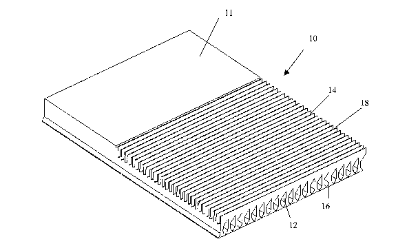
[0020] Figure 1 illustrates one embodiment of a partially-formed surface 10 of
this invention.
The surface 10 includes two sets of channels 12, 14 formed by two sets of fins
16, 18,
respectfully. The surface 10 is preferably, but does not have to be, attached
to a microchip (not
shown) so that the lower set of channels 12 is positioned adjacent to the chip
and runs in a first
direction and the upper set of channels 14 is positioned above the lower set
of channels 12 and
runs in a second direction that is at an angle to the first direction. The
sets of channels 12, 14 are
preferably interconnected to one another by a plurality of passageways 20 (see
Figure 9).
[0021] The surface 10 is preferably formed from a blank of conductive
material, such as
metal (including copper, titanium, aluminum, gold, stainless steel, etc.) and
more preferably
copper. The surface 10 can be formed of any highly-conductive material,
however, such as a
carbide with a high carbon content. Carbon itself could be used to form the
surface 10.
[0022] Figure 1 illustrates a partially-formed surface 10 formed from a blank
11. In a
finished surface 10, fins 16, 18 are preferably, but do not have to be, formed
over the entirety of
the blank 11. To form the surface 10, a lower set of upstanding fins 16 is
fomled on one side of
the blank 11, thereby creating the lower set of channels 12 between the
adjacent fins 16. An
upper set of upstanding fins 18 is then formed on the opposite side of the
blank 11, thereby
creating the upper set of channels 14 between the adjacent fins 18. The sets
of fins 16, 18 may
be formed by many methods known in the art, but preferably are formed by
cutting the sets of
fins 16, 18 and subsequently lifting the sets of fins 16, 18 to a desirable
angle. More specifically,
the sets of fins 16, 18 are formed by cutting layers in the surface of the
blank 11 and lifting the
cut layers to a, desirable angle to fomi upstanding sets of fins 16, 18. This
cutting and lifting
method and a tool for performing this method are disclosed in co-pending
applications US 2004-
0069467 and US 2005-0145377, the entirety of which are hereby incorporated by
reference.
While the sets of fins 16, 18 may be formed on a flat blank, in a preferable
method, the uncut
4
CA 02605966 2007-10-23
WO 2006/133211 PCT/US2006/021959
51aruc is wrappea arouna-a:roraranle drum so that the surface of the blank is
curved in a semi-
circle. In this configuration, the blank emulates a tube surface and
conventional tube surface
enhancement techniques may be used on each side of the blank to form fins 16,
18. It makes no
difference which set of fins 16, 18 (and thus which set of channels 12, 14)
are formed in the
blank first.
[0023] It is preferable, but not necessary, that channels 12, 14 formed by
fins 16, 18 extend
slightly beyond the centerline of the thickness of the blank 11. In this way,
passageways 20 (see
Figure 9) are formed at the intersection of and extend between the upper and
lower set of
channels 12, 14. The portion of channel 12 that extends beyond the centerline
of the blank
intersects with the corresponding portion of channel 14 that extends beyond
the centerline. This
intersection forms a passageway 20 between the two channels 12, 14. Figures 9
and 10 illustrate
the passageways 20. While it is preferable that the channels of both sets of
channels 12, 14
extend beyond the centerline of the blank thickness, the channels of only one
set of channels 12,
14 may so extend to form the passageways 20.
[0024] While the sets of fins 16, 18 (and thus the resulting sets of channels
12, 14) of Figure
1 are shown oriented perpendicular to each other, the sets of fins 16, 18 may
be formed at any
angle relative to each other. Furthermore, the fins within the upper and/or
lower sets of fins 16,
18 (and thus the channels within the upper and/or low sets of channels 12, 14)
need not be
parallel to each other.
[0025] Any number of fins 16, 18 (and thus any number of channels 12, 14) may
be formed
on the cooling surface 10. "Fin pitch" as used herein is defined as the width
of a single channel
plus the thickness of one of the fins defining the channel. The fin pitch of
the upper and lower
sets of fins 16, 18 is preferably, but does not have to be, between 20-1200
fins per inch. The fin
pitch may vary between the lower and upper sets of fins 16, 18 so that the
lower set of fins 16
has a different fin pitch than the upper set of fins 18. Also, the fin pitch
can vary within each set
CA 02605966 2007-10-23
WO 2006/133211 PCT/US2006/021959
or rins i e; '1'~; 'sb 'tn~t ror exampre a portion of the upper set of fins
18 has a different fin pitch
than another portion of the upper set of fins 18.
[0026] Moreover, the height of the fins 16, 18 (and thus the depth of the
upper and lower
channels 12, 14) may also vary between the sets of fins 16, 18 so that the
lower set of fins 16 has
a different fin height than the upper set of fins 18. Similarly, the fin
height can vary within each
set of fins 16, 18, so that for exainple a portion of the upper set of fins 18
has a different fin
height than another portion of the upper set of fins 18.
[0027] The optimal geometries of the sets of fins 16, 18 and the sets of
channels 12, 14 will
depend on a number of factors, including the type of refrigerant used and the
amount of heat
needed to be conducted away from the surface 10. It is preferable, but not
necessary, that the
aspect ratio A for each set of fins 16, 18 (defined as the fin height divided
by the channel width)
be in the range between 0.1< A < 400 and more preferably between 0.1 < A< 40.
[0028] Figure 3 is a cross-sectional view showing the lower set of channels 12
of surface 10
formed by fins 16 having a fin pitch of 100 fins/inch and a fin height of .023
inches. Figure 4 is
a cross-sectional view showing the upper set of channels 14 of surface 10
formed by fins 18
having a fin pitch of 200 fins/inch and a fin height of approximately .0205
inches. Figure 5 is a
cross-sectional view showing the upper set of channels 14 of surface 10 formed
by fins 18
having a fin pitch of 200 fins/inch and a fin height of approximately .0175
inches. Figure 6 is a
cross-sectional view showing the lower set of channels 12 of surface 10 formed
by fins 16
having a fin pitch of 200 fins/inch and a fin height of approximately .021
inches. Figure 7 is a
plan view of the upper set of fins 18 forming channels 14.
[0029] In use, surface 10 is preferably attached to a chip so that the lower
set of channels 12
is proximal the chip. The surface 10 can be attached to the chip in any number
of ways,
including by soldering or using an adhesive or paste. It is preferable that
the adhesive or paste
used be conductive to further facilitate cooling of the chips.
6
CA 02605966 2007-10-23
WO 2006/133211 PCT/US2006/021959
[000] 'b facilitae"a'ttdc'hhient and retention of the surface 10 on and to a
chip, it is
preferable, but not necessary, that the tips of the lower set of fins 16 be
flattened, as shown in
Figures 2, 3, and 6. Such flattening creates additional surface area for
attachment to the chip.
Moreover, the additional surface area provided by flattened tips of the lower
set of fins 16 assists
in the conduction of heat. Figure 8 is a plan view of the lower set of fins 16
forming channels
12. The fins of the lower set of fins 16 have been flattened.
[0031] The tips of the set of fins 16 may be flattened using conventional
flattening
techniques or those described in US 2005-0145377, incorporated herein by
reference. In
addition to flattening, the tips of the set of fins 16 may also be bent over
to form a relatively flat
surface or cut so as to have thickened tips and thus create more surface area
at the tips for
attachment. Methods and tools for bending and thickening fin tips, as well as
angling adjacent
fin tips relative to each other (which is also contemplated by this
invention), are also described in
US 2005-0145377. It is within the scope of the present invention to flatten or
otherwise enhance
the tips of the upper set of fins 18 in addition to or instead of flattening
the tips of the lower set
of fins 16.
[0032] During chip use, a liquid refrigerant is supplied to at least one of
the sets of channels
12, 14. It is preferred that refrigerant is supplied at least to the lower set
of channels 12. Any
number of refrigerants can be used, including but not limited to water or HFE-
71 00, which is
manufactured by 3M. Alternatively, manufacturers such as DuPont or Allied
Signal
manufacture refrigerants known as 134A or 123 that are also appropriate for
use in the current
invention. The refrigerant runs through the lower set of channels 12 to coat
the surface of the
lower set of fins 16. As the lower set of channels 12 becomes filled with the
refrigerant, the
refrigerant is discharged through the passageways 20, and into the upper set
of channels 14 to
coat at least some of the surface of the upper set of fins 18. In another
embodiment, refrigerant
7
CA 02605966 2007-10-23
WO 2006/133211 PCT/US2006/021959
njay e'e st~p'p'li~d"CtireCCl~"'to"trie upper set of channels 14 instead of or
in addition to supplying
refrigerant to the lower set of channels 12.
[0033] The heat generated by the chip is transferred to the conductive surface
10. By virtue
of this heat transfer, the temperature of the liquid refrigerant in channels
12, 14 elevates,
converting at least some of the liquid refrigerant to vapor. At least some of
the vapor produced
in the lower set of channels 12 is discharged through passageways 20 and into
the upper set of
channels 14, thereby carrying heat away from the chip. Moreover, as the
refrigerant that is not
vaporized flows through and exits the sets of channels 12, 14, heat generated
by the chip is
carried away in that refrigerant. In this way, heat generated by the chip is
carried away by the
refrigerant, either in liquid or vapor form.
[0034] A puinp (not shown) can be used to pump the liquid refrigerant into one
or both of the
channels 12, 14 and thereby prevent all of the refrigerant from vaporizing.
Rather, while some
of the refrigerant will turn to vapor during the heat transfer process, the
pump replenishes the
refrigerant to the cooling surface 10 so that a combination of liquid
refrigerant and vapor is
present in the sets of channels 12, 14. The pump can continuously supply
refrigerant to the sets
of channels 12, 14. Alternatively, a controller for the pump may be used to
monitor the
temperature of the chip and activate the pump only when the temperature
increases to a
predetermined amount.
[0035] Supplying refrigerant to the sets of channels 12, 14 (either
continuously or with a
sensor) ensures that the sets of fins 16, 18 remain coated with refrigerant.
It is desirable that
only a thin film of the refrigerant coat the sets of fins 16, 18. The heat
transfer coefficient is a
measure of how effectively heat is transferred away from the chip - a higher
heat transfer
coefficient ensures that heat is more effectively transferred away. A thin
film of refrigerant is
preferred because the heat transfer coefficient is inversely proportional to
the thickness of the
refrigerant layer on the sets of fins 16, 18. Accordingly, a thin film of
refrigerant ensures a high
8
CA 02605966 2007-10-23
WO 2006/133211 PCT/US2006/021959
hbdt trftnS'ter tO)~~ttitidht;"Ciiereby"improving the ability of the cooling
surface 10 to transfer heat
away from the chip.
[0036] Provision of two sets of channels 12, 14 formed by two sets of fins 16,
18 in cooling
surface 10 is particularly beneficial in this application. By forming two sets
of fins 16, 18, the
fin height of the surface 10 and consequently the surface area available for
contact with the
refrigerant is essentially doubled, as compared to a cooling surface that has
only a single set of
channels and fins. The increased surface area allows more heat to be conducted
into the
refrigerant and away from the chip.
[0037] Figures 1 and 9 illustrate surfaces 10 where the upper set of fins 18
and channels 14
are formed at substantially 90 relative to the lower set of fins 16 and
channels 12. As explained
above, however, the upper and lower sets of fins and channels need not be
oriented 90 relative
to each other. Rather, the upper and lower sets of fins and channels may be
formed at acute
angles relative to each other, as shown in Figure 10.
[0038] In one embodiment of the current invention, the cooling surface 10 can
be stretched
after the cooling surface 10 is formed. Stretching is particularly suitable
with surfaces 10 having
set of fins 16, 18 and channels 12, 14 oriented at acute angles relative to
each other. Stretching
leads to manufacturing conveniences. As opposed to manufacturing a variety of
cooling surfaces
each with characteristics (fin height, pitch, etc.) intended for a specific
application, a single
cooling surface 10 may be manufactured and then stretched to tailor the
surface to a particular
application. For example, stretching the cooling surface 10 can increase the
fin pitch or alter the
aspect ratio. Moreover, as explained above, all of the fins in a set of fins
16, 18 need not have
the same fin pitch or fin count and indeed it may be desirable that they do
not. Stretching the
cooling surface 10 allows selective variation of the fin characteristics
within a set of fins 16, 18
to better tailor the cooling surface 10 to a particular application and thus
enhance the
effectiveness of the cooling surface 10. Figure 10 illustrates a partially-
stretched cooling surface
9
CA 02605966 2007-10-23
WO 2006/133211 PCT/US2006/021959
l'bl'-,-'The pbt=tr6rY 'bf''tTie"gUY"radeT'U-'Yn the lower left hand corner of
Figure 10 has been stretched to
a lesser degree than the remaining portions of the surface 10.
[0039] The foregoing is provided for the purpose of illustrating, explaining
and describing
embodiments of the present invention. Further modifications and adaptations to
these
embodiments will be apparent to those skilled in the art and may be made
witliout departing
from the spirit of the invention or the scope of the claims.