Note: Descriptions are shown in the official language in which they were submitted.
CA 02606893 2007-10-15
TUNING AN RFID READER WITH ELECTRONIC SWITCHES
TECHNICAL FIELD
The present invention relates generally to RFID systems, particularly to the
construction and operation of a reader and associated transponder in an RFID
system,
and more particularly to the construction and operation of a reader having
adjustable
tuning capacitance to enhance the range of the reader for communication with
the
transponder.
BACKGROUND OF THE INVENTION
Radio frequency identification (RFID) systems typically include at least one
reader and a plurality of transponders, which are commonly termed credentials,
cards,
tags, or the like. The transponder may be an active or passive radio frequency
communication device which is directly attached to or embedded in an article
to be
identified or otherwise characterized by the. reader. Alternatively, the
transponder may
be embedded in a portable substrate, such as a card or tag, carried by a
person to be
identified or otherwise characterized by the reader. An active transponder is
powered
up by its own intemal power supply, such as a battery, which provides the
operating
power for the transponder circuitry. In contrast, a passive transponder is
characterized
as being dependent on the reader for its power. The reader "excites" or powers
up the
passive transponder by transmitting excitation signals of a given frequency
into the
space surrounding the reader, which are received by the transponder and
provide the
operating power for the circuitry of the recipient transponder.
Communication between the reader and transponder is enabled by cooperative
resonant circuits which are provided in each reader and transponder. The
resonant
circuit of a reader typically includes an inductor and a capacitor. The
capacitor is
coupled in series between the inductor and a signal driver. The inductor is
usually in
the form of an antenna coil which is capable of magnetically coupling to an
inductor in
the resonant circuit of a compatible transponder through mutual inductance.
1
CA 02606893 2007-10-15
Communication is initiated when a transponder is proximally positioned
relative to the
reader. The reader has a power supply which conveys a current to the reader
resonant
circuit causing the reader antenna to produce an excitation signal in the form
of an
electromagnetic field. The excitation signal couples to the antenna of the
proximally-
positioned transponderthrough mutual inductance and the excitation signal
powers and
clocks the transponder circuitry initiating operation of the transponder.
Transponder operation comprises generation of a response signal at a specified
frequency and transmission of the resulting transponder response signal back
to the
reader. In particular, the transponder resonant circuit receives a current in
response
to the excitation signal which causes the transponder antenna to produce a
response
signal in the form of an electromagnetic field. The response signal couples to
the
reader antenna through mutual inductance in substantially the same manner as
described above with respect to coupling of the excitation signal to the
transponder
antenna.
The transponder modulates the response signal to encode data stored in the
memory of the transponder circuitry into the response signal. When the
response
signal couples to the reader antenna, a corresponding voltage is induced in
the reader
antenna at the specified frequency. The reader processes the induced voltage
to read
the data encoded in the response signal. The resulting data_may be
communicated to
an output device, such as a display, printer, or storage device, and
simultaneously, or
alternatively, communicated to a host computer, if a host computer is
networked into
the RFID system.
An important operating parameter of the reader is the range of the reader when
communicating with a transponder. The range of the reader is inter alia
strongly
affected by the strength of the electromagnetic field generated by the reader
resonant
circuit. In order to generate a field strength which provides the reader with
adequate
range, the designer of the reader must properly specify a resonant circuit
which is
appropriately tuned to a predetermined frequency for the desired application
of the
RFID system.
The range of the reader is often altered by the characteristics of the
operating
2
CA 02606893 2007-10-15
environment in which the reader resides. In a typical case where the reader is
mounted
in a fixed location on a support structure, the range of the reader is
susceptible to the
materials of the mounting location and other objects within the operating
environment.
For example, if the mounting location of the reader is in an operating
environment
which includes nearby metal, the metal can detune the resonant circuit of the
reader
from the predetermined frequency and dramatically reduce the range of the
reader.
The presence of one or more transponders in the operating environment of the
reader
which have variations in their respective resonant circuits due to . imprecise
manufacturing tolerances can detune the resonant circuit of the reader.
Imprecise
manufacturing tolerances in the resonant circuit of the reader can also detune
the
resonant circuit of the reader.
One means of overcoming the above-mentioned problems is to provide the
reader resonant circuit with an adjustable tuning capability so that the
tuning of the
reader resonant circuit is adjusted in response to variations in its operating
environment. As such, the present invention recognizes a need for a reader of
an RFID
system which is adaptable to variations in its operating environment.
Accordingly, it is
generally an object of the present invention to provide an RFID system having
a reader
which exhibits satisfactory performance characteristics while adjusting to
variations in
a given system operating environment. More particularly, it is an object of
the present
invention to provide a reader achieving a uniformly satisfactory level of
performance
when the reader is employed in different operating environments. It is another
object
of the present invention to provide a reader having a resonant circuit which
automatically retunes itself to maintain a desired performance level in
response to
variations in the operating environment of the reader. These objects and
others are
accomplished in accordance with the invention described hereafter.
SUMMARY OF THE INVENTION
The present invention is a reader for an RFID system comprising a signal
driver
for generating an excitation signal and a resonant circuit having an
adjustable resonant
3
CA 02606893 2007-10-15
circuit capacitance for retuning the resonant circuit in response to detuning.
The
resonant circuit includes a capacitance tuning circuit and a transmitting
antenna
coupled with the capacitance tuning circuit for transmitting the excitation
signal having
a carrier frequency into a space surrounding the transmitting antenna. The
capacitance
tuning circuit includes a fine-tuning capacitor having a fine-tuning
capacitance and a
fine-tuning capacitor switch having an open position and a closed position.
The fine-
tuning capacitance is added to the adjustable resonant circuit capacitance
when the
fine-tuning capacitor switch is in the closed position and is removed from the
adjustable
resonant circuit capacitance when the fine-tuning capacitor switch is in the
open
position.
In another characterization of the invention, the capacitance tuning circuit
includes a first fine-tuning capacitor having a first fine-tuning capacitance,
a first fine-
tuning capacitor switch having an open position and a closed position, a
second fine-
tuning capacitor having a second fine-tuning capacitance and a second fine-
tuning
capacitor switch having an open position and a closed position. The first fine-
tuning
capacitance is added to the adjustable resonant circuit capacitance when the
first fine-
tuning capacitor switch is in the closed position and is removed from the
adjustable
resonant circuit capacitance when the first fine-tuning capacitor switch is in
the open
position. The second fine-tuning capacitance is added to the adjustable
resonant
circuit capacitance when the second fine-tuning capacitor switch is in the
closed
position and is removed from the adjustable resonant circuit capacitance when
the first
fine-tuning capacitor switch is in the open position.
The capacitance tuning circuit preferably further includes a carrier frequency
capacitor having a carrier frequency capacitance. The carrier frequency
capacitance
is added to the resonant frequency capacitance and the carrier frequency
capacitor
sets the carrier frequency of the excitation signal in cooperation with the
transmitting
antenna.
In another characterization of the invention, the capacitance tuning circuit
includes a first carrier frequency capacitor having a first carrier frequency
capacitance,
a first carrier frequency capacitor switch having an open position and a
closed position,
4
CA 02606893 2007-10-15
a second carrier frequency capacitor having a second carrier frequency
capacitance
and a second carrier frequency capacitor switch having an open position and a
closed
position. A first excitation signal having a first carrier frequency is
transmitted from the
transmitting antenna when the first carrier frequency capacitor switch is in
the closed
position and the second carrier frequency capacitor switch is in the open
position. A
second excitation signal having a second carrier frequency is transmitted from
the
transmitting antenna when the first carrier frequency capacitor switch is in
the open
position and the second carrier frequency capacitor switch is in the closed
position.
The present invention is also a method for tuning a reader for an RFID system.
An excitation signal is generated in a signal driver. The excitation signal is
conveyed
to a resonant circuit having a capacitance tuning circuit and a transmitting
antenna
coupled with the capacitance tuning circuit. The excitation signal having a
carrier
frequency is transmitted into a space surrounding the transmitting antenna in
the form
of a magnetic field having a field strength. The resonant circuit is retuned
to the carrier
frequency in response to detuning by transitioning a fine-tuning capacitor
switch from
an open position to a closed position to add a fine-tuning capacitance of a
fine-tuning.
capacitor coupled with the fine-tuning capacitor switch into the resonant
circuit or by
transitioning the fine-tuning capacitor switch from a closed position to an
open position
to remove the fine-tuning capacitance of the fine-tuning capacitor from the
resonant.
circuit.
The present invention will be further understood from the drawings and the
following detailed description.
BRIEF DESCRIPTION OF THE DRAWINGS
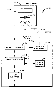
Figure 1 is a block diagram of an RFID system employing a reader.
Figure 2 is a schematic view of a reader signal generator including a
capacitance
tuning circuit having utility in the reader of Figure 1.
Figure 3 is a schematic view of a solid-state relay switch employed in the
capacitance tuning circuit of Figure 2.
5
CA 02606893 2007-10-15
Figure 4 is a schematic view of a reader signal generator including a pair of
capacitance tuning circuits having utility in the reader of Figure 1.
Embodiments of the invention are illustrated by way of example and not by way
of limitation in the above-recited figures of the drawings, wherein like
reference
characters indicate the same or similar elements. It should be noted that
common
references= to "an embodiment", "one embodiment", "an alternate embodiment",
"a
preferred embodiment", or the like herein are not necessarily references to
the same
embodiment.
DESCRIPTION OF PREFERRED EMBODIMENTS
Referring initially to Figure 1, a conceptualized embodiment of an RFID system
is shown and generally designated 10. The RFID system 10 comprises a
transponder
12 and a reader 14. The transponder 12 is preferably a passive device, which
is not
physically coupled with an electrical power supply. The electrical power
required to
operate the transponder 12 is indirectly supplied to the transponder 12 by
electromagnetic waves, which are periodicaily propagated through open space 16
to
the transponder 12 from the reader 14. The transponder 12 is only operational
when
it is receiving electromagnetic waves from the reader 14 of a specific
frequency and of
sufficient strength to power up the transponder 12.
The transponder 12 includes a transponder integrated circuit (IC) 18 and a
transponder antenna 20 coupled with the transponder IC 18. The transponder
antenna
20 is a single conventional coil which performs both the receiving and
transmitting
functions of the transponder 12. Thus, the transponder antenna 20 is termed a
"dual-
function antenna." However, the present invention is not limited to an RFID
system
having a transponder with a single dual-function transponder antenna. The
present
invention alternately encompasses an RFID system having a transponder with
separate
receiving and transmitting antennas, which separately perform the receiving
and
transmitting functions of the transponder.
The transponder IC 18 is preferably a custom IC which satisfies essentially
all
6
CA 02606893 2007-10-15
remaining required transponder functionalities, such as disclosed in U.S.
Patents
4,730,188 to Milheiser (the '188 Patent) and 5,541,574 to Lowe et al. (the
'574 Patent),
which are incorporated herein by reference. The transponder 12 optionally, but
preferably, includes a transponder tuning capacitor 22 coupled with the
transponder IC
18 and transponder antenna 20. The transponder antenna 20, in association with
the
transponder tuning capacitor 22, if present, define the transponder resonant
circuit.
The carrier frequency of the transponder 12 is determined by selecting an
antenna and
optionally a tuning capacitor for the transponder 12 tuned to the carrier
frequency,
which is typically either 125 kHz or 13.56 MHz.
It is understood that the present invention is not limited to any one specific
type
of transponder, but is generally applicable to most conventional types of
transponders
having utility in RFID systems. Thus, for example, the transponder 12 can be
selected
from proximity cards, proximity tags, smart cards, or the like. It is further
understood
that the RFID system 10 is not limited to RFID systems having only one
transponder
and one reader as shown. The present RFID system 10 is shown as such primarily
for
ease of description. In practice, RFID systems having utility in the present
invention
typically include any number of compatible transponders and can also include a
plurality of compatible readers.
The reader 14 comprises a reader signal generator 24, reader receiver
electronics 26, a reader microcontroller 28, a reader input/output (I/O)
interface 30, a
reader power supply 32, and a reader antenna 34. The reader power supply 32 is
a
finite electrical power source which is self-contained (i.e., internal) within
the reader 14,
such as a relatively small portable battery consisting of one or more
disposable dry cells
or rechargeable cells. Alternatively, the reader 14 is operable with a power
supply
which is hard wired to an essentially infinite remote electrical power source,
such as an
electric utility.
The reader signal generator 24 is coupled with the reader microcontroller. 28
for
generating relatively low energy electromagnetic waves termed "ring signals"
or
"detection signals" and for generating relatively high energy electromagnetic
waves
termed "excitation signals" under the direction of the reader microcontroller
28. The
7
CA 02606893 2007-10-15
reader signal generator 24 is also coupled with the reader antenna 34 for
transmitting
the detection and excitation signals from the reader 14 through the open space
16 for
reception by any-nearby transponders which are tuned to the same frequency as
the
reader 14.
The detection and excitation signals transmitted from the reader 14 typically
have a limited range due to size and power constraints of the reader 14. Thus,
the
reader 14 and transponder 12 of the RFID system 10 are simultaneously
operational
only when the transponder 12 is within the range of the reader 14 and, more
particularly, when the reader 14 and transponder 12 are positioned in relative
proximity
to one another such that the transponder 12 receives excitation signals of
sufficient
strength and an appropriate frequency from the reader 14 to power up the
transponder
12.
In most conventional RFID systems, the position of the reader is stationary
(i.e.,
constant) relative to the surrounding environment, while the position of the
transponder
is portable (i.e., variable) within the surrounding environment. In such
cases, the user
of the RFID system moves the portable transponder into relative, proximity
with the
stationary reader to enable simultaneous operation of the both the transponder
and
reader. In some conventional RFID systems, however, the position of the reader
may
be portable relative to the surrounding environment, while the position of the
transponder is either portable or stationary. In the case of a portable reader
and a
stationary transponder, the user moves the portable reader into relative
proximity with
the stationary transponder to enable simultaneous operation of the both Ahe
transponder and reader. In the case of a portable reader and a portable
transponder,
the user may move both the portable reader and the portable transponder into
relative
proximity with one another to enable simultaneous operation of the both the
transponder and reader. The present invention is not limited to any one of the
above-
recited RFID system configurations.
The reader signal generator 24 initially operates in a transponder detection
mode
under the direction of the reader microcontroller 28. The transponder
detection mode
is a reduced power state of operation which is effected by periodically
drawing reduced
8
CA 02606893 2007-10-15
electrical current from the reader power supply 32 to the reader signal
generator 24
which periodically generates detection signals containing analog data in
response to
the reduced electrical current. The detection signals, which are of
insufficient strength
to power operation of any transponders 12 residing in the open space 16
surrounding
the reader 14, are periodically transmitted from the reader 14 and propagate
into the
open space 16. Propagated detection signals returned to the reader 14 via the
reader
antenna 34 are monitored and evaluated by the reader 14 when operating in the
transponder detection mode.
The monitoring and evaluating functionalities are integrated into the reader
microcontroller 28, which is preferably a single-chip device. The reader
receiver
electronics 26, like the reader signal generator 24, are coupled with the
reader
microcontroller 28 as well as with the reader antenna 34. Figure 1 shows an
embodiment of the reader circuitry where one end of the reader antenna. 34 is
coupled
with the reader signal generator 24, while coupling the reader receiver
electronics 26
with the other end of the reader antenna 34. It is alternately within the
purview of the
skilled artisan to couple the reader signal generator 24 and reader receiver
electronics
26 with the same end of the reader antenna 34, thereby driving and receiving
signals
at the same end of the reader antenna 34. It is further within the scope of
the present
invention to couple the reader signal generator 24 with both ends of the
reader antenna
34, while coupling the reader receiver electronics 26 with either one or both
ends of the
reader antenna 34. The present invention is not limited to any one of the
above-recited
antenna coupling configurations.
The transponder detection mode functionalities are enabled at least in part by
specific software and/orfirmware included in the reader microcontroller 28.
The reader
microcontroller 28 converts the analog data of the detection signals to
digital data and
identifies changes in degree and/or changes in kind within the digital data
and further
recognizes which changes in the digital data correspond to changes in one or
more
selected detection parameters, such as the decay rate or voltage of the
detection
signals. Changes in one or more of the selected detection parameters indicates
the
presence of a transponder 12 having a given frequency in the open space 16.
9
CA 02606893 2007-10-15
When the reader microcontroller 28 detects a transponder 12, it switches the
reader signal generator 24 from the transponder detection mode to a
transponder
excitation mode at an increased power state of operation. Switching the reader
signal
generator 24 to the excitation mode terminates periodic generation of the
detection
signals of the given frequency and causes the reader signal generator 24 to
draw
increased electrical current from the reader power supply 32. The increased
draw of
electrical current in the excitation mode enables the reader signal generator
24 to
generate an excitation signal of the given frequency under the direction of
the reader
microcontroller 28. The excitation signal is in the form of an electromagnetic
wave,
which has sufficient strength to power up the transponder 12. When the
transponder
12 and/or reader 14 is moved to a proximal position such that the distance
between
reader 14 and transponder 12 is within the excitation signal reception range
of the
transponder antenna 20, the transponder antenna 20 receives the excitation
signal at
a sufficient strength to power up the transponder IC 18, thereby activating
the
transponder 12.
Upon activation, the transponder IC 18 generates a communication signal
termed a transponder data signal, which contains readable information (i.e.,
digital
data) copied or otherwise derived from the memory of the transponder IC 18.
The
transponder data signal is in the form of an electromagnetic wave like the
excitation
signal. The transponder 12 transmits the transponder data signal into the open
space
16 of the external environment via the transponder antenna 20. .
The reader antenna 34 as shown is a conventional coil acting as a single dual-
function antenna, which performs both the receiving and transmitting functions
of the
reader 14. In particular, the reader antenna 34 receives the detection signals
and the
transponder data signals from the open space 16 and transmits the detection
and
excitation signals into the open space 16. However, the present invention is
not limited
to an RFID system having a reader with dual-function antennas. The present
invention
alternately encompasses an RFID system having a reader with separate receiving
and
transmitting antennas, which separately perform the transponder data signal
and
detection signal receiving functions of the reader and the detection signal
and excitation
CA 02606893 2007-10-15
signal transmitting functions of the reader, respectively. In yet another
altemative,
where a reader is provided with separate receiving and transmitting antennas,
the
reader transmitting antennas are capable of being adapted to act as dual-
function
antennas (i.e., receiving and transmitting) only with respect to the detection
signals
while the reader transmitting and receiving antennas function separately with
respect
to the transponder data signals.
Transponder data signal reading components and their corresponding
functionality are integrated into the reader microcontroller 28 along with the
transponder
detection components and the components for activating the excitation mode and
their
corresponding functionalities described above. The transponder data signal
reading
functionalities are enabled in part by specific firmware included in the
reader
microcontroller 28. The receiver electronics 26 receive the transponder data
signals
for any of a plurality of data rates and modulation types, from the reader
antenna 34
and "condition" the transponder data signals. The reader microcontroller 28
demodulates the conditioned transponder data signals in accordance with the
respective modulation type of the signal to read the data on the signals. The
resulting
data can then be sent to an external device (not shown), such as a central
host
computer, via the reader I/O interface 30.
The reader signal generator 24 of the present invention is more particularly
characterized as having a capacitance tuning circuit employing one or more
capacitors
and associated switches described hereafter. The capacitance tuning circuit is
coupled
with the reader antenna 34 and, in combination with the reader antenna 34,
defines a
reader resonant circuit having a tunable resonant frequency (i.e., tunable
carrier
frequency). A specific embodiment of a reader signal generator 24 having a
capacitance tuning circuit 36 is shown and described hereafter with reference
to Figure
2. The capacitance tuning circuit 36 comprises a first parallel (or shunt)
capacitor 38
having an associated first parallel (or shunt) capacitor switch 40, a second
parallel (or
shunt) capacitor 42 having an associated second parallel (or shunt) capacitor
switch
44, a first series capacitor 45 having an associated first series capacitor
switch 46, a
second series capacitor 47 having an associated second series capacitor switch
48,
11
CA 02606893 2007-10-15
and a third series capacitor 49 having an associated third series capacitor
switch 50.
The reader signal generator 24 further comprises an AC signal source 54 and
signal driver 56 which are functionally and structurally similar to those
disclosed in the
'188 and '574 Patents. The AC signal source 54 and signal driver 56 are
coupled in
series with the capacitance tuning circuit 36, which is in turn coupled with
the reader
antenna 34. The reader antenna 34 in combination with the capacitance tuning
circuit
36 are the reader resonant circuit 58. More particularly, the first, second
and third
series capacitors 45, 47, 49 are positioned upstream of the first and second
parallel
capacitors 38,42 coupled between the signal driver 56 and the first and second
parallel
capacitors 38, 42. The first and second series capacitors 45, 47 are
individually
positioned in parallel relative to one another. The first and second parallel
capacitors
38, 42 are coupled between the first and second series capacitors 45, 47 and
the
reader antenna 34. The first and second parallel capacitors '38, 42 are
likewise
individually'positioned in parallel relative to one another.
Each capacitor switch 40, 44, 46, 48, 50 has an open position and a closed
position and is selectively transitionable between the open position and the
closed
position under the control of a switch controller. When the first parallel
capacitor switch
40 is in the closed position, it switches the entire capacitance of the first
parallel
capacitor 38 into the reader resonant circuit 58, thereby increasing the
capacitance of
the reader resonant circuit 58 in identical correspondence with the
capacitance of the
first parallel capacitor 38 (assuming a perfect or ideal switch). Similarly,
when any of
the remaining switches 44, 46, 48, or 50 is in the closbd position, it
switches the entire
capacitance of the associated capacitor 42, 45, 47, or 49 into the reader
resonant
circuit 58, thereby increasing the capacitance of the reader resonant circuit
58 in
identical correspondence with the capacitance of the associated capacitor 42,
45, 47,
or 49 (assuming a perfect or ideal switch).
Conversely, when the first parallel capacitor switch 40 is in the open
position, it
switches the entire capacitance of the first parallel capacitor 38 out of the
reader
resonant circuit, thereby decreasing the capacitance of the reader resonant
circuit 58
in identical correspondence with the capacitance of the first parallel
capacitor 38
12
CA 02606893 2007-10-15
(assuming a perfect or ideal switch). Similarly, when any of the remaining
switches 44,
46, 48, or 50 is in the open position, it switches the entire capacitance of
the associated
capacitor 42, 45, 47, or 49 out of the reader resonant circuit 58, thereby
decreasing the
capacitance of the reader resonant circuit 58 in identical correspondence with
the
capacitance of the associated capacitor 42, 45, 47, or 49 (assuming a perfect
or ideal
switch). Thus, for example, if a capacitor has a capacitance of 10 picofarads,
a perfect
associated capacitor switch would switch 10 picofarads into the resonant
circuit 58
when in a closed position, but would switch 0 picofarads into the resonant
circuit 58
when in an open position.
The capacitance tuning circuit 36 is commonly operated in a manner which
maintains the strength of the magnetic field generated by the reader resonant
circuit
58 at the reader antenna 34 at a maximum level for a given amount of voltage
supplied
to the reader resonant circuit 58, thereby maximizing the range of the reader
14. More
particularly, the capacitance tuning circuit 36 is operated in accordance with
the present
invention such that the strength of the magnetic field generated by the reader
resonant
circuit 58 at the reader antenna 34 is maintained at a maximum level for a
given
amount of voltage in substantially all common operating cases, i.e., when no
transponder is present in the range of the reader 14, when a single
transponder is
present in the range of the reader, or when multiple transponders are present
in the
range of the reader 14.
As a general rule, the magnetic field strength generated by the reader
resonant
circuit 58 and correspondingly the range of the reader 14 are both directly
correlated
to the inductance of the reader antenna 34. Accordingly, a reduction in the
inductance
of the reader antenna 34 for any reason undesirably alters the resonant
frequency of
the reader resonant circuit 58, which in tum decreases the magnetic field
strength
generated by the reader resonant circuit 58 and correspondingly decreases the
range
of the reader 14.
It has been found, however, that the above-recited undesirable effects, which
occur when the inductance of the reader antenna 34 decreases, can be offset by
increasing the capacitance of the reader resonant circuit 58. Accordingly, the
13
CA 02606893 2007-10-15
practitioner increases the capacitance of the reader resonant circuit 58 in
response to
a decrease in the inductance of the reader antenna 34 in order to maintain a
given
resonant frequency, i.e., carrier frequency, thereby maintaining the magnetic
field
strength at the reader antenna 34 at or near a desired maximum during
operation of the
reader 14.
Detuning of the reader resonant circuit 58 can occur when aberrant
environmental conditions, such as a proliferation of metal objects in the
surrounding
environment of the reader 14, decrease the effective inductance of the reader
antenna
34. In general, the reader resonant circuit 58 is preferably retuned in
response to such
detuning by transitioning one or more capacitor switches in the capacitance
tuning
circuit 36 from an open position to a closed position or from a closed
position to an
open position, thereby adding or removing the capacitance contribution of the
respective associated capacitor to or from the total capacitance of the reader
resonant
circuit 58.
In accordance with one embodiment, the reader antenna 34 is more particularly
characterized as a dual-function, single frequency antenna because it performs
both
the receiving and transmitting functions of the reader resonant circuit 58,
but only for
a specific resonant frequency, i.e., typically either 125 kHz or 13.56 MHz..
The first
series capacitor 45 is more particularly characterized as a carrier frequency
capacitor
because it is selected by the designer of the capacitance tuning circuit 36
such that the
first series capacitor 45, in cooperation with the reader antenna 34, sets the
desired
carrier frequency of the reader resonant circuit 58 subject to retuning in a
manner
described below. The second and third series capacitors 47, 49 and the first
and
second parallel capacitors 38, 42 are more particularly characterized as fine-
tuning
capacitors because they are selected by the designer of the capacitance tuning
circuit
36 such that the capacitors 38, 42, 47, 49 in cooperation with their
associated switches
40, 44, 48, 50, enable retuning of the reader resonant circuit 58 to restore
the desired
carrier frequency in response to detuning.
The design capacitances of the fine-tuning capacitors 38, 42, 47, 49 are
preferably different from one another and are each preferably substantially
less than
14
CA 02606893 2007-10-15
the design capacitance of the carrier frequency capacitor 45. For example, the
first
series capacitor 45 may have a relatively high design capacitance to effect a
resonant
frequency of 125 kHz in the reader resonant circuit 58, while the fine-tuning
capacitors
38, 42, 47, 49 have a relatively low design capacitance, thereby effecting
only a
relatively small tuning variance in the reader resonant circuit 58.
The present invention encompasses substantially any initial configuration of
the
capacitor switch positions in the reader resonant circuit 58 as long as at
least the
capacitor switch associated with the carrier frequency capacitor is in the
closed
position. For example, the capacitor switches of the reader resonant circuit
58 may be
initially configured such that only the first series capacitor switch 46 is in
an initial closed
position while the remaining fine-tuning capacitor switches 40, 44, 48, 50 are
in an
initial open position. Accordingly, only the first series capacitor 45
contributes to the
total capacitance of the reader resonant circuit 58 during initial operation
of the reader
14, while none of the remaining fine-tuning capacitors 38, 42, 47, 49
contribute to the
total capacitance of the reader resonant circuit 58 during initial operation.
If the reader
resonant circuit 58 becomes detuned during reader operation by a decrease in
effective
inductance due to certain environmental factors, the capacitance tuning
circuit 36
transitions one, all, or any combination of the fine-tuning capacitor switches
40, 44, 48,
50 from the open position to the closed position to increase the capacitance
of the
reader resonant circuit 58 in correspondence with the capacitances of the one
or more
fine-tuning capacitors associated with the one or more closed fine-tuning
capacitor
switches. The particular one or more fine-tuning capacitor switches which are
transitioned from the open to the closed position is a function of the level
of increased
capacitance needed. In any case, the resulting increased capacitance retunes
the
reader resonant circuit 58 to the desired carrier frequency and desirably
maximizes the
magnetic field strength at the reader antenna 34.
In some cases, it may be desirable to either increase or decrease the total
capacitance of the reader resonant circuit 58 such as in certain cases where
the reader
resonant circuit 58 becomes detuned as a result of manufacturing variations in
the
reader resonant circuit 58 or in the resonant circuit of an associated
transponder 12.
CA 02606893 2007-10-15
In accordance with an alternate exemplary initial switch position
configuration, which
may apply to such cases, the reader resonant circuit 58 initially maintains
the first
series capacitor switch 46 in the closed position as in the above-recited
exemplary
switch position configuration. In accordance with the present configuration,
however,
the reader resonant circuit 58 also preferably initially maintains one or more
of the
remaining fine-tuning capacitor switches 40, 44, 48, 50 in the closed
position.
Accordingly, the carrier frequency capacitor and fine-tuning capacitors having
associated capacitor switches in the initial closed position contribute to the
total
capacitance of the reader resonant circuit 58 during initial operation of the
reader 14,
while none of the remaining capacitors having associated capacitor switches in
the
initial open position contribute to the total capacitance of the reader
resonant circuit 58.
If it is desired to decrease the capacitance of the reader resonant circuit 58
during reader operation, the capacitance tuning circuit 36 transitions one or
more of the
fine-tuning capacitor switches from the closed position to the open position
depending
on which of the one or more fine-tuning capacitor switches is in the initial
closed
position and depending on the desired level of decreased capacitance.
Transitioning
the fine-tuning capacitor switch from the closed position to the open position
removes
the capacitance contribution of the fine-tuning capacitor associated with the
open
switch from the total capacitance of the reader resonant circuit 58 for
further operation
of the reader 14.
It is apparent from the above, that the reader resonant circuit 58 can be
retuned
from substantially any initial or subsequent switch position configuration by
selectively
transitioning the fine-tuning capacitor switches between the open and closed
positions
to selectively add or remove the capacitance contribution of the respective
associated
fine-tuning capacitor. In a preferred embodiment, the reader microcontroller
28
preferably automatically sets the initial positions of the capacitor switches
40, 44, 46,
48, 50 in the capacitance tuning circuit 36. The reader microcontroller 28
subsequently
automatically detects any detuning of the reader resonant circuit 58 and
automatically
controls transitioning of the switch positions in the manner recited above to
retune the
reader resonant circuit 58 and restore optimal operation of the reader 14.
Accordingly,
16
CA 02606893 2007-10-15
the resonant circuit 58 of the reader 14 is essentially self-tuning without
requiring
substantial user input.
In accordance with another embodiment, the reader antenna 34 is more
particularly characterized as a dual-function, dual-frequency antenna because
it
performs both the receiving and transmitting functions of the reader resonant
circuit 58
for two different selectable resonant frequencies. As in the above-recited
embodiment,
the first series capacitor 45 is characterized as a carrierfrequency
capacitor, and more
particularly a first carrier frequency capacitor, because the first series
capacitor 45, in
cooperation with the reader antenna 34, sets a first selectable resonant
frequency of
the reader resonant circuit 58, e.g., 125 kHz. However, the second series
capacitor 47
is also characterized as a carrier frequency capacitor, and more particularly
a second
carrier frequency capacitor, because when selectively operational to the
exclusion of
the first series capacitor 45 in a manner described below the second series
capacitor
47, in cooperation with the reader antenna 34, sets a second selectable
resonant
frequency of the reader resonant circuit 58, e.g., 13.56 MHz. The third series
capacitor
49 and first and second parallel capacitors 38, 42 remain fine-tuning
capacitors as in
the above-recited embodiment.
The capacitor switches of the reader resonant circuit 58 in the present
embodiment are initially configured such that either the first or the second
series
capacitor switch 46, 48 is in an initial closed position while the other
series capacitor
switch is in an initial open position. The choice of which series capacitor
switch is
maintained in the closed position and which series capacitor switch is
maintained in the
open position depends on the desired carrier frequency of reader operation.
For
example, maintaining the first series capacitor switch 46 in the closed
position and the
second series capacitor switch 48 in the open position may effect a resonant
frequency
of 125 kHz in the reader resonant circuit 58. Conversely, maintaining the
first series
capacitor switch 46 in the open position and the second series capacitor
switch 48 in
the closed position may effect a resonant frequency of 13.56 MHz in the reader
resonant circuit 58.
Once the initial positions of the first and second series capacitor switches
46, 48
17
CA 02606893 2007-10-15
are selected, the initial switch position configuration and operation of the
remaining
fine-tuning switches 40, 44, 50 is performed in substantially the same manner
as
described above to enable retuning of the reader resonant circuit 58 to
whichever
carrier frequency is selected at that time.
Each capacitor switch 40, 44, 46, 48, 50 of the capacitive tuning circuit 36
can
be any one of a number of structural altematives. In accordance with one
alternative,
each capacitor switch 40, 44, 46, 48, 50 is a mechanical switch having a
manual switch
control function. As such, the switch controller is in the form of a manually
operated
jumper, lever, push button, rotatable knob, slider, or the like.
Alternatively, each
capacitor switch 40, 44, 46, 48, 50 is a solenoid relay switch having an
automated
electronic switch control function. As such, the switch controller is
preferably a
microcontroller which may be functionally integrated into the reader
microcontroller 28,
in which case the switch controller is likewise structurally subsumed by the
reader
microcontroller 28. Although control of a solenoid relay switch is preferably
effected
electronically, the actual switch action is mechanical. A disadvantage of this
is that the
mechanical motion can cause the switch contacts to wear out over time.
Solenoid relay
switches also tend to be relatively large and are relatively noisy during
operation.
A more preferred altemative capacitor switch 40, 44, 46, 48, 50 is a solid-
state
relay switch including a transistor. More specifically, the transistor is
preferably a field
effect transistor (FET), more specifically still, the transistor is preferably
a metal oxide
semiconductorfield effect transistor (MOSFET), and more specifically yet, the
transistor
is preferably a power MOSFET. The switch control function of the solid-state
relay
switch, like the solenoid relay switch, is preferably integrated into the
reader
microcontroller 28. However, unlike the solenoid relay switch, the switch
action of the
solid-state relay switch itself is advantageously fully electronic.
A preferred embodiment of a solid-state relay switch having utiliiy as one,
all, or
some combination of the capacitor switches 40, 44, 46, 48, 50 is shown and
described
hereafter with reference to Figure 3. Structural details of the capacitor
switches 40,44,
46, 48, 50 are described solely with reference to the first parallel capacitor
switch 40,
'it being understood that the same description may apply likewise to each of
the
18
CA 02606893 2007-10-15
remaining capacitor switches 44, 46, 48, 50. The capacitor switch 40 comprises
an N-
channel power MOSFET 60, a first switching diode 62, a second switching diode
64
and first, second, and third switch terminals 66, 68, 70. The power MOSFET 60
includes a main portion 72 and a body diode 74.
The first switching diode 62 is positioned in series between the third switch
terminal 70 and the power MOSFET 60 and is oriented in a direction opposite
the
directional orientation of the body *diode 74 in the power MOSFET 60. The
first
switching diode 62 has a capacitance substantially lower than the capacitance
of the
power MOSFET 60, thereby substantially reducing the capacitance of the
capacitor
switch 40. The opposing orientations of the first switching diode 62 and body
diode 74
prevent current from flowing through these two diodes 62, 74 between the
second
switch terminal 68 and the third switch terminal 70.
The second switching diode 64 is positioned in series between the second and
third switch terminals 68, 70 and is positioned in parallel with the serially
positioned first
switching diode 62 and power MOSFET 60. The second switching diode 64 has the
same directional orientation as the body diode 74 of the power MOSFET 60 and
has
the opposite directional orientation as the first switching diode 62. The
second
switching diode 64 allows current to flow through it from the second switch
terminal 68
to the third switch terminal 70.
Current flow is allowed or prevented through the first switching diode 62 and
power MOSFET 60 from the third switch terminal 70 to the second switch
terminal 68
as a function of the control voltage at the first switch terminal 66. In
particular, when
the control voltage at the first switch terminal 66 is low enough, current
flow is
prevented through the first switching diode 62 and main portion 72 of the
power
MOSFET 60 from the third switch terminal 70 to the second switch terminal 68
(i.e., the
capacitor switch 40 is open in that direction). However, as noted above, the
second
switching diode 64 still allows current to flow through it from the second
switch'terminal
68 to the third switch terminal 70 (i.e., the capacitor switch 40 is closed in
that
direction). Therefore, the capacitor switch 40 is open in one direction and
closed in the
other direction (i.e., the capacitor switch 40 is in an open/closed state)
when the control
19
CA 02606893 2007-10-15
voltage at the first switch terminal 66 is low enough. Positioning the
capacitor switch
40 in series with the capacitor 38 while the capacitor switch 40 is in an
open/closed
state effectively keeps the capacitance of the capacitor 38 out of the reader
resonant
circuit 58 because of the alternating currents in the reader resonant circuit
58.
When the control voltage at the first switch terminal 66 is high enough,
current
flow is allowed through the first switching diode 62 and the main portion 72
of the power
MOSFET 60 from the third switch terminal 70 to the second switch terminal 68
(i.e., the
capacitor switch 40 is closed in that direction). The second switching diode
64 also
allows current to flow from the second switch terminal 68 to the third switch
terminal 70
(i.e., the capacitor switch 40 is closed in that direction as well).
Therefore, the capacitor
switch 40 is closed in both directions (i.e., the capacitor switch 40 is in a
closed/closed
state) when the control voltage at the first switch terminal 66 is high
enough.
Positioning the capacitor switch 40 in series with the capacitor 38 while the
capacitor
switch 40 is in a closed/closed state effectively connects the capacitor 38 to
the reader
resonant circuit 58 so that -its capacitance is contributed to the reader
resonant circuit
58.
The capacitor switch 40 is not an ideal switch since an ideal switch would
allow
current to flow in either direction when in the closed position, while
preventing current
flow in either direction when in the open position. Nevertheless, the
capacitor switch
40 is an effective unidirectional open/bidirectional closed switch when used
in the
reader resonant circuit as taught herein. Another non-ideal aspect of the
capacitor
switch 40 is the small voltage drop (typically less than one volt) across the
first and
second switching diodes. This effect is negligible, however, since RFID
readers in
actual practice generally operate with at least ten volts across the parallel
capacitors.
It is further noted that the current preferably alternates direction at the
carrierfrequency
of the reader in order to generate maximum strength, magnetic fields at the
reader
antenna.
An alternate solid-state relay switch having utility as a capacitor switch is
the
power MOSFET 60 including the first, second, and third switch terminals 66,
68, 70, but
absent the first and second switching diodes 62, 64. However, a power MOSFET
by
CA 02606893 2007-10-15
itself generally has more limited utility as a capacitor switch than the
capacitor switch
40 shown in Figure 3 because power MOSFETs may have capacitances which are too
high for certain desirable low capacitance applications. For example, a power
MOSFET having a capacitance on the order of about 100 picofarads would not be
effective for switching a small capacitance, e.g., 10 picofarads, from a 10
picofarad
parallel capacitor into the reader resonant circuit. When the power MOSFET is
closed,
its entire 10 picofarad capacitance is switched into the reader resonant
circuit.
However, when the power MOSFET is open, the effective capacitance of the 100
picofarad power MOSFET in series with the 10 picofarad capacitor, which is
switched
into the reader resonant circuit, is undesirably high as shown by the
following equation:
(100 x 10) /(100 + 10) = 9.1 picofarads. In contrast, the effective
capacitance of a
perfect switch would be 0 picofarads when in the open position. Therefore, the
100
picofarad power MOSFET would be a poor choice for a capacitor switch in this
situation.
By comparison, combining the first and second switching diodes 62, 64, each
having a low capacitance (e.g., about 1 picofarad), with the power MOSFET 60,
as in
the capacitor switch 40 of Figure 3, substantially and desirably reduces the
total
capacitance between the second and third switch terminals 68, 70 in accordance
with
the following equation: 1+[(100 x 9) /(100 + 1)] = 1.99 picofarads. Therefore,
the
capacitor switch 40 of Figure 3 would be a good choice for a capacitor switch
in this
situation.
It is understood that the capacitance tuning circuit 36 is shown above by way
of
example rather than by way of limitation. Other capacitance tuning circuits
having an
alternate number and/or arrangement of capacitors and associated switches can
be
adapted by the skilled artisan for utility herein applying the present
teaching and are
within the scope of the present invention. Accordingly, capacitance tuning
circuits
having utility in the practice of the present invention are not limited to
circuits having any
specific number or arrangement of capacitors and associated switches. The
skilled
practitioner selects the number and arrangement of capacitors and associated
switches
for a particular capacitance tuning circuit interalia as a function of the
carrier frequency,
21
CA 02606893 2007-10-15
the desired magnetic field strength of the reader antenna and the desired
range of
tunability.
An altemate specific embodiment of a reader signal generator 124 having
utility
in the reader of Figure 1 is shown and described hereafter with reference to
Figure 4.
Elements of the reader signal generator 124 which correspond to essentially
the same
elements as described with reference to the reader signal generator 24 of
Figure 2 are
designated by the same base reference number.
The reader signal generator 124 is similar in construction and operation to
the
reader signal generator 24, but has two distinct capacitance tuning circuits,
each of
which is associated with a separate dual-function, single-frequency antenna,
to provide
separate circuits for high and low carrier frequencies, respectively. In
particular, a first
capacitance tuning circuit 36a is coupled with a first reader antenna 34a to
define a first
reader resonant circuit 58a having a first resonant frequency (e.g., 125 kHz).
A second
capacitance tuning circuit 36b is coupled with a second reader antenna 34b to
define
a second reader resonant circuit 58b having a second resonant frequency (e.g.,
.13.56
MHz). Common elements of the first and second capacitance tuning circuits 36a,
36b
are distinguished from one another by the appended letters "a" and "b",
respectively.
The first capacitance tuning circuit 36a comprises a first parallel fine-
tuning
capacitor 38a having an associated first parallel fine-tuning capacitor switch
40a, a
second parallel fine-tuning capacitor 42a having an associated second parallel
fine-
tuning capacitor switch 44a, a series fine-tuning capacitor 49a having an
associated
series fine-tuning capacitor switch 50a and a first carrier frequency
capacitor 45 having
an associated first carrier frequency capacitor switch 46. The second
capacitance
tuning circuit 36b similarly comprises a first parallel fine-tuning capacitor
38b having an
associated first parallel fine-tuning capacitor switch 40b, a second parallel
fine-tuning
capacitor 42b having an associated second parallel fine-tuning capacitor
switch 44b,
a series fine-tuning capacitor 49b having an associated series fine-tuning
capacitor
switch 50b and a second carrier frequency capacitor 47 having an associated
second
carrier frequency capacitor switch 48. The capacitor switches 40a, 40b, 44a,
44b, 46,
48, 50a, 50b are preferably solid-state relay switches as described above with
22
CA 02606893 2007-10-15
reference to Figure 3.
The reader signal generator 124 further comprises an AC signal source 54 and
signal driver 56. The AC signal source 54 and signal driver 56 are selectively
coupled
in series with either the first capacitance tuning circuit 36a or the second
capacitance
tuning circuit 36b. Selective coupling of the AC signal source 54 and signal
driver 56
with the first capacitance tuning circuit 36a is effected by maintaining the
series
capacitor switch 46 in the closed position and maintaining the series
capacitor switch
48 and series capacitor switch 50b in the open position to enable operation of
the
reader 14 at the first carrier frequency. Selective coupling of the AC signal
source 54
and signal driver 56 with the second capacitance tuning circuit .36b is
effected by
maintaining the series capacitor switch 46 and series capacitor switch 50a in
the open
position and maintaining the series capacitor switch 48 in the closed position
to enable
operation of the reader 14 at the second carrier frequency.
Retuning the detuned first reader resonant circuit 58a is performed in
substantially the same manner as described above with respect to the resonant
circuit
58 of the reader signal generator 24 by transitioning one, all, or some
combination of
the first and second parallel capacitor switches 40a, 44a and serial capacitor
switch 50a
in the first capacitance tuning circuit 36a from an open position to a closed
position or
from a closed position to an open position, thereby adding or removing the
capacitance
contribution of the respective associated capacitors 38a, 42a, 49a to or from
the total
capacitance of the first reader resonant circuit 58a. Retuning the detuned
second
reader resonant circuit 58b is similarly performed by transitioning one, all,
or some
combination of the first and second parallel capacitor switches 40b, 44b and
seriai
capacitor switch 50b in the second capacitance tuning circuit 36b from an open
position
to a closed position or from a closed position to an open position, thereby
adding or
removing the capacitance contribution of the respective associated parallel
capacitors
38b, 42b, 49b to or from the total capacitance of the second reader resonant
circuit
58b.
Although not shown, it is within the scope of the present invention to provide
an
alternate specific embodiment of a reader signal generator having utility in
the reader
23
CA 02606893 2007-10-15
of Figure 1, wherein the reader signal generator 124 of Figure 4 is modified
to provide
a separate dedicated signal source and/or driver for each of the first and
second reader
resonant circuits 58a, 58b.
While the forgoing preferred embodiments of the invention have been described
and shown, it is understood that alternatives and modifications, such as those
suggested and others, may be made thereto and fall within the scope of the
inventiori.
24