Note: Descriptions are shown in the official language in which they were submitted.
CA 02606964 2007-10-18
Docket No.: IDR0121CA
MOS ELECTRONIC ARTICLE SURVEILLANCE, RF AND/OR RF IDENTIFICATION
TAG/DEVICE, AND METHODS FOR MAIUNG AND USING THE SAME
FIELD OF THE INVENTION
[0001] The present invention generally relates to the field of
electronic article
surveillance (EAS), radio frequency (RF) and/or RF identification (RFID) tags
and devices.
More specifically, embodiments of the present invention pertain to EAS, RF
and/or RED
structures and methods for their manufacturing and/or production.
DISCUSSION OF THE BACKGROUND
[00021 Conventional low cost RE EAS and multibit chipless ID tags are
fundamentally
limited by their linear nature. They are composed of simple passive inductors,
capacitors and
resistors that resonate at the reader output frequency when that output
frequency matches the
resonant frequency of the tag. Tag detection is performed by detecting the
disturbance in the
oscillating field caused by the presence of the resonating tag (which couples
to the reader field by
mutual inductance, as in two loosely coupled transformer coils, and causes a
change in the
impedance of the tag detection circuit at the resonant frequency). This means
that the tag
resonance signal and the reader output are at the same frequency. Therefore,
the detection
efficiency and read range can be limited by the signal to noise ratio of the
small tag signal with
respect to the large reader signal. In some instances, these tags are read by
pulsing the reader RF
source, then listening for the ringing of the tag oscillator as the resonance
decays.
[0003] Significant improvements in tag signal-to-noise, reduced error
rates, and read
range (the distance between a tag and reader) can occur through frequency
dividing, multiplying,
mixing or shifting in a tag. In this case, the reader puts out a central
frequency that excites the
tag circuit, such as the nationally and internationally recognized, relatively
high field strength but
low bandwidth carrier signals at 13.56 MHz. The tag then couples some of this
energy into a
- 1 -
CA 02606964 2011-11-10
Docket No.: IDR0121CA
frequency away from the central reader signal. The reader can then more easily
filter out the
large drive signal and more easily detect the different frequency "sideband"
signal from the tag.
[00041 A direct way to get frequency shifts is to include a simple
non-linear device into a
simple LC circuit Generally speaking, the introduction of any nonlinear
circuit element will
lead to the generation of harmonics of the carrier frequency and/or allow the
resonant coupling of
energy into the tag at frequencies away from the carrier frequency (e.g., tag
resonance = the
carrier frequency for generation of higher harmonics of the carrier frequency,
or for the
generation of a subharmonic at half the carrier frequency, tag resonance = of
the reader signal
frequency). A nonlinear device also can allow for mixing multiple incident
signal frequencies to
produce new spectral components or sidebands. Diodes have been used for these
purposes, to
produce RF and microwave shifted spectrum frequency tags with enhanced signal-
to-noise, read-
range and/or a lower false alarm rate than linear capacitor based tags.
However, prior to the
availability of printed active electronic components, the cost of integrating
discrete passive
components has prevented nonlinear tags from being used as low cost,
disposable electronic
article surveillance jar
[00051 For a printed RF tag, the provision of a suitable substrate
and/or an effective
inductor coil can be a dominant factor in determining the cost of the tag. At
13.56 MHz and
below, high Q inductors of a size <10 cm in lateral dimension (typically 50-
100 pm thickness)
require tens of microns of metal. High Q is generally required to get (1) good
coupling between
the reader field and the transponder tag and (2) high read range. Directly
printing the nonlinear
element on to a sheet or foil of metal can provide a cost effective way to
provide an inductor, a
relatively temperature resistant substrate, one electrode of the nonlinear
device, and/or a source
for the growth of the dielectric oxide.
[00061 As is known in the art, one can grow a dielectric film on a
sheet of aluminum
using high throughput, low cost per unit area processes (see e.g., U.S.. Pat.
Appl. Publication No.
2002/0163434
). However, a
-2-
CA 02606964 2007-10-18
Docket No.: IDR0121CA
need still exists for low-cost or cost-effective integration of non-linear
devices onto EAS RF
tags. The present invention concerns a structure and process for an RF
resonant and harmonic,
subhamionic, signal mixing or sideband generating tag, utilizing printing
technology.
SUMMARY OF THE INVENTION
[0007]
Embodiments of the present invention relate to a MOS EAS, non-linear EAS, RF
and/or RFID tag, and methods for its manufacture and use. The surveillance
and/or identification
device generally comprises (a) an inductor, (b) a first capacitor plate
electrically connected to the
inductor, (c) a dielectric film on the first capacitor plate, (d) a
semiconductor component on the
dielectric film, and (e) a conductor on the semiconductor component that
provides electrical
communication between the semiconductor component and the inductor. The method
of
manufacture generally comprises the steps of (1) depositing a semiconductor
material or
semiconductor material precursor on a dielectric film, the dielectric film
being on an electrically
functional substrate; (2) forming a semiconductor component from the
semiconductor material or
semiconductor material precursor; (3) forming a conductive structure at least
partly on the
semiconductor component, configured to provide electrical communication
between the
semiconductor component and the electrically functional substrate; and (4)
etching, stamping,
cutting or otherwise patterning the electrically functional substrate to form
an inductor and/or a
second capacitor plate capacitively coupled to the semiconductor component
under one or more
predetermined conditions. The method of use generally comprises the steps of
(i) causing or
inducing a current in the present device sufficient for the device to radiate
detectable
electromagnetic radiation; (ii) detecting the detectable electromagnetic
radiation; and optionally,
(iii) selectively deactivating the device.
[0008)
The present invention advantageously provides a low cost EAS, RF and/or RFID
tag capable of operating (A) in frequency division and/or frequency
multiplication modes, and/or
(B) at a relatively high standard radio frequency (e.g., 13.56 MHz). These and
other advantages
-3-
CA 02606964 2007-10-18
Docket No.: IDR0121 CA
of the present invention will become readily apparent from the detailed
description of preferred
embodiments below.
BRIEF DESCRIPTION OF THE DRAWINGS
[0010] FIG. 1 shows a cross-sectional view of an exemplary embodiment
of the present
tag/device.
[0011] FIGS. 2A and 28 show cross-sectional and top views,
respectively, of a
conventional metal sheet or foil substrate.
[0012] FIGS. 3A and 3B show cross-sectional and top views,
respectively, of the
aluminum sheet or foil substrate of FIGS. 2A-2B with a thin dielectric film on
one surface.
[0013] FIGS. 4A and 48 show cross-sectional and top views, respectively, of
the
substrate of FIGS. 3A-3B with a first semiconductor component layer printed on
the anodized
aluminum oxide film.
[0014] FIGS. 5A and 5B show cross-sectional and top views,
respectively, of the
substrate of FIGS. 4A-4B with a second semiconductor component layer on the
first
semiconductor component layer.
[0015] FIGS. 6A and 6B show cross-sectional and top views,
respectively, of the
substrate of FIGS. 5A-5B with an interlayer dielectric thereon.
[0016] FIGS. 7A and 7B show cross-sectional and top views,
respectively, of the
substrate of FIGS. 6A-6B with a conductive structure thereon.
[0017] FIG. 8 shows a cross-sectional view of the substrate of FIGS. 7A-7B
with a
passivation layer thereon.
-4-
CA 02606964 2007-10-18
Docket No.: IDR0121CA
[0018] FIGS. 9A and 9B show cross-sectional and bottom views,
respectively, of the
structure of FIG. 8 with an inductor coil and capacitor plate etched into the
conventional metal
foil or sheet of FIGS. 2A-2B.
[0019] FIGS. 10A and 10B show cross-sectional and top views,
respectively, of an
alternative embodiment of the present invention in which the substrate of
FIGS. 3A-3B has an
interlayer dielectric thereon.
[0020] FIGS. 11A and 11B show cross-sectional and top views,
respectively, of the
alternative embodiment of FIGS. 10A-10B with a semiconductor component in a
via in the
interlayer dielectric.
[0021] FIGS. 12-13 are graphs depicting the breakdown voltage of exemplary
dielectric
films in exemplary models of the present invention.
[0022] FIGS. 14-15 are graphs depicting nonlinear C-V curves for
models of the present
nonlinear MOS device.
DETAILED DESCRIPTION OF THE PREFERRED EMBODIMENTS
[0023] Reference will now be made in detail to the preferred embodiments of
the
invention, examples of which are illustrated in the accompanying drawings.
While the invention
will be described in conjunction with the preferred embodiments, it will be
understood that they
are not intended to limit the invention to these embodiments. On the contrary,
the invention is
intended to cover alternatives, modifications and equivalents, which may be
included within the
spirit and scope of the invention as defined by the appended claims.
Furthermore, in the
following detailed description of the present invention, numerous specific
details are set forth in
order to provide a thorough understanding of the present invention. However,
it will be readily
apparent to one skilled in the art that the present invention may be practiced
without these
- 5 -
CA 02606964 2007-10-18
Docket No.: IDR0121CA
specific details. In other instances, well-known methods, procedures,
components, and circuits
have not been described in detail so as not to unnecessarily obscure aspects
of the present
invention.
100241 For the sake of convenience and simplicity, the terms "coupled
to," "connected
to," and "in communication with" mean direct or indirect coupling, connection
or
communication unless the context indicates otherwise. These terms are
generally used
interchangeably herein, but are generally given their art-recognized meanings.
Also, for
convenience and simplicity, the terms "surveillance," "EAS," "RF," "RFID," and
"identification"
may be used interchangeably with respect to intended uses and/or functions of
a device and/or
tag, and the term "EAS tag" or "EAS device" may be used herein to refer to any
EAS, RF and/or
RFID tag and/or device. In addition, the terms "item," "object" and "article"
are used
interchangeably, and wherever one such term is used, it also encompasses the
other terms. In the
present disclosure, the phrase "consisting essentially of a Group WA element"
does not exclude
intentionally added dopants, which may give the Group WA element certain
desired (and
potentially quite different) electrical properties. Also, a "major surface" of
a structure or feature
is a surface defined at least in part by the largest axis of the structure or
feature (e.g., if the
structure is round and has a radius greater than its thickness, the radial
surface[s] is/are the major
surface of the structure).
[0025] The present invention concerns a surveillance and/or
identification device,
comprising (a) a first capacitor plate, (b) an inductor electrically connected
to the first capacitor
plate, (c) a dielectric film on the first capacitor plate, (d) a semiconductor
component on the
dielectric film, and (e) a conductor electrically connected to the
semiconductor component,
providing electrical communication between the semiconductor component and the
inductor.
The semiconductor-containing device generally enables the present tag to be
operated (i) in
frequency division, mixing and/or frequency multiplication modes, and/or (ii)
at advantageous
radio frequencies, such as 13.56 MHz, as will be explained in greater detail
below.
- 6 -
CA 02606964 2007-10-18
Docket No.: IDR0121CA
[0026] In a further aspect, the present invention concerns a method
of manufacturing a
surveillance and/or identification device, generally comprising the steps of
(1) depositing a
semiconductor material or semiconductor material precursor on a dielectric
film, the dielectric
film being on an electrically functional substrate; (2) forming a
semiconductor component from
the semiconductor material or semiconductor material precursor; (3) forming a
conductive
structure configured to provide electrical communication between the
semiconductor component
and the electrically functional substrate; and (4) etching, stamping, cutting
or otherwise
patterning the electrically functional substrate to form (i) an inductor
and/or (ii) a second
capacitor plate capacitively coupled to the semiconductor component under one
or more
predetermined conditions. In an even further aspect, the present invention
concerns a method of
detecting an item or object, comprising the steps of generally comprising the
steps of (A) causing
or inducing a current in the present surveillance and/or identification device
affixed to or
associated with the item or object sufficient for the device to radiate
detectable electromagnetic
radiation; (B) detecting the detectable electromagnetic radiation; and
optionally, (C) selectively
deactivating the device.
[0027] Even further aspects of the invention concern methods of
manufacturing and using
the present device. The invention, in its various aspects, will be explained
in greater detail below
with regard to exemplary embodiments.
Exemplary MOS EAS and/or RF Tags/Devices
[0028] One aspect of the invention relates to a surveillance and/or
identification device,
comprising (a) a first capacitor plate, (b) an inductor electrically connected
to the first capacitor
plate, (c) a dielectric film on the first capacitor plate, (d) a semiconductor
component on the
dielectric film, the semiconductor component being capacitively coupled to the
first capacitor
plate under one or more predetermined conditions, and (e) a conductor
electrically connected to
the semiconductor component, providing electrical communication between the
semiconductor
component and the inductor under the predetermined condition(s). Generally,
the semiconductor
-7-
CA 02606964 2007-10-18
Docket No.: IDR0121CA
component comprises a first Group WA element, a III-V compound semiconductor,
a II-VI (or
chalcogenide compound) semiconductor such as ZnO or ZnS, or an organic or
polymeric
semiconductor, and the inductor is in electrical communication with the first
capacitor plate.
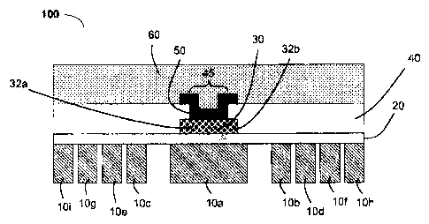
[0029] FIG. 1 shows an exemplary EAS tag 100, including capacitor
plate 10a, inductor
coil 10b-10h, dielectric film 20, semiconductor component 30, interlayer
dielectric 40, capacitor
plate 50, conductor 55 and passivation 60. A key feature of the present EAS
tag 100 is
semiconductor component 30, which enables tag 100 to be operated in frequency
division and/or
frequency multiplication modes. In certain embodiments, semiconductor
component 30 further
enables use of EAS tag 100 at advantageous radio frequencies, such as 100-400
KHz, 13.56 MHz
or 900-950 MHz, as will be explained in greater detail below.
[0030] Generally, capacitor plate 10a and inductor 10b-10h comprise
an electrically
conductive material, preferably a first metal. As will be explained in greater
detail with regard to
the present method of manufacturing below, capacitor plate 10a and inductor
10b-10h (and, in
most cases, interconnect pad 10j [see, e.g., FIGS. 9A-9B] and the inductor
portion 10i electrically
connecting inductor coil portion 10h to interconnect pad 10j; see, e.g., FIG.
9B) may be
advantageously formed from a single sheet or foil of a metal or alloy.
However, in alternative
embodiments, the metal/alloy for capacitor plate 10a and inductor 10b-10i
(and, optionally,
interconnect pad 10j) may be conventionally deposited or printed onto the
backside of dielectric
film 20. The metal may comprise aluminum, titanium, copper, silver, chromium,
molybdenum,
tungsten, nickel, gold, palladium, platinum, zinc, iron, or a conventional
alloy thereof. Other
conductive materials may include conductive polymers such as doped
polythiophenes,
polyimides, polyacetylenes, polycyclobutadienes and polycyclooctatetraenes;
conductive
inorganic compound films such as titanium nitride, tantalum nitride, indium
tin oxideõ etc.; and
doped semiconductors such as doped silicon, doped germanium, doped silicon-
germanium,
doped gallium arsenide, doped (including auto-doped) zinc oxide, zinc sulfide,
etc. Also, the
metal/alloy for capacitor plate 10a and inductor 10b-lOg may comprise a multi-
layer structure,
such as aluminum, tantalum or zirconium deposited (e.g., by sputtering or CVD)
onto a thin
-8-
CA 02606964 2007-10-18
Docket No.: EDR0121CA
copper sheet or foil, or copper deposited (e.g., by electroplating) onto a
thin aluminum sheet or
foil. The metal for the capacitor plate 10a may be chosen at least in part
based on its ability to be
anodized into an effective dielectric. This includes Al, Ta and other metals.
In preferred
embodiments, the first metal comprises or consists essentially of aluminum.
[00311 In the present surveillance and/or identification device 100, the
inductor 10b-10i,
capacitor plate 10a and/or interconnect pad 10j [see, e.g., FIGS. 9A-9B] may
have a nominal
thickness of from 5 to 200 gm (preferably from 20 to 100 gm) and/or a
resistivity of 0.1-10
golun-cm (preferably from 0.5 to 5 gohm-cm, and in one embodiment, about 3
golun-cm).
While the capacitor plate 10a of FIG. 1 is located substantially in the center
of the device, it may
be located in any area of the device, in accordance with design choices and/or
preferences. Also,
capacitor plate 10a may have any desired shape, such as round, square,
rectangular, triangular,
etc., with nearly any dimensions that allow it to fit in and/or on the EAS tag
100. Preferably,
capacitor plate 10a has dimensions of (i) width, length and thickness, or (ii)
radius and thickness,
in which the thickness is substantially smaller than the other dimension(s).
For example,
capacitor plate 10a may have a radius of from 25 to 10,000 i.un (preferably 50
to 5,000 pm, 100
to 2,500 gm, or any range of values therein), or a width and/or length of 50
to 20,000 gm, 100 to
10,000 p.m, 250 to 5,000 gm, or any range of values therein.
100321 Inductor 10b-10i is shown in FIG. 9B to comprise a coil having
a first loop or ring
10b-10c, a second loop or ring 10d-10e, a third loop or ring 10f-10g, and a
fourth loop or ring
10h-10i, but any suitable number of loops or rings may be employed, depending
on application
requirements and design choices/preferences. Inductor 10b-10i may take any
form and/or shape
conventionally used for such inductors, but preferably it has a coil, or
concentric spiral loop,
form. For ease of manufacturing and/or device area efficiency, the coil loops
generally have a
square or rectangular shape, but they may also have a rectangular, octagonal,
circular, rounded or
oval shape, some other polygonal shape, or any combination thereof, and/or
they may have one
or more truncated corners, according to application and/or design choices
and/or preferences, as
long as each successive loop is substantially entirely positioned between the
preceding loop and
- 9 -
CA 02606964 2007-10-18
Docket No.: IDR0121CA
the outermost periphery of the tag/device. Referring back to FIG. 1, the
concentric loops or rings
of the inductor coil 10b-10h may have any suitable width and pitch (i.e.,
inter-ring spacing), and
the width and/or pitch may vary from loop to loop or ring to ring. However, in
certain
embodiments, the wire in each loop (or in each side of each loop or ring) may
independently
have a width of from 2 to 1000 pm (preferably from 5 to 500 pm, 10 to 200 pm,
or any range of
values therein) and length of 100 to 50,000 gm, 250 to 25,000 pm, 500 to
20,000 pm, or any
range of values therein (as long as the length of the inductor wire does not
exceed the dimensions
of the EAS device). Alternatively, the radius of each wire loop or ring in the
inductor may be
from 250 to 25,000 pm (preferably 500 to 20,000 pm). Similarly, the pitch
between wires in
adjacent concentric loops or rings of the inductor may be from 2 to 1000 gm, 3
to 500 pm, 5 to
250 pm, 10 to 200 pm, or any range of values therein. Furthermore, the width-
to-pitch ratio may
be from a lower limit of about 1:10, 1:5, 1:3, 1:2 or 1:1, up to an upper
limit of about 1:2, 1:1,
2:1,4:1 or 6:1, or any range of endpoints therein.
[0033] Similarly, interconnect pad 10j (which is generally configured
to provide electrical
communication and/or physical contact with conductor 55) may have any desired
shape, such a
round, square, rectangular, triangular, etc., with nearly any dimensions that
allow it to fit in
and/or on the EAS tag 100 and provide electrical communication and/or physical
contact with
conductor 55. Preferably, interconnect pad 10j has dimensions of (i) width,
length and thickness,
or (ii) radius and thickness, in which the thickness is substantially smaller
than the other
dimension(s). For example, interconnect pad 10j may have a radius of from 25
to 2000 pm
(preferably 50 to 1000 pm, 100 to 500 pm, or any range of values therein), or
a width and/or
length of 50 to 5000 gm, 100 to 2000 gm, 200 to 1000 pm, or any range of
values therein.
[0034] Use of a substrate formed from a thin metal sheet or foil
provides a number of
advantages in the present invention. For example, one of the electrodes of the
device (preferably,
a gate and/or capacitor plate 10a) can be formed from the metal sheet or foil.
A thin metal sheet
or foil (which may have a major surface composed primarily of Al or Ta)
provides a convenient
source for dielectric film 20 by a relatively simple and straight-forward
process technology, such
-10-
CA 02606964 2007-10-18
Docket No.: IDR0121CA
as anodization. A metal sheet or foil also provides a conductive element that
can be formed into
an inductor coil or antenna using conventional metal film process technology.
Also, metal sheets
and/or foils have suitable high-temperature processing properties for
subsequent processing steps
(such as those described below with regard to the present method of
manufacturing), unlike many
[0035] The dielectric film 20 preferably is designed and made such
that application of a
deactivating radio frequency electromagnetic field induces a voltage
differential in the MOS
capacitor across dielectric film 20 that will deactivate the tag/device (e.g.,
a voltage differential
of about 4 to about 50 V, preferably about 5 to less than 30 V, more
preferably about 10 to 20 V,
[0036] As mentioned above, the semiconductor component 30 generally
comprises a
semiconductor, preferably a Group WA element. Preferably, the Group WA element
comprises
silicon. Alternatively, the Group WA element may consist essentially of
silicon or silicon-
- 11 -
__________________________________ CA 02606964 2007-10-18
Docket No.: IDR0121CA
of an elemental or compound semiconductor, the semiconductor component 30 may
further
comprise an electrical dopant. In the case of silicon or silicon-germanium,
the dopant may be
selected from the group consisting of boron, phosphorous and arsenic,
typically in a conventional
concentration (e.g., light or heavy, and/or from 1013 to 10 - -15,
10" to 1017, 1016 to 1018, 1017 to
1019, 1019 to 1021 atoms/cm2 or any range of values therein). For example, it
may be
advantageous to dope the semiconductor component 30 in order to improve the
frequency
response. A simple RC analysis suggests that conductivities of 2 x 10⁻² S/cm
or higher may be
required for high Q 13.56 MHz operation. This represents a lower limit in such
an application.
It may also be advantageous to heavily dope the near or upper surface region
of the
semiconductor component, or provide a second heavily-doped semiconductor
component (e.g.,
having a dopant concentration within the last two ranges described above)
adjacent to the first
semiconductor component, to assist in low resistance contact formation and
reduce the parasitic
series resistance of the device.
100371 Although the semiconductor component 30 may take nearly
any form with nearly
any dimensions, preferably it has a layered form, in that it may have
dimensions of (i) width,
length and thickness, or (ii) radius and thickness, in either case the
thickness being substantially
smaller than the other dimension(s). For example, the semiconductor component
30 may have a
thickness of from 30 nm to 500 nm, preferably from 50 nm to 200 nm, but a
radius of from 5 to
10,000 pm, (preferably 10 to 5,000 pm, 25 to 2,500 pm, or any range of values
therein), or a
width and/or length of 10 to 20,000 pm, 25 to 10,000 pm, 50 to 5,000 pm, or
any range of values
therein. Semiconductor component 30 may also comprise a multilayer structure,
such as a metal
suicide layer on a silicon-containing layer, successive n+/n- doped silicon
films, or alternating n-
doped and p-doped silicon films (each of which may comprise multiple layers of
differing dopant
concentrations, or which may have an intrinsic semiconductor layer between
them) to form a
conventional p-n, p-i-n or Schottky diode (in which case the semiconductor
component 30 may
have a second conductor in electrical communication with a different layer of
semiconductor
component 30 than conductor 55), etc. In the case of a diode structure, the
MOS dielectric may
-12 -
__________________________________ CA 02606964 2007-10-18
Docket No.: IDR0121CA
be omitted or locally removed to facilitate electrical contact between the
device electrodes and
the internal semiconducting components. This could be facilitated with the use
of one or more
printed (or otherwise deposited) masking materials prior to the anodization,
or through a local
removal process after the dielectric formation. In the case where the
semiconductor is in direct
contact with the inductor/capacitor electrode metal, it may be advantageous to
provide a metallic,
intermetallic or other type of barrier layer to prevent detrimental
interdiffusion or "spiking"
through the device, such as is known to be the case for Al and Si at elevated
temperatures.
100381 Conductor 55 generally provides electrical communication
between the
semiconductor component 30 and the inductor 10b-10h, but in most of the
present EAS and/or
RFID tags, conductor 55 generally further comprises a second capacitor plate
50 (i) capacitively
coupled (or complementary) to the first capacitor plate 10a and (ii) in
substantial physical contact
(e.g., having a major surface in contact) with the semiconductor component 30.
While conductor
55 and capacitor plate 50 are preferably formed at the same time from the same
material(s), they
may be formed separately and/or from different materials. Also, while
conductor 55 may
comprise any electrically conductive material, generally conductor 55
comprises a second metal,
which may be selected from the same materials and/or metals described above
for the first
capacitor plate 10a and/or inductor 10b-10h. In preferred embodiments, the
second metal
comprises or consists essentially of silver, gold, copper or aluminum (or a
conductive alloy
thereof).
100391 Conductor 55 (and, by association, capacitor plate 50 and
interconnect pad 58)
may take nearly any form with nearly any dimensions, but preferably, it has a
layered form, in
that it may have dimensions of width, length and thickness, in which the
thickness is smaller than
the other dimension(s). For example, conductor 55 (and thus, second capacitor
plate 50 and
interconnect pad 58) may have a thickness of from 30 urn to 5000 nm,
preferably from 50 nm to
2000 nm, more preferably from 80 nm to 500 nm. Second capacitor plate 50 may
have radius,
width and/or length dimensions that substantially match (or that are slightly
greater than or
slightly less than) those of first capacitor plate 10a (e.g., a radius of from
20 or 30 to 10,000 gm,
-13-
CA 02606964 2007-10-18
Docket No.: EDR0121CA
40 or 60 to 5,000 gm, 80 or 125 to 2,500 pm, or any range of values therein;
or a width and/or
length 01 40 or 60 to 20,000 pm, 80 or 125 to 10,000 gm, 150 or 250 to 5,000
gm, or any range
of values therein).
100401 Furthermore, in addition to second capacitor plate 50,
conductor 55 may comprise
(i) a pad portion 58 for electrical communication with inductor 10b-10h and
(ii) one or more wire
portions electrically connecting capacitor plate 50 and pad portion 58. As for
other conductive
structures in the present device, the wire portion(s) may have a width of from
2 to 1000 pm
(preferably from 5 to 500 gm, 10 to 200 gm, or any range of values therein)
and length of 100 to
25,000 pm, 250 to 20,000 gm, 500 to about 15,000 pm, or any range of values
therein (as long as
the length of the inductor wire does not exceed the dimensions of the LAS
device 100, or half of
such dimensions if capacitor plate 50 is in the center of device 100, as the
case may be). Pad
portion 58 generally has the same thickness as conductor 55, and may have any
suitable shape
(e.g., square, rectangular, round, etc.). In various embodiments, pad portion
58 has a width
and/or length of from 50 to 2000 pm, 100 to about 1500 pm, 200 to 1250 gm, or
any range of
values therein; or a radius of from 25 to 1000 gm, 50 to 750 pm, 100 to 500
gm, or any range of
values therein. In general, it may be advantageous to minimize the parasitic
capacitance resulting
from overlap of the capacitor pad not directly over the semiconductor
component and wire
connection by minimizing length and width of these features.
100411 In the present EAS device, the combination of the
semiconductor component 30
and the second capacitor plate 50 effectively forms a nonlinear capacitor with
the corresponding
portion of the dielectric film 20 and the complementary first capacitor plate
10a. Below a
predetermined threshold voltage (or a predetermined voltage differential
across dielectric film 20
and semiconductor component 30), second capacitor plate 55 functions as the
capacitor plate
complementary to first capacitor plate 10a, and dielectric film 20 and
semiconductor component
30 together function as the capacitor dielectric between first and second
capacitor plates 10 and
55. However, above the predetermined threshold voltage (or predetermined
voltage differential),
charge carriers (e.g., electrons) may be collected and/or stored in
semiconductor component 30,
- 14-
CA 02606964 2007-10-18
Docket No.: IDR0121CA
generally near the interface of the semiconductor component 30 and dielectric
film 20, thereby
changing the capacitive properties of the circuit. Thus, the capacitance
and/or other capacitive
properties of the circuit typically vary in dependence on the voltage across
the capacitor,
effectively making a nonlinear capacitor from the combination of second
capacitor plate 55,
semiconductor component 30, dielectric film 20 and first capacitor plate 10a.
In various
embodiments, the predetermined threshold voltage is from -10y to 10V, from
about -5V to about
5V, from about -1V to about 1V, or any range of voltages therein.
Alternatively, the highest
slope of the C-V curve of such a capacitor may occur at a voltage of from -5V
to 5V, -1V to 1V,
any range of voltages therein, or ideally, about OV.
Electrical dopant concentrations in the
semiconductor component may also be used to control the shape and slope(s) of
the CV curve.
The transition with changing bias across the device from the high capacitance
state of the MOS
capacitor device when charge is being stored at the oxide-semiconductor
interface (such as in the
accumulation mode of MOS device operation), to the mode where incremental
charge is being
stored at location(s) extending through the semiconductor (the so-called
depletion mode), and
therefore with a decreasing capacitance, can be a direct function of the
dopant profile.
[0042]
The present EAS device may further comprise an interlayer dielectric 40
between
the dielectric film 20 and the conductor 55. The interlayer dielectric 40
generally includes a via
45 at a location overlapping with at least part of the semiconductor component
30. FIG. 1 shows
a first embodiment in which the semiconductor component 30 has a peripheral
region (or
periphery) 32a-32b, and the interlayer dielectric 40 is also between the
periphery 32a-32b and the
conductor 50. In an alternative embodiment (see, e.g., FIG. 11A), the
semiconductor component
is entirely within the via 45. Referring back to FIG. 1, via 45 preferably has
a radius, or
alternatively, width and/or length dimensions, substantially the same as
second capacitor plate
50. However, in the embodiment of FIG. 1, semiconductor component 30 may have
radius,
25 width and/or length dimensions greater than those of via 45.
[0043]
The interlayer dielectric 40 may comprise any electrically insulative material
providing the desired dielectric properties, as for dielectric film 20.
However, thickness
- 15-
CA 02606964 2007-10-18
Docket No.: IDR0121CA
tolerances of interlayer dielectric 40 are not as small in absolute terms as
those of dielectric film
20, so polymers such as polysiloxanes, parylene, fluorinated organic polymers,
etc., may be more
easily used in interlayer dielectric 40. However, in preferred embodiments,
interlayer dielectric
40 comprises an oxide and/or nitride of a second Group WA element, which may
further contain
conventional boron and/or phosphorous oxide modifiers in conventional amounts.
Thus, the
second Group NA element may comprise or consists essentially of silicon, in
which case the
interlayer dielectric 40 may comprise or consist essentially of silicon
dioxide, silicon nitride,
silicon oxynitride, a borosilicate glass, a phosphosilicate glass, or a
borophosphosilicate glass
(preferably silicon dioxide). To minimize parasitic capacitances with inductor
10b-10i, interlayer
dielectric 40 may have a thickness of at least 1 pm, and preferably from 2 to
25 gm, 5 to 10 gm,
or any range of values therein.
[0044] The embodiment shown in FIG. 1 A has certain advantages over
the alternative
embodiment that would result from the structure of FIGS. 11A-B. For example,
in the case of a
printed semiconductor component, potentially detrimental edge morphology, such
as edge spikes
and/or relatively appreciable thickness variations near the feature edge, may
be present. By
positioning the active area of the MOS nonlinear capacitor away from these
potentially
detrimental edge regions (e.g., when the ILD via hole 45 is smaller than the
printed
semiconductor feature dimensions), the impact of edge morphology can be
reduced. However, as
will be discussed below with regard to FIGS. 11A-B, the alternative embodiment
produced from
the structure of FIGS. 11A-B also has certain advantages as well. For example,
nonlinear
capacitor variations may be minimized in the alternative embodiment of FIGS.
11A-B, thereby
improving suitability for applications requiring minimal deviations from an
ideal and/or
predetermined resonance frequency.
[0045] The present device may further comprise a passivation layer 60
over the conductor
55 and interlayer dielectric 40. Passivation layer 60 is conventional, and may
comprise an
organic polymer (such as polyethylene, polypropylene, a polyimide, copolymers
thereof, etc.) or
an inorganic dielectric (such as aluminum oxide, silicon dioxide [which may be
conventionally
-16-
CA 02606964 2011-11-10
Docket No.: IDR012 CA
doped and/or which may comprise a spin-on-glass], silicon nitride, silicon
oxynitride, or a
combination thereof as a mixture or a multilayer structure). Passivation layer
60 generally has
the same width and length dimensions as the EAS device, and it may also have
any thickness
suitable for EAS, RF and/or RF1D tags or devices. In various embodiments,
passivation layer 60
has a thickness of from 3 to 100 gm, from 5 to 50 inn, 10 to 25 gm, or any
range of values
therein.
[0046] The present device may also further comprise a support and/or
backing layer (not
shown) on a surface of the inductor 10b-10h opposite the dielectric film 20.
The support and/or
backing layer are conventional, and are well known in the EAS and RFID arts
(see, e.g., U.S. Pat
Appl. Publication No. 2002/0163434 and U.S. Pat. Nos. 5,841,350, 5,608,379 and
4,063,229
). Generally, such support
and/or backing layers provide (1) an adhesive surface for subsequent
attachment or placement
onto an article to be tracked or monitored, and/or (2) some mechanical support
for the EAS
device itself. For example, the present EAS tag may be affixed to the back of
a price or article
identification label, and an adhesive coated or placed on the opposite surface
of the EAS tag
(optionally covered by a conventional release sheet until the tag is ready for
use), to form a price
or article identification label suitable for use in a conventional EAS system.
Exemplary Methods for Making a MOS EAS and/or RE Tag/Device
[0047] In one aspect, the present invention concerns a method for
making a surveillance
and/or identification device, comprising the steps of: (a) depositing a
semiconductor material or
semiconductor material precursor on a dielectric film, the dielectric film
being on an electrically
functional substrate; (b) forming a semiconductor component from the
semiconductor material or
semiconductor material precursor; and (c) fowling a conductive structure at
least party on the
semiconductor component, the conductive structure being configured to provide
electrical
communication between the semiconductor component and the electrically
functional substrate;
and (4) etching the electrically functional substrate to form (I) an inductor
and/or (ii) a second
capacitor plate capacitively coupled to the semiconductor component under one
or more
predetermined conditions. In a preferred embodiment the depositing step
comprises printing a
- 17 -
CA 02606964 2011-11-10
Docket No.: D3R0121CA
liquid-phase Group IVA element precursor ink on the dielectric film. Printing
an ink, as opposed
to blanket deposition, photolithography and etching, saves on the number of
processing steps, the
length of time for the manufacturing process, and/or on the cost of materials
used to manufacture
the EAS device. Thus, the present method provides a cost-effective method for
manufacturing
nonlinear EAS devices.
[0048] A first exemplary method for manufacturing the present EAS tag
is described
below with reference to FIGS. 2A-9B. An alternative process for a subset of
the exemplary
method steps is described below with reference to FIGS. 10A-11B.
The Substrate
[0049] FIGS. 2A-2B respectively show cross-sectional and top-down views of
an
electrically functional substrate 10, which in various embodiments, comprises
a metal sheet or
metal foil (and in one embodiment, a thin aluminum sheet). Prior to subsequent
processing,
substrate 10 may be conventionally cleaned and smoothed. This surface
preparation may be
achieved by chemical polishing, electropolishing and/or oxide stripping to
reduce surface
roughness and remove low quality native oxides. A description of such
processes is given in,
"The Surface Treatment and Finishing of Aluminum and Its Alloys," by P. G.
Sheasby and R.
Pinner, sixth edition, ASM International, 2001
100501 As described above, the metal sheet/foil may have a nominal
thickness of 20-100
pm and/or a resistivity of 0.1-10 pohm-an. A metal sheet/foil is
advantageously used in the
present method because it may be (1) electrochemically anodized to
reproducibly and/or reliably
provide a suitable dielectric film, (2) later formed into the inductor and
lower capacitor plate,
and/or (3) serve as a mechanically and/or physically stable substrate for
device processing during
the first part of the manufacturing process.
-18-
CA 02606964 2011-11-10
Docket No.: IDR0121CA
Forming the Dielectric Film
[0051] Referring now to FIGS. 3A-3B (which respectively show cross-
sectional and top-
down views), the method further comprises the step of forming a dielectric
film 20 on the
electrically functional substrate 10. In preferred embodiments, the dielectric
film 20 has a
thickness of from 50 to soca and/or a breakdown voltage of from about 5V to
less than 50V,
preferably from 10V to 20V. In one implementation in which substrate 10
comprises or consists
essentially of a metal sheet or metal foil, the step of forming the dielectric
film comprises
anodizing the metal sheet or metal foil. A thin anodized dielectric metal
oxide film having a
controlled breakdown in a voltage range preferably from about 10 to about 20 V
provides a
reliable deactivation mechanism for the EAS tag.
[00521 Anodization to form a MOS dielectric and/or deactivation
dielectric is a known
process. A typical thickness for the dielectric film 20 is from 100 to 200A,
which may
correspond to a breakdown voltage in the above range, particularly when the
dielectric film 20
consists essentially of aluminum oxide. In such electrochemical anodization, a
rule of thumb is
that one may obtain a thickness of 1.3nmN + 2nm (see J. App!. Phys., Vol. 87,
No. 11, 1 June
2000, p. 7903 ).
[00531 Barrier-type anodic oxide films are usually formed in dilute
solutions of organic
acids, like tartaric acid or citric acid, or in dilute solution of inorganic
salts or acids (for example,
ammonium pentaborate or boric acid). Ethylene glycol may be mixed with water
in those
solutions, or even completely replace the water, as is often the case of a
pentaborate salt. The pH
of the electrolyte is usually adjusted to be between 5 and 7. The electrolytic
bath is usually, but
not exclusively, kept at room temperature. The Al foil or substrate is
connected to the positive
pole of a power supply (the anode) while the counter-electrode (usually a
metal grid) is
- 19 -
CA 02606964 2007-10-18
Docket No.: IDR0121CA
connected to the negative pole of the power supply (the cathode). Anodized
films may be formed
in a continuous and/or multi-step process. In an exemplary two step-process,
during a first
period of time, the voltage is increased at a constant current up to a voltage
corresponding to
about the desired thickness according to the formula: Vfiõ,d = [desired
thickness in nm]/1.2-1.4,
where Vfinai is the final voltage at the end of the first period of time. The
constant current during
this first phase may be from 10 microamps/cm2 to 1 amp/cm2, preferably from
100
microamps/cm2 to 0.1 amp/cm2. The rate of voltage increase may be from 0.1 to
100 V/min,
preferably from about 10 to 50 V/min. In one implementation, the voltage
increase rate is about
30 V/min. Vfinal typically has a value at least that of the desired maximum
breakdown voltage of
the anodized film, and usually, about 1 to 2 times that desired maximum
breakdown voltage.
Then, during a second period of time, anodization current decreases while a
constant voltage
(equal to the final voltage from the first period of time) is maintained,
during which period the
dielectric properties are improved. The second period of time may be from 10
seconds to 60
minutes and in one implementation, about 15 min.
[0054] The dielectric breakdown voltage may be directly related to the
voltage applied
during the electrochemical anodization process to form the dielectric (Vni.d).
For example, as
discussed above, the breakdown voltage generally cannot exceed Vi. Typically,
however, the
breakdown voltage is from 50 to about 90% of Vfintd, more typically about 60
to about 80% of
V. There may also be a relationship between the breakdown voltage and the
current applied
in the first phase of anodization, in that the higher the current, generally
the closer the breakdown
voltage comes to Vfinal.
Forming the Semiconductor Component
[0055] Referring now to FIGS. 4A-4B (which respectively show cross-
sectional and top-
down views of the EAS device 100), the method further comprises the step of
depositing a
semiconductor component 30 on the dielectric film 20. As described above, the
component 30
may comprise any material that provides a nonlinear response to an RF field.
In general, any
- 20 -
CA 02606964 2011-11-10
Docket No.: TDR0121CA
method for depositing the semiconductor component material may be used, such
as printing, or
conventional blanket deposition (e.g., by chemical vapor deposition [CVD], low
pressure CVD,
sputtering, electroplating, spin coating, spray coating, etc.),
photolithography and etching.
Certain photopatternable functional materials that may have nonlinear
properties, and methods
for their deposition and use, are disclosed in copending U.S. Application No.
10/749,876, filed
December 31, 2003
. Typical semiconductor component film thicknesses may be
from 50 to 200 nm. The film thickness may be chosen to optimize (i) the
maximum swing of the
capacitance and/or (ii) the slope of the C(V) curve (see, e.g., FIG. 13 and
the discussion thereof
below) and the series resistance-limited frequency response of the EAS tag.
(0056)
In preferred embodiments, semiconductor component 30 comprises a
semiconductor material, such as one or more Group WA elements (e.g., silicon
and/or
germanium), a so-called 111-V" material (e.g., GaAs), an organic or polymeric
semiconductor,
etc. Thus, in one implementation, depositing the semiconductor material or
semiconductor
material precursor comprises depositing a liquid-phase Group WA element
precursor ink on the
dielectric film. Suitable liquid-phase Group WA element precursor inks and
methods for
printing such inks are disclosed in copending U.S. Application Nos. 10/616,147
and 10/789,317,
respectively filed July 8, 2003 and February 27, 2004
. Use of a precursor ink is advantageous in that the depositing step may
thereby
comprise printing the liquid-phase Group WA element precursor ink on the
dielectric film, as
discussed above. Printing may comprise inkjet printing, microspotting,
stenciling, stamping,
syringe dispensing, pump dispensing, screen printing, gravure printing, offset
printing,
flexography, laser forward transfer, or local laser CVD.
[0057) When using a Group WA element precursor ink, the step of forming the
semiconductor component generally comprises curing the Group WA element
precursor, and
may further comprise drying the liquid-phase Group WA element precursor ink
before curing the
Group WA element precursor. See copending U.S. Application Nos. 10/616,147,
10/789,317
- 21 -
CA 02606964 2011-11-10
Docker No.: JDR0121CA
and 10/789,274, respectively filed July 8, 2003, February 27, 2004 and
February 27, 2004
. Typically, although not necessarily always,
the liquid-phase Group WA element precursor ink further comprises a solvent,
invferably a
cycloalkane. In preferred implementations, the Group WA element precursor
comprises a
compound of the formula Anlii,+y, where n is from 3 to 12, each A is
independently Si or Ge, and
y is an even integer of from n to 2n+2, more preferably a compound of the
formula (AIL), where
n is from 5 to 10, each A is independently Si or Ge, and each of the n
instances of z is
independently 1 or 2. Use of local printing of a liquid semiconductor
precursor, preferably a
silane-based precursor to Si or doped Si (see, e.g., U.S. application serial
nos. 10/616,147 and
10/789,317), directly onto dielectric film 20 to form part of an RF active MOS
structure is cost
effective due to efficient semiconductor precursor materials usage and the
combination of
deposition and patterning into one inexpensive printing step.
ROW The semiconductor deposition process may also require UV or
thermal curing
processes to fix the layer and/or convert the precursor to an active
semiconducting layer and/or
remove unwanted precursor components or byproducts such as carbon (elemental
carbon or a
carbon-containing compound) or excess hydrogen (particularly if laser
recrystallization is to be
used immediately after semiconductor film formation). In such embodiments, the
semiconductor
or semiconductor precursor may be also deposited by spin coating with
simultaneous irradiation,
as disclosed in copending U.S. Application No. 10/789,274, filed on February
27, 2004
,or by
other techniques, including bath deposition. Furthermore, the semiconductor
may be deposited
by other processes including large area (e.g., blanket) or local sputtering,
CVD, laser forward
transfer, or other processes.
100591 It is generally desirable to increase the frequency response of the
MOS capacitor
circuit on the EAS device and provide a low series resistance for the
circuitry in the EAS device
-22 -
CA 02606964 2007-10-18
Docket No.: IDR0121CA
to enable high frequency operation (e.g., in the range of 125 KHz and above).
To achieve
sufficiently low series resistance and/or increased frequency response, one
may recrystallize the
semiconductor material used for the semiconductor component 30. Such
recrystallization can
improve the carrier mobility and/or dopant activation of the semiconductor.
Mobilities
approaching 10 cm2/vs and higher may be required for low dissipation and/or
effective high Q.
Low dissipation generally requires low series resistance, preferably less than
5 Ohms for the
entire circuit, along with a large parallel resistance (generally provided by
a low leakage
dielectric) of at least 104 Ohms, preferably? 105 Ohms, most preferably >106
Ohms. Effective
high Q provides low field and/or high read range operation in MHz range
frequencies and higher.
Reaystallization may comprise irradiating with a laser sufficiently to
recrystallize the
semiconductor, heating at a temperature and time below the damage threshold of
the metal
sheet/film 10 but sufficient to recrystallize the semiconductor, and/or
inducing or promoting
semiconductor crystallization using a metal (e.g., Ni, Au, etc.) at a
temperature generally lower
than the semiconductor recrystallization temperature (e.g., 400 C or less,
300 C or less, or 250
C or less).
10060] Heavily doping, or alternatively, siliciding the semiconductor
material may also
increase the frequency response of the EAS tag MOS capacitor circuit, and form
a low
resistance/barrier contact between the semiconductor component 30 and an
electrode (e.g., upper
capacitor plate 50 and conductor 55, shown in FIGS. 7A-7B). A doped
semiconductor layer 30
may be formed by conventionally implanting a conventional semiconductor
dopant, diffusing
such a dopant into the semiconductor material from a solid or vapor dopant
source, by printing a
doped semiconductor or semiconductor precursor such as a B- or P-containing
(cyclo)silane (see
copending U.S. Application Nos. 10/616,147 and 10/789,317, respectively filed
July 8, 2003 and
February 27, 2004 [Attorney Docket Nos. KOV-004 and IDR0020, respectively],
the relevant
portions of each of which are incorporated herein by reference), and/or by
laser forward transfer
of a doped semiconductor layer or dopant diffusion source layer. Referring now
to FIGS. 5A-5B
(which respectively show cross-sectional and top-down views of EAS device
100), a metal
- 23 -
CA 02606964 2007-10-18
Docket No.: MR0121CA
suicide layer 35 may be formed on semiconductor component 30 by, e.g., blanket
depositing a
metal film, annealing to form the metal suicide, and removing the non-
silicided metal by
selective etching. Suitable metal suicides include titanium suicide, tungsten
suicide, cobalt
suicide, molybdenum suicide, and others.
[0061] Heavily doped or silicided contacts between upper capacitor plate 50
and
semiconductor layer 30 may also allow for improved ohmic contact and/or
reduced contact
resistance. The carrier concentration of the doped contact layer is preferably
> 10Ig cm4. This
reduces the overall series resistance of the EAS device and results in higher
Q and large relative
capacitance changes for the MOS capacitor in the EAS device, as more voltage
may be present
across the active semiconductor region of the device. Thus, and now referring
to FIGS. 5A-5B,
the present manufacturing method may further comprise printing a contact layer
35 onto the
active silicon semiconductor layer 30 using, e.g., a silicon-containing ink
further containing one
or more dopants. This process step has the advantage of not requiring a high
temperature
diffusion and/or activation step. The dopant may be active upon curing the
silicon precursor ink,
or it may be activated by conventional thermal, optical, or laser annealing,
including activation
during a combined dopant activation and =crystallization step.
100621 It may also be desirable to provide a relatively low level of
doping (a
concentration of < 5 x 10" cm-3 electrically active dopant atoms) in the bulk
of the active
semiconductor layer 30 to control the CV slope of the device and also reduce
the series resistance
of the semiconductor component, thereby allowing higher Q and/or higher
frequency operation.
Simple RC calculations of the EAS device performance indicate that
conductivities of the
semiconductor component film 30 may need to be higher than ¨2.5x10⁻² L1-1 cm-1
for device
operation at a frequency of about 13.56 MHz. This may be achieved with (1)
mobilities near 10
cm2/vs and above and (2) electrically active doping levels of ¨1017 cm4.
(These calculations do
not account for contact resistance and/or contact barriers, and actual
conductivity requirements
may be higher. For example, assuming a 0.5 LI contact resistance, the
conductivity requirements
-24 -
CA 02606964 2007-10-18
Docket No.: IDR0121CA
would increase to approximately 4.5x10⁻²
cm', and the doping level would increase
correspondingly.)
[00631
In addition, the semiconductor component may comprise a multilayer structure
30/35. For example, and continuing to refer to FIGS. 5A-5B, successive silane
coating/curing
processes may be used to form an n- doped silicon film 30 and an n+ doped
silicon film 35
thereon, an n-doped silicon film 30 and a p-doped silicon film 35 thereon or
vice versa (each of
which may comprise multiple layers of differing dopant concentrations, or
which may have an
intrinsic semiconductor layer between them) to form a conventional p-n, p-i-n
or Schottky diode
(in which case silicon film 35 may only partially overlie silicon film 30, and
silicon film 30 may
be in electrical communication with a second conductor and/or a second
interconnect pad in
electrical communication with conductor 55 or logic circuitry [not shown]), or
more complex
alternating n-doped and p-doped silicon films, etc.
Forming the Interlayer Dielectric
[00641
Referring now to FIGS. 6A-6B (which respectively show cross-sectional and top-
down views of EAS device 100), the present method of manufacturing a
surveillance and/or
identification device may further comprise the step of depositing an
interlayer dielectric (ILL)) 40
on at least a part of the dielectric film 20. The ILD provides an electrical
separation, in terms of
leakage and capacitance, between the inductor 10b-10i and the top electrode
strap 55 (see, e.g.,
FIG. 1), which may be highly desired and/or necessary for EAS tag operation.
[0065] In one embodiment, the step of depositing the interlayer dielectric
40 is performed
after the step of forming the semiconductor component 30, and in an
alternative embodiment (see
FIGS. 10A-11B and the corresponding discussion thereof below), the step of
depositing the
interlayer dielectric 40 is performed before the step of forming the
semiconductor component 30.
In either case, the interlayer dielectric 40 may be blanket deposited over the
entire device and
selected portions thereof removed (e.g., by conventional photolithography and
etching), or
- 25 -
CA 02606964 2007-10-18
Docket No.: IDR0121CA
alternatively, interlayer dielectric 40 may be selectively deposited on one or
more predetermined
portions of dielectric film 20 (and, optionally, on one or more predetermined
portions of
semiconductor component 30 or upper semiconductor component layer 35) by,
e.g., printing an
interlayer dielectric precursor thereon. Also, in either case, the interlayer
dielectric may have a
[0066] In the case where the step of depositing the interlayer
dielectric 40 is performed
after the step of forming the semiconductor component 30, the interlayer
dielectric 40 is also
deposited on at least a part of the semiconductor component 30. In the case
where the interlayer
dielectric 40 is blanket deposited, the method generally further comprises the
step of forming a
[0067] Thus, in some implementations, the step of depositing the
interlayer dielectric 40
may comprise the steps of (i) printing a liquid-phase interlayer dielectric
precursor ink on at least
- 26-
CA 02606964 2011-11-10
Docket No.: B3R0121CA
to 10, each A is independently Si or Ge, and each of the n instances of z is
independently 1 or 2.
In the case of the ILD 40, the corresponding silicon and/or germanium oxide
film is formed by
curing the Group WA element precursor film in an oxidizing atmosphere (e.g.,
at a temperature
of 300 C, 350 C or 400 C or more, but less than the melting temperature of
the substrate 10, in
the presence of oxygen, ozone, N20, NO2, or other oxidizing gas, which may be
diluted in an
inert carrier gas such as nitrogen, argon or helium). Of course, the silane-
based Si or Si02
precursor film (see, e.g., U.S. application serial nos. 10/789,317 and
10/789,274
, each filed on February 27, 2004
) may also be blanket deposited and photolithographically etched.
100681 Other solution-based dielectrics, including spin on glasses, organic
dielectrics,
etc., may be applied by printing or other conventional coating steps. Suitable
ILD materials
include spin on glasses (which may be photodefinable or non-photodefinable, in
the latter case
patterned by direct printing or post deposition lithography); polyimides
(which may be
photodefmable and/or thermally sensitized for thermal laser patterning, or non-
photodefinable for
patterning by direct printing or post deposition lithography); BCB or other
organic dielectrics
such as SiLK. dielectric material (SILK is a registered trademark of Dow
Chemical Co.,
Midland, MI); low-k interlayer dielectrics formed by sol-gel techniques;
plasma enhanced (PE)
TEOS (i.e., Si02 formed by plasma-enhanced CVD of tetraethylorthosilicate);
and laminated
polymer films such as polyethylene (PE), polyester, or higher temperature
polymers such as PES,
polyimide or others that are compatible with subsequent high temperature
processing.
100691 An additional "via" or opening in ILD 40 is generally required
to allow contact
between the "pad" end 10j of the inductor coil 10b-10i and the interconnect
pad 58 of the top
electrode 55 (see, e.g., FIGS. 9A-9B). The ILD 40 may be printed in a pattern
providing for such
contact, or the additional opening may be formed in a later etch step, which
may be performed by
laser ablation, mechanical penetration or other etching or dielectric removal
technique. Thus,
after ILD 40 is printed, defined and/or patterned, dielectric film 20 is
similarly patterned
(t)pically by conventional wet or dry etching), using ILD 40 (and
semiconductor component
- 27 -
CA 02606964 2007-10-18
Docket No.: IDR0121CA
30/35) as a mask, resulting in the structure shown in FIGS. 6A-6B. For
convenience in showing
the interconnect structure at the lower left-hand corner of tag 100, FIG. 6A
is a cross-sectional
view of the tag 100 of FIG. 6B with the left-hand side showing the cross-
section along the
diagonal axis from the center of tag 100 to point A, and the right-hand side
showing the cross-
section along the axis from the center of tag 100 to point A'.
[0070] The process flow of FIGS. 3A-6B, with formation of ILD 40
following the
deposition of semiconductor component 30, has some advantages, including the
fact that silicon
processing in semiconductor component formation, which may include high
temperatures, UV
irradiation and/or laser exposure, does not necessarily and/or directly affect
the ILD 40, as the
ILD 40 can be added after semiconductor component formation. The critical
planar dimensions
may be controlled by the conductor deposition process, the extent of a heavily
doped contact
layer that can define the effective area of the MOS capacitor, or by local
recrystallization (where
the lateral extent of the laser exposed regions controls the effective area,
and therefore, the
nominal capacitance of the device by limiting the active recrystallized and/or
dopant activated
region of the device). Also, as mentioned above, by using a via 45 smaller
than the printed
semiconductor component dimensions and thus positioning the active area of the
MOS capacitor
away from potentially detrimental edge regions, the impact of potentially
detrimental edge effects
can be reduced. It may also be possible to use a high precision printing
technique, such as ink jet
printing, syringe dispensing, stenciling, screen printing, aerosol jet
printing, etc., to define the
capacitor size by printing a top capacitor plate where the overall capacitance
is partially or fully
defined by the line width and/or resolution of the printed conductor feature
(in this case,
capacitor plate 50).
[0071] Blanket deposition of the ILD 40 may be done by extrusion,
blade, dip, linear,
spin or other coating technique, as well as by local deposition techniques
such as printing or
dispensing. In the case of printing or dispensing, this may also serve the
purpose of patterning
the ILD 40. Patterning of the ILD layer 40 may be done by direct printing of
the 1LD precursor
materials (e.g., by UP, screen, gravure, flexography, laser forward transfer,
etc.) or indirect
- 28 -
CA 02606964 2007-10-18
Docket No.: IDR0121CA
patterning (such as with a photo- and/or thermo-patternable precursor material
that is exposed by
a photomask, thermal or laser pattern and developed, or extrinsically via a
patterning process
such as conventional photolithography, embossing or similar technique).
[00721 Referring now to FIGS. 10A-10B, in another version of the
manufacturing
process, formation of the ILD 40 and via 45 may precede the deposition of the
semiconductor
component 30 and/or its associated contact/doping/silicide layer(s) 35. This
alternative process
has the advantage that the surface energy and/or physical pattern of the ILD
40 may direct or
pattern the features of a printed semiconductor component 30, thereby
controlling the physical
dimensions of the nonlinear device.
100731 In this case, the physical steps and/or wetting properties of the
ILD 40 versus the
exposed area of the dielectric film 20 within via 45 may serve to pattern or
otherwise control the
extent to which the semiconductor component precursor solution is deposited or
printed, thereby
helping to control the tolerances of the circuitry on the EAS device 100. This
can be particularly
advantageous in non-swept EAS read systems, where the reader
interrogation/power signal is
fixed. In this case, the transponder's resonance must closely match that of
the reader signal in
order for good coupling to occur between the transponder and reader.
Controlling the effective
capacitor size through the patterning of the ILD 40 provides a means or
mechanism for limiting
the spread of the resonances of the tags (i.e., the tag-to-tag or lot-to-lot
resonance frequency
variation) due to manufacturing variations.
[0074] In this alternative process, the ILD 40 can define the effective
size of the
semiconductor component 30 (and, optionally, upper semiconductor component
layer 35) and/or
capacitor 55, and therefore control the tolerances for the capacitor size.
This may have
advantages where the processes for making or forming the nonlinear capacitor
elements may be
of relatively low placement or alignment accuracy (high speed printing, for
instance). The ILD
40 is of sufficient thickness that the overlap capacitance formed between the
top conductors
50/55 (including the capacitor plates and the strap) and the bottom conductors
(including the
- 29-
- ________________________________ CA 02606964 2007-10-18
Docket No.: IDR0121CA
bottom electrode plate 10a, inductor 10b-10i, and interconnect pad 10j) is not
significant in
comparison with the capacitance of the region contained within the LLD via 45.
100751 However, in the version of the manufacturing process
shown in FIGS. 4A-6B, the
ILD 40 and ILD via 45 are formed after depositing the semiconductor component
30/35. Again,
in this case, the extent of the high capacitance MOS active region is
effectively defined by the
size of via 45, and not the area of the printed semiconductor component 30/35.
It may be
advantageous for the via size to be significantly smaller than the
semiconductor component size
to reduce the impact of edge nonuniformities that may be present (e.g., edge
drying effects,
roughness, or chemical inhomogeneity that may occur at the edge of printed,
solution-deposited,
or etched semiconductor features).
Forming the Conductor
[0076] Referring now to FIGS. 7A-7B, the present method of
manufacturing a
surveillance and/or identification device generally comprises forming a
conductive structure 50,
generally configured to provide electrical communication between the
semiconductor component
30/35 and substrate 10 (from which, as will be seen in FIGS. 9A-9B and
discussed below, the
EAS circuit inductor and bottom capacitor plate can be subsequently formed).
In one
implementation, the step of forming the conductor 50 comprises printing a
conductor ink onto
the semiconductor component 30/35 and at least part of the inter-layer
dielectric 40 (and
optionally, onto at least part of the substrate 10). As for the semiconductor
component-forming
step(s), the step of forming the conductor may further comprises the step(s)
of drying and/or
curing the conductor ink. Alternatively, the step of forming the conductor
comprises depositing
the conductor onto semiconductor component 30/35, the interlayer dielectric,
and exposed
portion(s) of the substrate 10, and etching the conductor to form conductive
structure 55 and
upper capacitor plate 50. Thus, the method generally comprises the step(s) of
(1) forming the
conductive structure 50/55 such that it is in electrical communication with at
least one of (and
-30 -
CA 02606964 2007-10-18
Docket No.: IDR0121CA
preferably both of) the semiconductor component 30/35 and the substrate 10,
and/or (2) forming
the conductive structure 50/55 after the semiconductor component 30.
[0077] In preferred implementations, the top electrode (e.g.,
conductor 55) further
includes an interconnect pad 58 from the outside of the to-be-formed inductor
coil 10b-10h (see,
e.g., FIG. 1) and an upper, charge-injecting plate or electrode 50 of the MOS
capacitor. Similar
to the semiconductor element 30, the top electrode may be formed by printing
(e.g., by inkjet
printing, screen printing, syringe dispensing, micro-spotting, gravure
printing, offset printing,
flexographic printing or other printing method) one or more conducting inks or
conducting ink
precursors onto the upper surface of the structure of FIGS. 6A-6B in the
pattern shown in FIG.
7B.
[0078] Inclusion of dopants, siliciding components, or other agents
(work function
modulation agents and/or tunneling barrier materials) into conductive
structure 50 may reduce
the series resistance and increase the Q and overall tag performance. Such
series resistance
reduction may comprise (i) one or more additives in the top electrode ink
and/or (ii) depositing
one or more interlayer material(s) between the top electrode and the
underlying semiconductor
component 30/35.
Passivation
[0079] As shown in FIG. 8, after forming conductive structure 50, the
present
manufacturing method may further comprise the step of passivating (e.g.,
forming a passivation
layer 60) over the interlayer dielectric 40 and the conductive structure 50
(and, when exposed,
substrate 10). A passivation layer 60 generally adds mechanical support to the
EAS device,
particularly during the substrate etching process, and may prevent the ingress
of water, oxygen,
and/or other species that could cause the degradation or frequency drifting of
device
performance. The passivation layer 60 may be formed by conventionally coating
the upper
surface of the device 100 with one or more inorganic barrier layers such as a
polysiloxane and/or
- 31 -
CA 02606964 2007-10-18
Docket No.: IDR0121CA
a nitride, oxide and/or oxynitride of silicon and/or aluminum, and/or one or
more organic barrier
layers such as parylene, a fluorinated organic polymer (e.g., as described
above), or other barrier
material.
Forming the Inductor and/or Lower Capacitor Plate
[0080] FIGS. 9A-9B respectively show cross-sectional and bottom views of
EAS device
100, in which substrate 10 has been patterned and etched to form lower
capacitor plate 10a,
inductor 10b-10i and interconnect area 10j. Thus, the present manufacturing
method further
comprising the step of etching the electrically functional substrate,
preferably wherein the etching
forms an inductor and/or a capacitor plate (i) capacitively coupled to
semiconductor component
30 under one or more predetermined conditions (such as above the predetermined
threshold
voltage described above) and/or (ii) complementary to the upper capacitor
plate 50 formed as
part of the conductive structure 55.
[0081] The substrate 10 (see FIG. 8) can be patterned by conventional
photolithography,
or by contact printing or laser patterning of a resist material applied to the
backside (non-device
side) of substrate 10. The substrate 10 can then be etched with standard wet
(e.g., aqueous acid)
or dry (e.g., chlorine, boron trichloride) etches to form the capacitor plate
10a, inductor 10b-10i
and interconnect pad 10j. The patterning and/or etching steps may be
thermally, optically or
electrically assisted. The substrate 10 may also be patterned by direct means
such as milling,
laser cutting, stamping, or die-cutting.
[0082] A backing and/or support layer may be desired or required to provide
mechanical
stability and/or protection for the non-passivated side of the device 100
during later handling
and/or processing. Thus, the present manufacturing method may further comprise
the step of
adding a support or backing to the etched electrically functional substrate.
This backing layer
may be added by lamination to paper or a flexible polymeric material (e.g.,
polyethylene,
polypropylene, polyvinyl chloride, polytetrafluoroethylene, a polycarbonate,
an electrically
- 32 -
CA 02606964 2007-10-18
Docket No.: IDR0121CA
insulating polyimide, polystyrene, copolymers thereof, etc.) with the use of
heat and/or an
adhesive. Where the backing comprises an organic polymer, it is also possible
to apply the
backing layer from a liquid precursor by dip coating, extrusion coating or
other thick film coating
technology.
An Exemplary Method of Tracking Articles Using the Present EAS and/or RF
Tags/Devices
100831
The present invention further relates to method of detecting an item or object
in a
detection zone comprising the steps of: (a) causing or inducing a current in
the present device
sufficient for the device to radiate detectable electromagnetic radiation
(preferably at a frequency
that is an integer multiple or an integer divisor of an applied
electromagnetic field), (b) detecting
the detectable electromagnetic radiation, and optionally, (c) selectively
deactivating the device.
Generally, currents and voltages are induced in the present device sufficient
for the device to
radiate detectable electromagnetic radiation when the device is in a detection
zone comprising an
oscillating electromagnetic field. This oscillating electromagnetic field is
produced or generated
by conventional EAS and/or RFID equipment and/or systems. The present method
of use may
further comprise attaching, affixing or otherwise including the present device
on or in an object
or article to be detected. Furthermore, in accordance with an advantage of the
present device, it
may be deactivated by non-volatile shifting of the thresholds (i.e. position
of the CV curve
features versus voltage) or capacitance of the device in response to an
applied electromagnetic
field having sufficient strength and an effective oscillating frequency to
induce a current, voltage
and/or resonance in the device. Typically, the device is deactivated when the
presence of the
object or article in the detection zone is not to be detected or otherwise
known.
100841
The use of electronic article surveillance or security systems for detecting
and
preventing theft or unauthorized removal of articles or goods from retail
establishments and/or
other facilities, such as libraries, has become widespread. In general, EAS
systems employ a
label or security tag, also known as an EAS tag, which is affixed to,
associated with, or otherwise
- 33 -
CA 02606964 2007-10-18
Docket No.: IDR0121CA
secured to an article or item to be protected or its packaging. Security tags
may have many
different sizes, shapes and forms, depending on the particular type of
security system in use, the
type and size of the article, etc. In general, such security systems are
employed for detecting the
presence or absence of an active security tag as the security tag and the
protected article to which
it is affixed pass through a security or surveillance zone or pass by or near
a security checkpoint
or surveillance station.
[0085] The present tags are designed at least in part to work with
electronic security
systems that sense disturbances in radio frequency (RF) electromagnetic
fields. Such electronic
security systems generally establish an electromagnetic field in a controlled
area defined by
portals through which articles must pass in leaving the controlled premises
(e.g., a retail store).
A tag having a resonant circuit is attached to each article, and the presence
of the tag circuit in
the controlled area is sensed by a receiving system to denote the unauthorized
removal of an
article. The tag circuit may deactivated, detuned or removed by authorized
personnel from any
article authorized to leave the premises to permit passage of the article
through the controlled
area equipped with alarm activation. Most of the tags that operate on this
principle are single-use
or disposable tags, and are therefore designed to be produced at low cost in
very large volumes.
[0086] The present tags may be used (and, if desired and/or
applicable, re-used) in any
commercial EAS and/or RFID application and in essentially any frequency range
for such
applications. For example, the present tags may be used at the frequencies,
and in the fields
and/or ranges, described in the Table below:
-34-
CA 02606964 2011-11-10
Docket No.: IDR0121CA
Preferred
Frequencies
preferred Range/Field R"1gRange/Field-.eid
of Exemplary Commercial
of Detection/
Frequencies Response Detection/
Application(s)
Response
100-150 125-134 KHz up to 10 feet up to 5 feet animal ID, car
anti-theft
KHz systems, beer keg
tracking
about 13.56 13.56 MHz up to 10 feet up to 5 feet
inventory tracking (e.g.,
MHz libraries, apparel,
auto/
motorcycle parts), building
security/access
800-1000 868-928 MHz up to 30 feet up to 18 feet pallet and shipping
container
MHz tracking, shipyard
container
tracking
2.4-2.5 GHz about 2.45 GHz up to 30 feet up to 20 feet auto
toll tags
Table 1. Exemplary applications.
[00871 Deactivation methods generally incorporate remote electronic
deactivation of a
resonant tag circuit such that the deactivated tag can remain on an article
properly leaving the
premises. Examples of such deactivation systems are described in U.S. Pat.
Nos. 4,728,938 and
5,081,445
Electronic deactivation of a resonant security tag involves changing or
destroying the detection
frequency resonance so that the security tag is no longer detected as an
active security tag by the
security system. There are many methods available for achieving electronic
deactivation. In
general, however, the known methods involve either short circuiting a portion
of the resonant
circuit or creating an open circuit within some portion of the resonant
circuit to either spoil the Q
of the circuit or shift the resonant frequency out of the frequency range of
the detection system,
or both.
- 35 -
CA 02606964 2007-10-18
Docket No.: 1DR0121CA
[0088] At energy levels that are typically higher than the detecting
signal, but generally
within FCC regulations, the deactivation apparatus induces a voltage in the
resonant circuit of the
tag 100 sufficient to cause the dielectric film 20 between the lower capacitor
plate 10a and
semiconductor component 30 to break down. Thus, the present EAS tag 100 can be
conveniently
deactivated at a checkout counter or other similar location by momentarily
placing the tag above
or near the deactivation apparatus.
[00891 The present invention thus also pertains to article
surveillance techniques wherein
electromagnetic waves are transmitted into an area of the premises being
protected at a
fundamental frequency (e.g., 13.56 MHz), and the unauthorized presence of
articles in the area is
sensed by reception and detection of electromagnetic radiation emitted by the
present EAS device
100. This emitted electromagnetic radiation may comprise second harmonic or
subsequent
harmonic frequency waves reradiated from sensor-emitter elements, labels, or
films comprising
the present EAS device that have been attached to or embedded in the articles,
under
circumstances in which the labels or films have not been deactivated for
authorized removal from
the premises.
100901 A method of article surveillance or theft detection according
to one aspect of the
present invention may be understood with the following description of the
sequential steps
utilized. The present EAS tag 100 (for example, formed integrally with a price
label) is attached
to or embedded in an item, article or object that may be under system
surveillance. Next, any
active EAS tags 100 on articles that have been paid for or otherwise
authorized for removal from
the surveillance area may be deactivated or desensitized by a deactivation
apparatus operator
(e.g., a checkout clerk or guard) monitoring the premises. Thereafter,
harmonic frequency
emissions or reradiation signals or electromagnetic waves or energy from tags
100 that have not
been deactivated or desensitized are detected as they are moved through a
detection zone (e.g., an
exit or verification area) in which a fundamental frequency electromagnetic
wave or electrical
space energy field is present. The detection of harmonic signals in this area
signifies the
-36 -
CA 02606964 2007-10-18
Docket No.: IDR0121CA
unauthorized presence or attempted removal of unverified articles with active
tags 100 thereon,
and may be used to signal or trigger an alarm or to lock exit doors or
turnstiles. While the
detection of tag signals at a frequency of 2x or 1/2 the carrier or reader
transmit frequency
represents a preferred form of the method of use, other harmonic signals, such
as third and
subsequent harmonic signals, as well as fundamental and other subhannonic
signals, may be
employed.
Exemplary Process Flow
[0091] The following table contains a simplified example of a process
flow for
manufacturing a MOS capacitor tag using the inductor/bottom capacitor plate as
the substrate.
There are numerous other variants of this flow.
Substrate Substrate <100 urn Al sheet 25-100 pm Al foil/sheet
Dielectric form A1203 anodize Al -> A1203 100-200 A oxide
Pattern A1203 low resolution resist May be used to define
a 100 tun (or
greater) strap to inductor contact area
Si Silane print/polymerize inkjet print + UV
irradiation, slot coat
+ UV irradiation
Silane - Si conversion Laser, flash oven Typical anneal at 400-450C for 20
RTA, min in inert atmosphere
Recrystallization and/or Laser or flash lamp Pulsed excimer laser
recrystallization
Dopant activation anneal and dopant activation is
preferred for
liquid silane-derived Si.
Doped contact layer Deposition or Rc < 10 Ohm, < 1 Ohm
preferably
diffusion from solid
or vapor source
-37-
CA 02606964 2007-10-18
Docket No.: IDR0121CA,
Recrystallization and/or Laser or flash lamp Pulsed excimer laser
recrystallization
Dopant activation anneal and dopant activation has been
demonstrated for liquid-silane
derived Si.
ILD planarize/ILD polyimide / About 1-10 p.m thickness
preferred to
photopolymer / minimize top electrode / strap
SOG coat overlap parasitic capacitance
Pattern ILD Laser pattern, photo Pattern feature size ¨ 100-
1000 pm
pattern
Top Deposit top electrode Sputter, LIP, screen,
Electrode / metal stencil, gravure,
Strap flexographic,
aerosol, etc.
Pattern top metal contact/laser pattern 5-20 gm, depending on strap
line
resist width and metal conductivity.
Etch top metal web bath etch If required; may be useful to
laminate
or coat the substrate bottom surface
to prevent undesired etching
Passivate / Top surface passivation; laminate/extrude/ Etch resistance during
inductor coil
laminate laminate to support / spray etch, may provide
mechanical
provide protective stability
backing
Inductor Inductor pattern web contact print, contact printer, Creo, AGFA,
DNS,
laser resist etc.
Inductor Etch web bath etch
Table 2. Exemplary process flow.
-38-
__________________________________ CA 02606964 2007-10-18
Docket No.: IDR0121CA
Models of Reproducible Breakdown Voltage and Nonlinear Behavior
Example 1
100921 4N Aluminum sheets (Al 1199; nominally 20-100 gm thick,
having a resistivity of
about 3 x 10⁻⁶ ohm-cm) were anodized in 0.1 wt% aqueous citric acid solution
at pH = 5
(adjusted using a 10% KOH solution). Anodization (at currents of from 0.5
tnA/cm2 to 1
mA/cm2, V61, = 20 V) was used to form controlled thicknesses of low leakage
A1203 dielectric
films with controlled breakdown voltages on the Al sheet, thereby providing a
suitable model for
MOS dielectric film 20 and a deactivation mechanism for tag 100. The I(V)
curves shown in
FIG. 12 were taken from the anodized Al sheets, where the ordinate represents
the measured
leakage current across the dielectric film at a given voltage (displayed on
the abscissa). The
anodized films show (1) low leakage at voltages typical of active EAS
operations and (2)
breakdown voltages between 10 and 20V (as determined by the endpoints of the I-
V curves; at
greater voltages, current through the dielectric films increased by orders of
magnitude, taking the
values significantly off scale).
Example 2
100931 An aluminum sheet (Al 1199 coupon; essentially the same
as in Example 1) was
cleaned in 5 vol% aqueous phosphoric acid at 80-85 C. for 2 min, then
anodized in 0.1 wt%
aqueous citric acid at pH = 5 (adjusted using dilute aqueous ammonia) as in
Example 1, at a
maximum current of 1 mA/cm2 and a Vfinal =20 V, to form a low leakage A1203
dielectric film
with a controlled breakdown voltage as a model for MOS dielectric film 20 and
a deactivation
mechanism for tag 100. The I(V) curve shown in FIG. 13 was taken from the
anodized Al sheet,
where the ordinate represents the measured leakage current across the
dielectric film at a given
voltage (which is displayed on the abscissa). The anodized film shows (1) low
leakage at
voltages typical of active EAS operations and (2) a controlled breakdown
voltage at 16.9V.
-39-
CA 02606964 2011-11-10
Docket No.: IDR0121CA
Example 3
100941
Separately, a model nonlinear MOS capacitor was made. Al (300 nm) was
sputtered on a quartz wafer (4" diameter, 0.5 mm thickness). The aluminum film
was anodized
in 0.1 wt% aqueous citric acid solution at pH =5 (adjusted using a 10% KOH
solution), using a
maximum anodization voltage of 20V and a maximum current = 0.25mA/cm2. Silicon
films
(about 100 nn thick) were formed directly on the anodized Al film from a
liquid silane precursor
ink (generally, an approximately 20 vol% solution of a silane mixture
comprising > 90%
cyclopentasilane in cyclooctane) by UV-spincoating the slime ink onto the
anodized film in 2
steps (5 sec at 500 rpm and 30 sec at 2000 r ________________________________
nr, under a UV lamp that was tumed on 2 sec after
initiating spin-coating and left on for 32 sec at ¨2 mW/cm2 dosage; see, e.g.,
U.S. Application
No. 10/789,274
), then curing the slime film. The conditions for curing the slime film
included soft-curing at 100 C. for 10 min, then heating to a temperature of
400 C. for 20 min
under an argon atmosphere, resulting in a relatively crack-free silicon film.
The final structure
included in the model nonlinear MOS capacitor was a top Al electrode 0.3 pm
thick (which was
conventionally deposited onto the cured silane film and conventionally
defined, but then
subjected to a contact annealing step; see, e.g., U.S. Application No.
10/789,274).
[00951
The C-V curve of FIG. 14 demonstrates the feasibility of a number of the key
elements for an EAS tag having a printed MOS capacitor (such as the model
nonlinear MOS
capacitor described in this example) which relies on non-linear behavior (C =
f(V)) to generate a
unique RF signature. It is generally advantageous to have a high CN slope
(dC/C.dV) and that
the maximum CN slope of the curve encompasses or has a center point or
midpoint near or at
OV. While the C(V) curve of FIG. 13 satisfactorily demonstrates that both of
these C(V)
conditions are met in this model, the maximum C/V slope is about 20% and is
centered between
-1 and -2 V. Ideally, for commercial applications, the maximum CN slope should
be at least
50%, preferably at least 80%, and should be centered (i.e., have a center
point or midpoint)
between -1 and I V, preferably between -0.5 and 0.5 V.
- 40 -
CA 02606964 2007-10-18
_________________________________________________________________
Docket No.: IDR0121CA
Example 4
[0096] A second model nonlinear MOS capacitor was made. Al 1199
coupon (5 cm x 5
cm) was laminated onto ICAPTON tape. The sample was precleaned by sonication
in isopropyl
alcohol (IPA) for 15 min, then electropolishal by the Brytal method for 10 min
at 80 C. and
12V. The oxide on the exposed surface of the Al foil was stripped in dilute
aqueous phosphoric
acid at 80 C. for 2 min, then the exposed Al foil surface was anodized in a
borate/glycol
composition (0.1M ammonium pentaborate in ethylene glycol), using a maximum
anodization
voltage of 20V and a maximum current = lmA/cm2. Silicon films were formed on
the anodized
Al film as described in Example 3. The top electrode was formed from Ag paste
(available
commercially from PARALEC, located in Rocky Hill, New Jersey) by curing at 300
C for 10
minutes in air. The top Ag electrode had a surface area of about 1 mm2 and a
thickness of about
100-500 gm.
[0097] The C-V curve for the model nonlinear MOS capacitor of this
example is shown
in FIG. 15. This curve is nearly centered at OV, and it shows a capacitance
change for the
exemplary MOS device of about 7% from -2V to +3V.
CONCLUSION / SUMMARY
[0098] Thus, the present invention provides a MOS surveillance and/or
identification tag,
and methods for its manufacture and use. The surveillance and/or
identification device generally
comprises (a) an inductor, (b) a first capacitor plate electrically connected
to the inductor, (c) a
dielectric film on the first capacitor plate, (d) a semiconductor component on
the dielectric film,
and (e) a conductor on the semiconductor component that provides electrical
communication
between the semiconductor component and the inductor. The method of
manufacture generally
comprises the steps of (1) depositing a semiconductor material or
semiconductor material
precursor on a dielectric film, the dielectric film being on an electrically
functional substrate; (2)
forming a semiconductor component from the semiconductor material or
semiconductor material
precursor; (3) forming a conductive structure configured to provide electrical
communication
- 41 -
CA 02606964 2007-10-18
Docket No.: IDR0121CA
between the semiconductor component and the electrically functional substrate;
and (4) etching
the electrically functional substrate to form (i) an inductor and/or (ii) a
second capacitor plate
capacitively coupled to the semiconductor component under one or more
predetermined
conditions. The method of use generally comprises the steps of (i) causing or
inducing a current
in the present device sufficient for the device to radiate detectable
electromagnetic radiation; (ii)
detecting the detectable electromagnetic radiation; and optionally, (iii)
selectively deactivating
the device. The present invention advantageously provides a low cost EAS, RF
and/or RFID tag
capable of operating (A) in frequency division and/or frequency multiplication
modes, and/or (B)
at a relatively high standard radio frequency (e.g., 13.56 MHz).
100991 The foregoing descriptions of specific embodiments of the present
invention have
been presented for purposes of illustration and description. They are not
intended to be
exhaustive or to limit the invention to the precise forms disclosed, and
obviously many
modifications and variations are possible in light of the above teaching. The
embodiments were
chosen and described in order to best explain the principles of the invention
and its practical
application, to thereby enable others skilled in the art to best utilize the
invention and various
embodiments with various modifications as are suited to the particular use
contemplated. It is
intended that the scope of the invention be defined by the Claims appended
hereto and their
equivalents.
-42-