Note: Descriptions are shown in the official language in which they were submitted.
CA 02606999 2007-10-18
RF AND/OR RF IDENTIFICATION TAG/DEVICE HAVING AN INTEGRATED
INTERPOSER, AND METHODS FOR MAKING AND USING THE SAME
FIELD OF THE INVENTION
[0001] The present invention generally relates to the field of
sensors, electronic article
surveillance (EAS), radio frequency (RF) and/or RF identification (RFID) tags
and devices.
More specifically, embodiments of the present invention pertain to EAS, RF
and/or RFID
structures and methods for their manufacturing and/or production. As a result,
the present
invention may provide a low-cost process for producing an RFID (or EAS) tag
comprising a
substrate, an RF front end or subset of an RF front end, memory and logic
circuit.
DISCUSSION OF THE BACKGROUND
[0002] Remotely powered electronic devices and related systems are
known. For
example, U.S. Pat. No. 5,099,227, issued to Geiszler et al. and entitled
"Proximity Detecting
Apparatus," discloses a remotely powered device which uses electromagnetic
coupling to
derive power from a remote source, then uses both electromagnetic and
electrostatic coupling
to transmit stored data to a receiver, often collocated with the remote
source. Such remotely
powered communication devices are commonly known as radio frequency
identification
("RFID") tags.
[0003] RFID tags and associated systems have numerous uses. For
example, RFED
tags are frequently used for personal identification in automated gate sentry
applications,
protecting secured buildings or areas. These tags often take the form of
access control cards.
Information stored on the RFID tag identifies the tag holder seeking access to
the secured
building or area. Older automated gate sentry applications generally require
the person
accessing the building to insert or swipe their identification card or tag
into or through a
reader for the system to read the information from the card or tag. Newer RFID
tag systems
allow the tag to be read at a short distance using radio frequency data
transmission
technology, thereby eliminating the need to insert or swipe an identification
tag into or
through a reader. Most typically, the user simply holds or places the tag near
a base station,
which is coupled to a security system securing the building or area. The base
station
transmits an excitation signal to the tag that powers circuitry contained on
the tag. The
circuitry, in response to the excitation signal, communicates stored
information from the tag
- 1 -
CA 02606999 2007-10-18
Docket No.: IDR0272
to the base station, which receives and decodes the information. The
information is then
processed by the security system to determine if access is appropriate. Also,
RFD tags may
be written (e.g., programmed and/or deactivated) remotely by an excitation
signal,
appropriately modulated in a predetermined manner.
[0004] Some conventional RF1D tags and systems use primarily
electromagnetic
coupling to remotely power the remote device and couple the remote device with
an exciter
system and a receiver system. The exciter system generates an electromagnetic
excitation
signal that powers up the device and causes the device to transmit a signal
which may include
stored information. The receiver receives the signal produced by the remote
device.
10005] On a more basic level, RFID tag circuitry generally performs some or
all of the
following functions:
1. Absorption of RF energy from the reader field.
2. Conversion of an RF signal into a DC signal that powers the chip.
3. Demodulation of incoming clock, timing and/or command signals available
in
the RF signal from the reader.
4. State machine decision making and control logic that acts on incoming or
preset instructions.
5. Counter- or register-based reading of data in digital fOrm from a memory
array
or other source (e.g., the output of a sensor).
6. Storage elements (e.g., memory) that store the II) code or other
information
that is to be read out to the reader and/or used for security authentication
(also,
e.g., EAS deactivation-type memory, such as that which is configured to count
a predetermined number of usages [in a transportation ticket, for instance]
and/or to relay information from a sensor back to the reader).
- 2 -
CA 02606999 2007-10-18
Docket No.: IDR0272
7.
Modulation of coded data, timing signals or other commands back to the tag
antenna(e) for transmission to the tag reader.
100061 On the
other hand, EAS tag circuitry can eliminate some of these steps and/or
functions. For example, logic-based frequency division EAS performs the basic
RF energy
harvesting to power an internal logic divider that then modulates the
antenna(e) of the tag
such that a unique subharmonic signal is returned back to the reader (see,
e.g., U.K. Pat.
Appl. GB 2017454A). This subharmonic signal can easily be differentiated from
other noise
sources (such as harmonics of the carrier) and produces an effective EAS
signal. In some
cases, nonlinear effects from semiconductor devices can be used to simplify
things even
further, such as is disclosed in U.S. Pat. No. 4,670,740. In this latter case,
nonlinear effects in
a semiconductor diode or varactor lead to subharmonic signals which can be
detected by the
reader, without the intermediate RF 4 DC power conversion or logic processing.
100071
Referring to FIG. 1A, conventional RFID tags are formed by a process that can
include dicing a wafer 10 manufactured by conventional wafer-based processes
into a
plurality of die 20, then placing the die 20 either onto an antenna or
inductor carrier sheet
(which may contain an etched, cut, or printed metal antenna, inductor coil or
other conducting
feature) or, as shown in FIG. 1B, an interposer strap (or carrier) 40, and the
interposer strap
40 may then be attached to an inductor/antenna 52 on a support film 50. This
process may
include various physical bonding techniques, such as gluing, as well as
establishing electrical
interconnection(s) via wire bonding, anisotropic conductive epoxy bonding,
ultrasonics,
bump-bonding or flip-chip approaches. This attachment process often involves
the use of
heat, time, and/or UV exposure. Since the Si die 20 is usually made as small
as possible (< 1
mm) to reduce the cost per die, the pad elements for electrical connection on
the chip 20 may
be relatively small. This means that the placing operation should be of
relatively high
accuracy for high speed mechanical operation (e.g., placement to within 50
microns of a
predetermined position is often required).
100081 As a
whole, the process of picking out a separated (sawn) die, moving it to the
right place on the antenna(e), inductor, carrier, or interposer to which it is
to lbe bonded,
- 3 -
CA 02606999 2007-10-18
Docket No.: IDR0272
accurately placing it in its appropriate location, and making the physical and
electrical
interconnections can be a relatively slow and expensive process. In the case
of processes that
use an intermediate interposer, cost and throughput advantages are achieved by
first attaching
the die 20 to a web roll of interposer carriers 40, which can be done quickly
and sometimes in
parallel, as they are generally closely spaced and other novel placement
operations such as
fluidic self-assembly or pin bed attachment processes can be done more easily.
The carriers
40 generally contain an electrical path (e.g., 34 or 36) from the die 20 to
relatively larger
and/or more widely distributed areas in other locations on the carrier 40 to
allow high-
throughput, low resolution attachment operations such as crimping or
conductive adhesive
attach (somewhat functionally similar to a conventional strap, as compared to
a pick-and-
place and/or wire bonding based process for direct integration of a chip die
to an inductor
substrate). In some cases, low resolution attach processes suitable for straps
could be
performed at costs near $0.003 or less, based on commercially available
equipment and
materials (Miihlbauer TMA 6000 or similar). The carriers 40 are then attached
to an inductor
(not shown) such that electrical connections are formed at such other
locations. This
interposer process may also have advantages for flip-chip or bump bonding
approaches,
where it may be more expensive or disadvantageous to implement the required
stubs, bumps
or other interconnect elements onto the larger inductor/carrier substrate by
conventional
means (e.g., wire bonding).
[0009] In order to reach the 40.01 RFLD tag cost goal for item-level retail
applications and other low-cost, high-volume applications, there is a need for
a tag structure
and process that incorporates (and preferably integrates) a less expensive
substrate, a stable
and effective antenna, RF front end devices, and high resolution patterned
logic circuitry.
SUMMARY OF THE INVENTION
[0010] Embodiments of the present invention relate to a MOS RF and/or RFID
device, sensor or tag having an integrated interposer, and methods for its
manufacture and
use. The device generally comprises (a) an interposer, (b) an antenna and/or
inductor on the
interposer; and (c) integrated circuitry on the interposer in a location other
than the antenna
- 4 -
CA 02606999 2007-10-18
Docket No.: IDR0272
and/or inductor, the integrated circuitry having a lowest layer in physical
contact with a
surface of the interposer.
100111 The method of manufacture generally comprises the steps of (1)
forming a
lowest layer of integrated circuitry on a surface of an interposer; (2)
forming successive layers
of the integrated circuitry on the lowest layer of integrated circuitry; and
(3) attaching an
electrically conductive functional layer to the interposer. Alternatively, the
method of
manufacture may comprise the steps of (1) forming the lowest layer of
integrated circuitry on
the interposer surface; (2) forming successive layers of integrated circuitry
on the lowest
layer; and (3) forming an electrically conductive structure from a functional
layer attached to
the interposer.
[0012] The method of use generally comprises the steps of (i) causing
or inducing a
current in the present device sufficient for the device to radiate, reflect or
modulate detectable
electromagnetic signals; (ii) detecting the detectable electromagnetic
radiation; and
optionally, (iii) processing information conveyed by the detectable
electromagnetic radiation.
Optionally, the method of use may further comprise the step of (iv)
transporting or
transmitting information from the present device (or sensor) back to a reading
device.
[0013] One potential approach to producing very low-cost R.FID tags
may use printing
techniques in a web- or sheet-fed process. Printing has potential cost
advantages, since it can
increase materials utilization (e.g., additive or semi-additive processing),
combine deposition
and patterning steps, and leverage low capital expenditures and operating
costs for
equipment. Furthermore, high throughput conventional printing processes can be
adapted to
flexible substrates (e.g., a plastic sheet or a metal foil), improving tag
uses in a number of
applications. The materials efficiency and additive processing approaches
enables a lower
cost per unit area of processed interposers (or die, when used), which enables
low cost attach
processing and/or integration of passive devices with the active circuitry.
Also, mask-less
processes such as printing enable facile customization of RF devices, for
example where each
individual RF device is provided with a unique identification code and/or a
unique response
time delay with respect to a reader inquiry.
- 5 -
CA 02606999 2007-10-18
Docket No.: IDR0272
[0014] Furthermore, if circuitry can be directly printed on the
antenna or inductor
structure itself, the attach steps and related costs can be eliminated. This
approach diverges
from the conventional semiconductor wafer cost reduction approach of reducing
die cost by
decreasing die size (although this approach may become self-limiting for
direct-attached Si
RFID tags, as the attach costs increase for smaller die). However, a fully-
printed, non-area
constrained RFID tag may further benefit from development of certain
processes, tools,
and/or materials that may not be widely or commercially available. The
"integrated
interposer" approach outlined herein allows for the combination of printing
and low cost per
unit area display processing (e.g., 0.35 micron Si die processing costs are
presently about
$25/in2; conventional display polysilicon processing costs are about $0.50 -
$0.90/in2; and
printing-based processing is expected to cost << $0.50/in2).
[0015] By using an interposer-based process, some or all conventional
thin film
display and photovoltaic materials processing is possible. Photovoltaic
materials processing
includes well-developed roll-to-roll manufacturing processes for inorganic
semiconductors,
dielectrics and other films on foils, sheets and/or other flexible substrates.
For single films,
the cost for such processing can be in the range of about $0.01/in2 or less.
Thus, the cost for
such processing is not prohibitive for a relatively small interposer (25 mm2
or so), whereas it
is expected to be prohibitive if the entire inductor or antennae substrate
must be processed
(i.e., an area >> 100 mm2). The cost savings can be greater than the low
resolution interposer
attach costs ($0.003), and such processing provides an effective way to make
RFID tags with
display and photovoltaics type process equipment by itself (or alternatively,
in combination
with printing steps that may enable a full manufacturing process without
waiting for a full
tool and materials set to be developed for printed RFID tags). IJltimately,
however, such
processing includes spool-based and/or roll-to-roll printing processes, which
should drive the
manufacturing costs even lower due to the lower capital equipment costs, the
high throughput
(several hundreds of m2/hr), the increased efficiency in materials usage,
and/or the decreased
number of processing steps.
[0016] The present invention advantageously provides a low cost RF
and/or RFID tag
capable of standard applications and operations using conventional RF, RFD
and/or
- 6 -
CA 02606999 2007-10-18
Docket No.: IDR0272
electronic article surveillance (EAS) equipment and systems. By reducing the
number of
expensive and/or low throughput attachment steps, as well as reducing the cost
of fabricating
the active electronics, a low cost tag may be produced by directly printing or
otherwise
forming the circuitry on an interposer that is then relatively cheaply
attached at relatively low
accuracy to an inductor/carrier. These and other advantages of the present
invention will
become readily apparent from the detailed description of preferred embodiments
below.
BRIEF DESCRIPTION OF THE DRAWINGS
[0017] FIGS. 1A-1C show steps in a conventional process for
manufacturing RFID
tags involving attachment of a conventional semiconductor die on an
interposer.
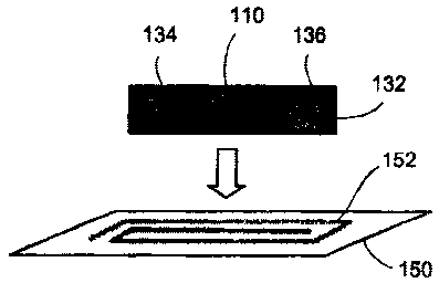
[0018] FIGS. 2A-2B show key steps in an exemplary process for manufacturing
the
present RFID tag/device having an integrated interposer.
[0019] FIGS. 3A-3H show key steps in exemplary processes for making
integrated
circuity on an interposer substrate for the present RF1D tag/device.
DETAILED DESCRIPTION OF THE PREFERRED EMBODIMENTS
[0020] Reference will now be made in detail to the preferred embodiments of
the
invention, examples of which are illustrated in the accompanying drawings.
While the
invention will be described in conjunction with the preferred embodiments, it
will be
understood that they are not intended to limit the invention to these
embodiments. On the
contrary, the invention is intended to cover alternatives, modifications and
equivalents, which
may be included within the spirit and scope of the invention as defmed by the
appended
claims. Furthermore, in the following detailed description of the present
invention, numerous
specific details are set forth in order to provide a thorough understanding of
the present
invention. However, it will be readily apparent to one skilled in the art that
the present
invention may be practiced without these specific details. In other instances,
well-known
methods, procedures, components, and circuits have not been described in
detail so as not to
unnecessarily obscure aspects of the present invention.
- 7 -
CA 02606999 2007-10-18
Docket No.: IDR0272
[0021] For the sake of convenience and simplicity, the terms "coupled
to," "connected
to," and "in communication with" mean direct or indirect coupling, connection
or
communication unless the context indicates otherwise. These terms are
generally used
interchangeably herein, but are generally given their art-recognized meanings.
Also, for
convenience and simplicity, the terms "RF," "RFID," and "identification" may
be used
interchangeably with respect to intended uses and/or functions of a device
and/or tag, and the
term "tag" or "device" may be used herein to refer to any RF and/or RFID
sensor, tag and/or
device. Also, the term "integrated circuitry" refers to a unitary structure
comprising a
plurality of electrically active devices formed from a plurality of conductor,
semiconductor
and insulator thin films, but generally does not include discrete,
mechanically attached
components (such as die, wire bonds and leads, the interposer, or an antenna
and/or inductor
component), or materials having primarily an adhesive function. In addition,
the terms
"item," "object" and "article" are used interchangeably, and wherever one such
term is used,
it also encompasses the other terms. In the present disclosure, a "major
surface" of a structure
or feature is a surface defined at least in part by the largest axis of the
structure or feature
(e.g., if the structure is round and has a radius greater than its thickness,
the radial surface[s]
is/are the major surface of the structure).
100221 The present invention concerns a RF sensor, RF surveillance
and/or RF
identification device, comprising (a) an interposer, (b) an antenna and/or
inductor on the
interposer; and (c) integrated circuitry on a surface of the interposer in a
location other than
the antenna and/or inductor, the integrated circuitry having a lowest layer in
physical contact
with the surface of the interposer. In various embodiments, the integrated
circuity comprises
thin film transistors, diodes, optional capacitors and/or resistors, and
metallization
interconnecting such circuit elements. In other embodiments, at least one
layer of the
integrated circuitry comprises a printed or laser patterned layer.
[0023] In a further aspect, the present invention concerns a method of
manufacturing
a sensor, surveillance and/or identification device, generally comprising the
steps of (1)
forming a lowest layer of integrated circuitry on a surface of an interposer;
(2) forming
successive layers of the integrated circuitry on the lowest layer of
integrated circuitry; and (3)
- 8 -
CA 02606999 2007-10-18
Docket No.: IDR0272
attaching an electrically conductive functional layer to the interposer.
Alternatively, the
method of manufacture may comprise the steps of (1) forming the lowest layer
of integrated
circuitry on the interposer surface; (2) forming successive layers of
integrated circuitry on the
lowest layer; and (3) forming an electrically conductive structure from a
functional layer
attached to the interposer. In various embodiments, one or more layers of the
integrated
circuitry are formed by printing or laser patterning the layer of material. In
one
implementation, forming the lowest layer of integrated circuitry comprises
printing or laser
patterning the lowest layer.
[0024] In an even further aspect, the present invention concerns a
method of detecting
an item or object, generally comprising the steps of (A) causing or inducing a
current in the
present surveillance and/or identification device affixed to or associated
with the item or
object sufficient for the device to radiate, reflect or modulate detectable
electromagnetic
signals; (B) detecting the detectable electromagnetic radiation; and
optionally, (C) processing
information conveyed by the detectable electromagnetic radiation. Optionally,
the method
may further comprise the step of transporting or transmitting information from
the present
device (or sensor) back to a reading device. The invention, in its various
aspects, will be
explained in greater detail below with regard to exemplary embodiments.
Exemplary MOS RFID Tags/Devices
[0025] One aspect of the invention relates to an RF identification
device, comprising
(a) an interposer; (b) an antenna and/or inductor on the interposer; and (c)
integrated circuitry
on the interposer in a location other than the antenna and/or inductor, the
integrated circuitry
having a lowest layer in physical contact with the surface of the interposer.
As a result, the
present invention provides a low-cost RFID (or EAS) tag (which may also
include sensors,
the signal modulation activities of which generally change as a result of
certain external
changes in the environment [e.g., temperature, conductivity of the structure
or surface to
which the sensor is attached, etc.], and active RFID devices; e.g., tags with
a battery on
board) comprising a substrate (e.g., an interposer), an inductor/antenna, and
an RF front end
- 9 -
CA 02606999 2007-10-18
Docket No.: IDR0272
(or subset of an RF front end and logic circuit) fully capable of operating in
accordance with
modem RFID standards.
100261 It has been shown that printed electronics based on inorganic
materials (e.g.,
laser printed nanocrystals) can be formed on certain flexible substrates, such
as high
temperature polyimides or metal foils, if a suitable thermal isolation/barrier
layer is inserted
between the substrate (e.g., the metal foil) and subsequent layers that will
be laser processed.
Thus, the present invention makes advantageous use of such materials as a
substrate or
interposer in a flexible, (at least partially) printed EAS, RF or RED tag or
device.
[00271 The interposer generally has a size that can be cost-
effectively processed using
conventional thin film processes and/or emerging or state-of-the-art printing
processes, to
produce low-cost RF circuits. Integrated circuitry can be formed on a flexible
interposer
substrate such as polyimide, glass/polymer laminate, high temperature polymer,
or metal foil,
all of which may further include one or more barrier coats. Such interposer
substrates are
generally substantially less expensive than a conventional Si die of similar
size. (However, a
conventional RFID interposer typically has a size on the order of 1 cm2 in
area, as compared
to a conventional Si RFID die, which might be about 0.01 cm2 or less in area.)
[00281 It may be advantageous to use as the interposer substrate an
anodized Al,
Al/Cu, stainless steel or similar metal foil as interconnect, electrodes and
dielectric for large
storage or IC resonance capacitors, inductors and/or as an electrode for a
diode, MOS-device
or FET, or as a WORM/OTP, deactivation or other memory storage element.
Examples of
such substrates can be found in U.S. Patent Application Nos. 10/885,283 and
11/104,375
(Attorney Docket Nos. IDR0121 and IDR0312, respectively). As a result, in many
embodiments, the antenna and/or inductor will be on a first surface of the
interposer, and the
integrated circuitry will be on a second surface of the interposer opposite
the first surface.
[0029] Thus, the invention may relate to an identification device,
comprising (a) an
interposer, (b) an antenna and/or inductor on a first surface of the
interposer; and (c)
integrated circuitry on a second surface of the interposer opposite the first
surface, the
-10-
CA 02606999 2011-11-10
Docket No.: IDR0272
(or subset of an RF front end and logic circuit) fully capable of operating in
accordance with
modern RFID standards.
[0026] It has been shown that printed electronics based on inorganic
materials (e.g., laser
printed nanocrystals) can be formed on certain flexible substrates, such as
high temperature
polyimides or metal foils, if a suitable thermal isolation/barrier layer is
inserted between the
substrate (e.g., the metal foil) and subsequent layers that will be laser
processed. Thus, the
present invention makes advantageous use of such materials as a substrate or
interposer in a
flexible, (at least partially) printed EAS, RF or RFID tag or device.
[0027] The interposer generally has a size that can be cost-
effectively processed using
conventional thin film processes and/or emerging or state-of-the-art printing
processes, to
produce low-cost RF circuits. Integrated circuitry can be formed on a flexible
interposer
substrate such as polyimide, glass/polymer laminate, high temperature polymer,
or metal foil, all
of which may further include one or more barrier coats. Such interposer
substrates are generally
substantially less expensive than a conventional Si die of similar size.
(However, a conventional
RFID interposer typically has a size on the order of 1 cm2 in area, as
compared to a conventional
Si RFID die, which might be about 0.01 cm2 or less in area.)
[0028] It may be advantageous to use as the interposer substrate an
anodized Al, Al/Cu,
stainless steel or similar metal foil as interconnect, electrodes and
dielectric for large storage or
IC resonance capacitors, inductors and/or as an electrode for a diode, MOS-
device or FET, or as
a WORM/OTP, deactivation or other memory storage element. Examples of such
substrates can
be found in U.S. Patent Application Nos. 10/885,283 and 11/104,375.
As a result, in many embodiments, the antenna and/or
inductor will be on a first surface of the interposer, and the integrated
circuitry will be on a
second surface of the interposer opposite the first surface.
[0029] Thus, the invention may relate to an identification device,
comprising (a) an
interposer, (b) an antenna and/or inductor on a first surface of the
interposer; and (c) integrated
circuitry on a second surface of the interposer opposite the first surface,
the
- 11 -
CA 02606999 2007-10-18
Docket No.: IDR0272
aluminum or stainless steel. Exemplary thicknesses depend on the material
used, but in
general, range from about 25 gm to about 200 gm (e.g., from about 50 gm to
about 100 gm).
[0032] The antenna and/or inductor may comprise the antenna, the
inductor, or both,
and may further comprise a capacitor electrode coupled thereto or integrated
therewith (see,
e.g., U.S. Patent Application Nos. 10/885,283 and 11/104,375, filed on July 6,
2004 and April
11, 2005, respectively). Generally, the antenna and/or inductor comprises a
metal. In one
embodiment, the metal may be one commercially available as a foil (e.g.,
aluminum, stainless
steel, copper, or an alloy thereof). In such cases (and where antenna and/or
inductor
components made from the metal foil, on the one hand, and the integrated
circuitry on the
other hand are on opposite sides of the interposer), the method of making a
RFID and/or EAS
device (see the following section) may further comprise the step of removing
from the metal
foil one or more portions of the metal located under (or opposite)
electrically active integrated
circuitry (e.g., transistors and diodes, but not necessarily capacitors using
a portion of the
metal foil as an electrode or plate).
[0033] In an embodiment comprising both an antenna and an inductor, the
inductor
may function as a tuning inductor (see, e.g., U.S. Patent Application No.
11/104,375). As a
result, the metal forming the antenna and inductor may not be continuous
(i.e., it may contain
an electrical disconnection), and a surveillance and/or identification device
in accordance
with the invention may comprise a first (e.g., outer) inductor coupled to a
first capacitor plate,
a second (e.g., inner) inductor coupled to a second capacitor plate, a
dielectric film on the first
(outer) inductor, the second (inner) inductor, and the first and second
capacitor plates, the first
dielectric film having openings therein exposing ends of each of the first and
second (e.g.,
outer and inner) inductors. In alternative embodiments, the capacitor plates
may be linear or
nonlinear, and/or the device may further comprise first and second nonlinear
capacitor plates
on the dielectric film, respectively coupled to the first and second linear
capacitor plates.
[0034] The present device may also further comprise a support and/or
backing layer
(not shown) on a surface of the inductor 110 opposite the dielectric film 20.
The support
and/or backing layer are conventional, and are well known in the EAS and RFED
arts (see,
- 12 -
CA 02606999 2007-10-18
Docket No.: 1DR0272
e.g., U.S. Pat. Appl. Publication No. 2002/0163434 and U.S. Pat. Nos.
5,841,350, 5,608,379
and 4,063,229). Generally, such support and/or backing layers provide (1) an
adhesive
surface for subsequent attachment or placement of the tag/device onto an
article to be tracked
or monitored, and/or (2) some mechanical support for the tag/device. For
example, the
present device may be affixed to the back of an identification label or price
tag, and an
adhesive coated or placed on the surface of the device opposite the
identification label or
price tag (optionally covered by a conventional release sheet until the label
or tag is ready for
use), to form a label or tag suitable for use in a conventional RFPD system.
Exemplary Method(s) for Making a MOS RFID Tag/Device
[0035] In one aspect, the present invention concerns a method for making an
identification device, comprising the steps of: (1) forming a lowest layer of
integrated
circuitry on an interposer; (2) forming successive layers of the integrated
circuitry on the
lowest layer of integrated circuitry; and (3) attaching an electrically
conductive functional
layer to the interposer, generally in a location other than the integrated
circuity.
Alternatively, the method of manufacture may comprise the steps of (1) forming
the lowest
layer of integrated circuitry on the interposer surface; (2) forming
successive layers of
integrated circuitry on the lowest layer, and (3) forming an electrically
conductive structure
from the interposer (e.g., when the interposer comprises an electrically
conductive material,
such as a metal foil) or a functional layer attached to the interposer (e.g.,
when the interposer
comprises a laminate of an electrically conductive material and an
electrically inactive
material, such as a metal foil having an anodized oxide film formed or grown
thereon). Thus,
the present method provides a cost-effective method for manufacturing RFID
devices.
[0036] A first exemplary method for manufacturing the present RFD)
device is
described below with reference to FIGS. 2A-2B. FIG. 2A shows tag precursor
100,
comprising interposer 132, having thereon pads 134 and 136 and integrated
circuitry 110.
Generally, integrated circuitry 110 is formed on a first major surface of
interposer 132. The
integrated circuitry 110 can be realized as a printed inorganic circuit,
largely using the
techniques described in U.S. Patent Application Nos. 10/885,283 and
11/104,375, filed on
-13-
CA 02606999 2007-10-18
Docket No.: IDR0272
July 6, 2004 and April 11, 2005, respectively. Exemplary steps in forming
"bottom gate"
devices using this approach are described below and are depicted in partial
cross-section in
FIGS. 3A-3H.
[0037] Thereafter, pads 134 and 136 are formed on the same surface of
interposer 132
[0038] Next, holes or vias may be formed in the major surface of
interposer 132
opposite that on which pads 134 and 136 and integrated circuity 110 have been
formed.
Generally, and referring now to FIG. 2A, there is one hole or via through
interposer 132
exposing a surface of pads 134 and 136 and enabling electrical connection to a
terminal of
[0039] The process described here can result in a lower overall tag
cost by reducing
the number of expensive/low throughput attachment steps, as well as reducing
the cost of
fabricating the active electronics. A low cost tag may be produced by directly
printing or
-14-
CA 02606999 2007-10-18
Docket No.: IDR0272
otherwise forming the circuitry on an interposer that is then relatively
cheaply attached at
relatively low accuracy to an inductor/carrier. This may be advantageous where
the
processing of the circuitry may be performed on a flexible substrate such as
polyimide,
glass/polymer laminate, high temperature polymer, or metal, all of which may
further include
one or more barrier coats.
100401 The interposer is generally of a size that enables cost-
effective manufacturing
using conventional thin film processes, as well as conventional and/or state-
of-the-art printing
processes, to produce low-cost RF circuits. These processes include
sputtering, evaporation,
LPCVD, PECVD, bath etching, dry etching, direct laser printing of device
elements, ink jet
printing of any element or layer, spray coating, blade coating, extrusion
coating,
photolithography, printed etch mask lithography of any layer (such as laser or
inkjet), offset
printing, gravure printing, embossing, contact printing, screen printing,
combinations thereof,
and/or other techniques. Nearly any layer of material in the integrated
circuitry of the present
invention can be made by essentially any of these techniques. In particular,
the present
invention enables low-cost manufacturing of RFID and/or EAS tags by low-cost
process
technologies, such as printing or a combination of printing and conventional
display (e.g., flat
panel display) processing. In the latter case, use of the interposer as a
substrate for
manufacturing integrated circuitry enables a decrease in the effective area
onto which active
materials may be blanket-deposited (e.g., by CVD) and/or processed by
equipment/processes
conventionally used to make the integrated circuitry. Thus, the present method
may further
comprise the step of forming one or more second layers of the integrated
circuitry by
conventional display processing, for example.
[0041] As will become apparent from the following description, in the
present
invention, the antenna and/or inductor can be formed on the same side or on
opposite sides of
the interposer. Also, equipment that processes continuous roll- or spool web-
based substrates
can be used to make the present integrated circuitry on the interposer (as
well as to attach the
antenna/inductor structure, in those embodiments in which the antenna and/or
inductor are
attached to the interposer after making the integrated circuitry).
- 15 -
CA 02606999 2007-10-18
Docket No.: IDR0272
Exemplary Method(s) for Making Integrated Circuitry
[0042] Generally, integrated circuitry is formed directly on a fast
major surface of
interposer 132. For "top gate" type devices with integrated capacitors and
diodes, the
integrated circuitry 110 can be realized as a (partially) printed,
substantially inorganic circuit,
using the techniques described in U.S. Patent Application Nos. 11/084,448,
11/203,563, and
11/452,108, filed on March 18, 2005, August 11, 2005, and June 12, 2006,
respectively.
[0043] Exemplary steps in forming "bottom gate" devices are described
below and are
depicted in partial cross-section in FIGS. 3A-3H. Many of the techniques
described below
(although not necessarily used to make bottom gate devices) are also described
in U.S. Patent
Application Nos. 11/084,448, 10/885,283, and 11/104,375, filed on March 18,
2005, July 6,
2004, and April 11, 2005, respectively.
Prepare Interposer Substrate
[0044] Referring now to FIG. 3A, the interposer substrate 210 may
comprise any
flexible or inflexible, electrically active or insulative substrate capable of
(i) providing
physical support for the integrated circuitry formed thereon during formation
thereof and for
the RF transmitter/receiver components attached thereto during attachment
thereof, (ii)
having integrated circuitry formed (preferably printed) thereon, and (iii)
enabling electrical
connections to be formed therethrough (i.e., so that signals can be
transmitted between
integrated circuitry formed on one major surface of the interposer and the RF
receiver/transmitter components attached to the opposite major surface of the
interposer).
The interposer 210 may thus comprise a metal foil (preferably, with a
dielectric film [which
may be anodized] thereon), polyimide, thin glass, or inorganic/organic
laminate substrate.
[0045] Preferably, the interposer substrate 210 is conventionally
cleaned and coated
with a barrier material 220 (such as silicon dioxide or aluminum oxide) before
further
processing. The coating step may comprise oxidation and/or anodization of a
surface
material of the interposer substrate (e.g., a metal foil), deposition of spin-
on or fluid coated
barrier films (Honeywell AcuGlass series or others), sputtering, CVD, or spray
coating a
- 16 -
CA 02606999 2007-10-18
Docket No.: IDR0272
barrier material onto the interposer substrate, or a combination of any of
these processes. As
shown in FIG. 3A, the barrier material 220a-b coats at least two major
surfaces of the
interposer 210. Optionally, the surface of at least one barrier material layer
(e.g., 220a) may
be treated (e.g., roughened, activated, etc.) and/or cleaned prior to the next
step. To the extent
the interposer comprises a metal sheet or foil, the metal foil may be etched
and/or cut as
described in U.S. Patent Application Nos. 10/885,283, 11/104,375 and
11/452,108, filed on
July 6, 2004, April 11, 2005, and June 12, 2006, respectively, to isolate the
contact pads for
the antenna.
Gate and Gate Laver Interconnect Formation
[0046] Referring now to FIG. 38, a gate metal layer 230 may be
conventionally
sputtered onto barrier material layer 220a. The gate metal layer 230 may
comprise any metal
conventionally used in integrated circuits and/or printed circuitry, such as
aluminum,
titanium, tantalum, chromium, molybdenum, tungsten, iron, cobalt, rhodium,
iridium, nickel,
palladium, platinum, copper, silver, gold, zinc, etc., or alloy thereof, such
as aluminum-
titanium, aluminum-copper, aluminum-silicon, molybdenum-tungsten, titanium-
tungsten,
etc., or electrically active (e.g., conductive) compound thereof, such as
titanium nitride,
titanium silicide, tantalum nitride, tantalum silicide, molybdenum nitride,
molybdenum
silicide, tungsten nitride, tungsten silicide, cobalt silicide, etc. Gate
metal layer 230 may have
a conventional thickness (e.g., of from 50 nm to 5000 nm, preferably from 80
nm to 3000 rim,
more preferably from 100 nm to 2500 urn, or any range of thicknesses therein).
[0047] Thereafter a resist may be deposited thereon. The resist may
comprise a
conventional photoresist or a thermal resist, and may be conventionally
deposited or formed
on gate metal layer 230 (e.g., spin coating or ink jetting). Conventional
photolithography or
print/pattern lithography by laser irradiation may be performed (e.g.,
selectively irradiating
portions of the resist, then developing the resist [selectively removing
irradiated or non-
irradiated portions of the resist, depending on whether the resist is positive
or negative] with a
conventional developer, see, e.g., U.S. Patent Application No. 11/203,563,
filed on August
11, 2005) to leave a patterned resist 235 that defmes the gates, as shown in
FIG. 313, and gate-
- 17 -
CA 02606999 2007-10-18
Docket No.: IDR0272
level interconnects (not shown, but which may take the form of a conventional
"landing pad"
located outside the cell or active area of a transistor or other circuit
component formed from
gate metal layer 230). The exposed gate metal 230 is then etched, and the
patterned resist 235
stripped, to form gates (e.g., 232 and 234 as shown in FIG. 3C) and gate-level
interconnects.
Alternatively, the gate layer 230 may be deposited and patterned by printing
(e.g., inkjetting)
of a metal precursor ink and subsequent curing, and/or laser patterning of a
metal precursor
layer (which may include both direct conversion [e.g., laser-induced direct
conversion to
metal] and indirect conversion [e.g., laser-induced crosslinlcing of metal-
containing species
and subsequent annealing to form a conductive metal film]).
Form Gate Dielectric
[0048] Referring now to FIG. 3D, a gate dielectric layer 240
(comprising, e.g., a
nitride and/or oxide of silicon, aluminum, etc.) is formed over the gates and
gate-level
interconnects 232 and 234 by sputtering, C'VD or other blanket deposition
process. Gate
dielectric layer 240 may have a thickness of from 10 rim to 100 mm, preferably
from 10 rim to
50 rim, more preferably from 10 nm to 40 nm, or any range of values therein.
[0049] Alternatively, gate dielectric layer 240 may be printed (e.g.,
by ink jetting or
other printing process described in U.S. Patent Application Nos. 10/885,283
and/or
11/104,375) over the gates and gate-level interconnects 232 and 234.
Appropriate film
properties and/or qualities (e.g., thickness, density, dielectric constant,
etc.) may be provided
by printing and subsequently processing a plurality of layers. Such subsequent
processing
may comprise oxidizing a printed dielectric precursor material (such as
nanoparticles of
silicon and/or aluminum), densifying the dielectric material, doping the
dielectric material,
etc.
[0050] In a further alternative, a gate dielectric layer may be formed
from gate-level
metal structures 232 and/or 234 by direct, conventional thermal or
electrochemical (e.g.,
anodic) oxidation of gate metal 232 and/or 234. One or more of the gate-level
metal
- 18 -
CA 02606999 2007-10-18
Docket No.: IDR0272
structures may be conventionally masked (e.g., with a photo- or laser-
patternable resist) if a
dielectric film is not desired thereon.
Form Semiconductor Laver(s)
100511 Thereafter, as shown in FIG. 3D, a semiconductor layer 250
(which may
comprise intrinsic or lightly doped Si) may be sputtered, coated or otherwise
blanket
deposited (e.g., by CVD) over the gate dielectric layer 240. Semiconductor
layer 250 may
have a thickness of from 80 urn to 2000 urn, preferably from 100 inn to 1500
urn, more
preferably from 150 mu to 1000 urn, or any range of values therein.
Semiconductor layer
250, which may be patterned by conventional photolithography or laser
patterning (see, e.g.,
U.S. Patent Application No. 11/203,563, filed on August 11, 2005), may
function generally as
a transistor channel.
[00521 Optionally, a contact layer may be formed on semiconductor
(channel) layer
250 by conventional masking and ion implantation, or by sputtering, coating or
otherwise
blanket depositing (e.g., by CVD) a heavily doped Si (source/drain) contact
layer onto
semiconductor layer 250. Then, if the source/drain contact layer is blanket
deposited, source
and drain contact structures 252a and 252b may be formed by conventional
planarization
(e.g., polishing [chemical-mechanical polishing], or deposition of a thermally
planarizable
material such as a resist and non-selective etch back), and silicon islands
may be formed by
conventional photolithography, laser irradiation of thermal resists or printed
(e.g., ink jetted)
resist lithography patterning, followed by dry or wet etching and resist
stripping. Portion(s)
255 of the heavily doped Si layer over the gate may be either not formed
(e.g., not printed) or
removed (e.g., by photolithography and etching, or by forming layer 252 as an
amorphous
layer, then not laser irradiating [e.g., crystallizing] that portion and
removing the non-
irradiated portion by etching it selectively to the crystallized silicon)
prior to subsequent
processing.
100531 Alternatively, and also as shown in FIG. 3E, semiconductor
layer 250 and
heavily doped Si contact layer 252a-b may be printed from a semiconductor
(e.g., doped or
-19-
CA 02606999 2007-10-18
Docket No.: IDR0272
undoped silane) ink in locations corresponding to the silicon islands; see,
e.g., U.S. Patent
Application Nos. 10/789,317, 10/950,373, 10/949,013, 10/956,714, and
11/246,014, filed on
February 27, 2004, September 24, 2004, September 24, 2004, October 1, 2004,
October 8,
2004, and October 6, 2005, respectively. Generally, semiconductor layer 250 is
printed and
subsequently processed before heavily doped Si contact layer 252a-b (i.e.,
without the portion
255 above the gate) is printed thereon. After printing, the ink is dried,
cured and/or annealed
to change its morphology (e.g., at least partially crystallize the dried ink).
Annealing or laser
irradiation may also activate some or all of the dopant therein. Printing not
only increases
throughput by avoiding resist deposition and removal steps, but also enables
direct formation
of discrete source and drain contact layers 252a and 252b.
Form Interlayer Dielectric and Vias
[0054]
Formation of the interlayer dielectric and vias from the semiconductor and
gate layers is largely conventional. For example, as shown in FIG. 3F, a
relatively thick
dielectric layer 260 may be deposited onto semiconductor layer 250 (and, if
present, contact
layer 252), then vias 262 may be formed by conventional photolithography,
laser irradiation
of thermal resists or printed resist lithography patterning, followed by a
conventional
dielectric etch. Alternatively, a patterned dielectric layer 260 (e.g., with
vias 262 formed
therein) may be printed onto semiconductor layer 250 (e.g., by inkjetting, as
explained above
with regard to the gate dielectric layer 240). Interlayer dielectric 260 may
have a thickness,
for example, of at least 0.5 pm, and preferably from 1 to 25 pm, 2 to 10 pm,
or any range of
values therein.
Form Source/Drain (S/Diand Interlayer Interconnects
10055] If
heavily doped semiconductor layer 252a-b has not been formed (see, e.g.,
FIG. 3E), S/D layer 270 may be sputtered, coated or otherwise blanket
deposited onto
interlayer dielectric 260 and into vias 262. Typically, S/D layer 270
comprises a heavily
doped semiconductor material, similar to heavily doped semiconductor layer
252a-b. S/D
layer 270 may have a thickness, for example, of from 20 nm to 1000 urn,
preferably from 40
nm to 500 urn, more preferably from 50 nm to 100 urn, or any range of values
therein.
-20 -
CA 02606999 2007-10-18
Docket No.: IDR0272
100561 Referring now
to FIG. 3G, interconnect metal 280 may be sputtered, coated or
otherwise blanket deposited onto S/D layer 270 (including into vias 262).
Interconnect metal
280 generally comprises a metal, alloy or electrically active compound,
similar to gate metal
230, and may have a thickness, for example, of from 0.5 to 10 Fun., preferably
from 0.75 to 8
pm, and more preferably from 1 to 5 pm, or any range of values therein. Since
interconnect
metal 280 may contact a silicon-containing layer, interconnect metal 280 may
further
comprise a lower silicon barrier layer (e.g., a metal nitride, such as TIN).
100571 Conventional
photolithography, laser irradiation of a thermal resist or ink jet
resist patterning of the blanket-deposited S/D and interlayer interconnect
layers defines the
S/D regions and interlayer interconnects, and conventional metal (and
semiconductor) etching
forms the actual interconnects. Similar connections may be formed to
predetermined
locations along the gate metal, but preferably in a location other than (e.g.,
outside of) the
silicon islands 255 (see, e.g., FIG. 3E).
[0058] Alternatively,
and as shown in FIG. 3H, S/D structures 272-278 may be
printed from a semiconductor (e.g., doped or undoped silane) ink in locations
corresponding
to vias 262 (see, e.g., U.S. Patent Application Nos. 10/885,283 and/or
11/104,375). If an
undoped ink is used, the process for forming S/D structures 272-278 may
further comprise a
doping step (e.g., comprising conventional ion implantation or ion shower
doping).
Thereafter, interconnect metal structures 280 may be formed as described
above, with the
addition of lower adhesive and/or silicon barrier layers, if desired.
100591 After
formation of the integrated circuitry is substantially complete, the
present method may further comprise the step of passivating the integrated
circuitry and/or
the device (e.g., forming a passivation or dielectric layer over the
integrated circuitry and, to
the extent they may be exposed, portions of the interposer or substrate). The
passivation layer
generally inhibits or prevents the ingress of water, oxygen, and/or other
species that could
cause the degradation or failure of the integrated circuitry or device, and
may add some
mechanical support to the device, particularly during further processing. The
passivation
layer may be formed by conventionally coating the upper surface of the
integrated circuitry
-21-
CA 02606999 2007-10-18
Docket No.: IDR0272
and/or device with one or more inorganic barrier layers such as a
polysiloxane; a nitride,
oxide and/or oxynitride of silicon and/or aluminum; and/or one or more organic
barrier layers
such as parylene, a fluorinated organic polymer, or other barrier material.
Alternatively, the
passivation layer may further comprise an underlying dielectric layer, which
may comprise a
material having lower stress than the overlying passivation layer. For
example, the dielectric
layer may comprise an oxide, such as Si02 (e.g., CVD TEOS), USG, FSG, BPSG,
etc., and
the passivation layer may comprise silicon nitride or a silicon oxynitride.
Also, the
passivation layer may have a thickness slightly greater than that of the
dielectric layer.
[0060] At this point in the processing (or at any point where a
further material
providing some physical or mechanical support to the integrated circuitry or
device is added),
the mechanical or physical support function of the interposer is no longer
necessary. As a
result, parts of the interposer supporting the integrated circuitry can be
removed entirely (e.g.,
in the case where the interposer is generally electrically insulating) or in
part (e.g.õ in the case
where the interposer is electrically conducting, such as a metal foil, in
which case the
remaining parts of the interposer may form an antenna, one or more inductors,
and/or wire
electrically connecting the antenna and/or inductor to a via or contact
through the [remaining]
interposer to the integrated circuitry or a separate wire thereto). In such a
ease, the interposer
in the final device, tag or sensor may be a dielectric film or other insulator
formed on the
same surface of the metal foil on which the integrated circuitry is formed.
Hybrid Integrated Circuitry
[0061] Alternatively, the tag precursor (e.g., interposer 132 in FIG.
2A having
integrated circuitry 110 and pads 132-134 thereon) could take a "hybrid" form.
For example,
it may be advantageous to combine a printed, inorganic semiconductor- and/or
conductor-
based RI "front end" in conjunction with a relatively inexpensive, easily
fabricated, relatively
high functionality organic or 'conventional Si chip based (digital) logic
and/or memory circuit.
The term "RF front end" refers to the inductors, capacitors, diodes, and FETs
that operate at
or near the carrier frequency and/or that modulate that frequency, and is
shown lby the "IC"
area 110 in FIGS. 2A-2B. These elements (and circuit blocks comprising or
consisting
- 22 -
CA 02606999 2007-10-18
Docket No.: IDR0272
essentially of such elements) are generally analog in nature (e.g., they
function and/or operate
in an analog or continuous manner), and may require higher performance devices
than the
relatively slow, digital logic circuit.
100621 This
"hybrid" form may be a particularly advantageous combination in the
case of organic circuitry, which may possess certain advantages in terms of
cost of materials
and/or manufacture. Organic circuitry may be suitable for the controller,
logic and/or
memory sections of the circuit, which often operate at frequencies
significantly lower than the
RF frequency (e.g., at 1 MHz or lower). However, organic FET circuitry may not
be able to
operate effectively at the carrier frequency (e.g., about 13.56 MHz or
higher). For example,
the design and manufacture of diodes having the desired rectification, leakage
and breakdown
characteristics based on organic materials have some documented challenges. It
may also be
difficult to realize effective organic modulation FETs or organic clock-
related FETs that
operate at the carrier RF frequency. In this case, a hybrid circuit comprising
an RE front end
as disclosed herein and that is fabricated from high performance printed
inorganics, and an
organic logic and/or memory circuit which could be fabricated directly on to
the RF front end
(which would act as the underlying substrate or carrier), may be
manufacturable.
[0063] As a
result, the present invention relates to a method of making an
identification device or tag, comprising (1) forming a lowest layer of
integrated circuitry on a
first surface of an interposer; (2) forming successive layers of the
integrated circuitry on the
lowest layer of integrated circuitry; and (3) attaching an electrically
conductive functional
layer to a second surface of the interposer opposite the first surface. The
present invention
therefore enables a low-cost process for producing an RFID (or EAS) tag
comprising a
substrate, an RF front end or subset of an RF front end and logic circuit.
An Exemplary Method of Reading the Present RFID Tags
100641 The present invention further relates to method of detecting an item
or object
in a detection zone comprising the steps of: (a) causing or inducing a current
in the present
device sufficient for the device to radiate detectable electromagnetic
radiation (preferably at a
- 23 -
CA 02606999 2007-10-18
Docket No.: IDR0272
frequency that is an integer multiple or an integer divisor of an applied
electromagnetic field),
(b) detecting the detectable electromagnetic radiation, and optionally, (c)
processing
information conveyed by the detectable electromagnetic radiation. Generally,
currents and
voltages are induced in the present device sufficient for the device to
radiate detectable
electromagnetic radiation when the device is in a detection zone comprising an
oscillating
electromagnetic field. This oscillating electromagnetic field is produced or
generated by
conventional EAS and/or RFID equipment and/or systems. Thus, the present
method of use
may further comprise the step of (d) transporting or transmitting information
from the present
device (or sensor) back to a reading device, or (prior to step (a)) attaching
or affixing the
present device to an object or article (e.g., an identification card,
packaging for goods to be
shipped, etc.) to be detected, or otherwise including the present device in
such an object,
article or packaging therefor.
[0065] The present tags are designed at least in part to work with
electronic
identification and/or security systems that sense disturbances in radio
frequency (RF)
electromagnetic fields. Such electronic systems generally establish an
electromagnetic field
in a controlled area, defined by portals through which articles must pass in
leaving the
controlled premises (e.g., a retail store, library, etc.) or a space in which
the article must be
placed to be read and identified. A tag having a resonant circuit is attached
to each such
article, and the presence of the tag circuit in the controlled area is sensed
by a receiving
system that detects the tag and processes information obtained therefrom
(e.g., determines
unauthorized removal of an article or the identity of goods in a container
labeled with the
tag). Most of the tags that operate on these principles are single-use or
disposable tags, and
are therefore designed to be produced at low cost in very large volumes.
100661 Alternatively, the present tag may take the form of a sensor,
the RF signal
modulation characteristics and/or properties of which may change as the
characteristics
and/or properties of the object or article to which it is attached change. For
example, the
present sensor may be attached to a stainless steel (or other metal) object,
structure or surface.
As the properties of the object, structure or surface change (e.g., the steel
oxidizes, a metal
- 24 -
CA 02606999 2007-10-18
Docket No.: IDR0272
having electromagnetic properties becomes magnetized or carries a minimum
threshold
electrical current, or the object or surface [regardless of its composition]
changes temperature
by a predetermined difference or a threshold amount), the characteristics
and/or properties of
the RF signal radiated, reflected or modulated by the present sensor also
change in a
detectable manner.
100671 The present tags may be used (and, if desired and/or
applicable, re-used) in any
commercial LAS and/or RFID application and in essentially any frequency range
for such
applications. For example, the present tags may be used at the frequencies,
and in the fields
and/or ranges, described in the Table below:
Preferred
Frequencies
Rangeeld
Preferred Range/Field of Exemplary Commercial
of Detection/
Frequencies Response Detection/ Application(s)
Response
100-150 125-134 KHz up to 10 feet up to 5 feet animal ID, car
anti-theft
KHz
systems, beer keg tracking
5-15 MHz 8.2 MHz, 9.5 up to 10 feet up to 5 feet inventory
tacking (e.g.,
MHz, 13.56 libraries, apparel, auto/
MHz
motorcycle parts), building
security/access
800-1000 868-928 MHz up to 30 feet up to 18 feet pallet and shipping
container
MHz
tracicing, shipyard container
tracking
2.4-2.5 GHz about 2.45 GHz up to 30 feet up to 20 feet auto toll tags
Table 1. Exemplary applications.
[0068] The present invention thus also pertains to article
surveillance techniques
wherein electromagnetic waves are transmitted into an area of the premises
being protected at
a fundamental frequency (e.g., 13.56 MHz), and the unauthorized presence of
articles in the
area is sensed by reception and detection of electromagnetic radiation emitted
by the present
- 25 -
CA 02606999 2007-10-18
Docket No.: IDR0272
device 100. This emitted electromagnetic radiation may comprise second
harmonic or
subsequent harmonic frequency waves reradiated from sensor-emitter elements,
labels, or
films comprising the present device that have been attached to or embedded in
the articles,
under circumstances in which the labels or films have not been deactivated or
otherwise
CONCLUSION / SUMMARY
[0069] Thus, the present invention provides a MOS identification
device having an
integrated interposer, and methods for its manufacture and use. The
identification device
generally comprises (a) an interposer, (b) an antenna and/or inductor on a
first surface of the
[0070] Novel elements of the invention may include (i) direct
integration of circuit
manufacturing/processing steps onto an interposer substrate and/or (ii)
printing directly onto
-26-
CA 02606999 2007-10-18
Docket No.: IDR0272
an interposer carrier, which is then inexpensively attached to an inductor
formed on or from a
low cost substrate material such as metal foil. In one embodiment, the
inductor has a larger
area (and thus may have two greater dimensions) than the interposer. Such
direct
manufacturing/ processing steps are compatible with web, continuous, roll-to-
roll and/or
sheet processing and with conventional flexible, thin RF labels, and should
provide an
increased throughput in the tag manufacturing process. Fabrication of circuit
elements
directly on an interposer enables low cost manufacturing, as the resolution of
the pick and
place process for assembling the interposer and inductor/antenna is low. The
inventive
approach enables the efficient/low cost use of device substrate materials
which are thermally
and chemically compatible with RF1D and/or EAS tag manufacturing and/or that
provide
appropriate barrier properties, but which otherwise might be too expensive if
used for the
interposer substrate of an entire tag.
[0071] The foregoing descriptions of specific embodiments of the
present invention
have been presented for puiposes of illustration and description. They are not
intended to be
exhaustive or to limit the invention to the precise forms disclosed, and
obviously many
modifications and variations are possible in light of the above teaching. The
embodiments
were chosen and described in order to best explain the principles of the
invention and its
practical application, to thereby enable others skilled in the art to best
utilize the invention
and various embodiments with various modifications as are suited to the
particular use
contemplated. It is intended that the scope of the invention be defined by the
Claims
appended hereto and their equivalents.
-27-