Note: Descriptions are shown in the official language in which they were submitted.
CA 02607364 2011-09-19
METHOD AND APPARATUS FOR CONTROLLING A SEMICONDUCTOR
OPTICAL AMPLIFIER FOR USE IN A PASSIVE OPTICAL NETWORK
Field of the Invention
[001] The present invention relates to a method and apparatus for controlling
a
semiconductor optical amplifier for use in a passive optical network, and more
specifically,
to a method and apparatus for maintaining the gain of the semiconductor
optical amplifier at
predetermined level during normal operation of the passive optical network.
Background of the Invention
[002] Various current communication systems utilize passive optical network
(PON)
technology. Network operators presently utilize PONs to provide broadband
communications services, such as data, subscription television and telephony,
to homes and
small businesses. Such PON systems typically can support a maximum optical
fiber reach
of 20 km (i.e., from the central office to the subscriber), and a maximum
"split ratio" of 32
subscribers per feeder fiber. These limits are due to limitations in optical
transmitter power
output and optical receiver sensitivity in commercially available components.
One way to
extend the reach and increase the split ratio of a PON is to use optical
amplifiers to
compensate for the additional fiber and optical splitter losses. It is noted
that the invention
discussed below focuses on Gigabit-capable PON (GPON), ITU-T Recommendation
G.984.
However, it is also applicable to other PON technologies, including but not
limited to,
Broadband PON (BPON, ITU-T Recommendation G.983) and Gigabit Ethernet PON
(GEPON, IEEE 802.3ah).
[003] Existing PONs typically operate on a wavelength plan of approximately
1490
nun in the downstream direction, and 1310 nm in the upstream direction. In
order to use the
same wavelength band for extended range and/or larger split ratio,
semiconductor optical
1
CA 02607364 2011-09-19
amplifiers (SOAs) are presently a primary cost effective technology which can
be designed
for use in 1490 nm and 1310 nm wavelength band.
[004] An SOA typically has an approximately 40 rim useable waveband. The
standardized downstream GPON waveband is in the range of 1480 nm to 1500 rim,
or about
20 tun wide. For upstream transmission, the current GPON standards specify a
waveband
of 1260 nm to 1360 nm, or about 100 nm wide. Typical upstream lasers actually
operate at
around 1310 rim, with a waveband which is about 20 nm to 30 nm wide. In order
to reduce
the SOA's amplified spontaneous emission (ASE) noise contribution to the
upstream signal
quality, the upstream signal band should be limited to about 20 rim, such as
from 1300 nm
to 1320 nm, e.g., using a coarse wavelength division multiplexed (CWDM) laser.
[005] Fig. 1 illustrates a typical amplified PON system 10. Referring to Fig.
1, the
system includes an optical network unit (ONU) 12, a lxN optical coupler 14 (as
a variation,
2xN optical couplers are utilized in protected PON designs), a first
wavelength division
multiplexer (WDM) 16 and a second wavelength division multiplexer 18, which
are coupled
to a first SOA 20 and a second SOA 22. In the given embodiment, the first SOA
20
amplifies signals propagating in the downstream direction, and the second SOA
22
amplifies signals propagating in the upstream direction. The system 10 further
includes an
optical line terminator OLT, which is located in the central office. As shown,
the OLT
includes a transmitter 26, a receiver 28, and a WDM 32, which couples both the
transmitter
26 and the receiver 28 to the feeder fiber.
[006] With respect to the operation, when an ONU 12 has data to send, and
further
has received a transmission grant as defined in the PON protocol, the ONU 12
sends a burst
of data in the upstream direction, through one (or more) SOA 22 to the OLT in
the central
office. The amplified PON 10 has a plurality of ONUs 12 coupled to the first
SOA 22 and
feeder fiber by the N-port optical coupler 14. Thus, in the upstream
direction, the coupler
2
CA 02607364 2011-09-19
14 combines the output signals from the ONUs 12, and couples the combined
signal to the
input of the first upstream SOA 22, by way of the WDM filter 16. The received
power level
at the upstream SOA 22 may vary between ONUs 12, due, e.g., to differences in
the lengths
of distribution fibers and to variations in ONU transmitter output power.
Thus, the
upstream input signal at the SOA 22 will have wide dynamic range over
timescales of the
order of 1 s to 10s of s or more.
[007] Optical amplifiers, such as SOAs, are typically designed to be either
constant
gain or constant power amplifiers. In the PON application, the downstream SOA
20 may be
either constant gain or constant power. However, for the upstream SOA 22,
constant gain
operation is necessary due to differences in input signal level from the
different ONUs 12,
and the use of burst mode operation for transmitting data in the upstream
direction.
[008] It is well known that semiconductor devices experience permanent changes
in
their crystalline structure over time and use, which affects their
performance. Due to this
aging effect, SOA gain will drift over time. Thus, proper means to monitor and
compensate
for gain variation must be implemented. However, measurement of gain of
upstream SOA
22 with sufficient accuracy to monitor and compensate for aging is made
difficult by the
dynamic range of the upstream input signal.
[009] Accordingly, there is a need for an effective, cost sensitive method and
apparatus for controlling the gain of SOA's utilized in the upstream direction
in PON
applications, which at the same time could provide for an optical supervisory
channel for
communication between the central office (CO) and a remote node. It is an
object of the
present invention to provide a method and apparatus which achieves these
objectives.
3
CA 02607364 2011-09-19
Summary of the Invention
[010] Accordingly, the present invention relates to a system and method for
maintaining the gain of a semiconductor optical amplifier at a predetermined
level during
the normal operation of the device, even when the device is processing burst
data in the
upstream direction.
[011] More specifically, the present invention relates to an optical amplifier
including: an amplifier having an input port and an output port, which is
disposed along a
main signal line of the optical amplifier; a dummy laser generation circuit
having an output
coupled to the main signal line and operative for inputting a dummy signal
into the
amplifier; a first optical detector for detecting a power level of the dummy
signal into the
amplifier and outputting a first power level signal; a second optical detector
for detecting an
amplified power level of the dummy signal output by the amplifier and
outputting a second
power level signal; a memory device for storing calibration data regarding the
gain
characteristics of the amplifier; and a gain control circuit which receives
inputs from the
first optical detector and second optical detector, and has an output coupled
to the amplifier.
The gain control circuit calculates the gain of the SOA based on the first
power level signal,
the second power level signal and the calibration data. The gain control
circuit further forms
a feedback loop which operates upon the calculated gain to maintain said gain
at a
predetermined level, e.g. by adjusting the drive current into the SOA.
[012] The present invention also relates to a method for controlling the gain
of an
optical amplifier. The method includes the steps of storing calibration data
regarding the
gain characteristics of the amplifier in a memory device, e.g., during
assembly; coupling a
dummy signal onto a main signal line of the optical amplifier, and inputting
the dummy
signal into an amplifier, where the dummy signal is coupled with an upstream
data signal
prior to being input into the amplifier; detecting a power level of the dummy
signal input
4
CA 02607364 2011-09-19
into the amplifier and outputting a first power level signal; detecting an
amplified power
level of the dummy signal output by the amplifier and outputting a second
power level
signal; and controlling the gain of the amplifier based on the first power
level signal, the
second power level signal and the calibration data such that the gain of the
amplifier is
maintained at a predetermined level during operation of the optical amplifier.
[013] The present invention provides significant advantages over the prior art
systems. Most importantly, the present invention provides a PON network
utilizing an SOA
that provides for the processing of upstream burst data signals while
maintaining the gain of
the SOA at a predetermined level despite device aging, utilizing a simple,
cost effective
circuit.
[014] Additional advantages of the present invention will become apparent to
those
skilled in the art from the following detailed description of exemplary
embodiments of the
present invention.
[015] The invention itself, together with further objects and advantages, can
be
better understood by reference to the following detailed description and the
accompanying
drawings.
Brief Description of the Drawings
[016] The following drawings serve to illustrate the principles of the
invention.
[017] Fig. I illustrates an exemplary prior art PON design.
[018] Fig. 2 illustrates a prior art SOA configuration.
[019] Fig. 3 illustrates an exemplary burst data signal input into the SOA.
[020] Fig. 4 illustrates an exemplary embodiment of an SOA control circuit in
accordance with the present invention.
[021] Fig. 5 illustrates an exemplary gain profile of an SOA.
5
CA 02607364 2011-09-19
[022] Fig. 6 illustrates another exemplary embodiment of the present
invention.
[023] Fig. 7 illustrates an exemplary embodiment regarding the use of a single
dummy laser in conjunction with multiple SOAs.
[024] Fig. 8 illustrates another exemplary embodiment of the present
invention,
which allows for the use of the dummy laser signal for monitoring purposes.
Detailed Description of the Preferred Embodiments
[025] Prior to discussing the present invention, a brief discussion of prior
art
techniques for controlling optical amplifiers, such as SOAs and erbium-doped
fiber
amplifiers (EDFA), is provided to facilitate an understanding of the present
invention. Fig.
2 illustrates an exemplary prior art approach for controlling optical
amplifiers in a typical
fiber communications application. Referring to Fig. 2, the photo detector 31
at the input
measures the input optical signal level via coupler 33, and photo detector 32
at the output of
the optical amplifier 25 measures the output optical signal via coupler 34. An
amplifier
control circuit 35 utilizes these measured optical signal levels to determine
the gain of the
optical amplifier 25. The amplifier control circuit 35 further utilizes a
feedback control
circuit to control the optical amplifier to attempt to maintain either
constant gain or constant
output power. In prior art systems, optical amplifiers are designed to deal
with nearly
constant average optical signals, as produced by point-to-point transmission
systems such as
SONET or Ethernet. Since the average optical input signal level to the optical
amplifier 25
is nearly constant, relatively slow optical detectors 31 and 32 can be
utilized to measure the
optical signal average power. However, the signal level of the PON upstream
optical signal
varies from burst to burst, depending upon which ONUs sent the signal.
Therefore, the
traditional control scheme shown in Fig. 2 used for controlling optical
amplifiers is not
suitable for controlling an upstream amplifier in a PON application.
6
CA 02607364 2011-09-19
[026] Fig. 3 illustrates an example of the wide dynamic signal level at the
input of
the upstream SOA 25 and the varying duration of upstream bursts. These
variations in the
input signal level makes it difficult to design a control circuit that
accurately compares the
input signal with the output signal, resulting in inaccurate reading of the
SOA gain. As
such, as noted above and shown in Fig. 2, a feedback loop is necessary to
monitor input and
output levels of the SOA so as to measure gain and to allow for the adjustment
of drive
current to maintain a pre-determined level. Furthermore, as an SOA ages, the
SOA
typically requires higher drive current to maintain its pre-determined gain
setting. It is
noted that an alarm may be generated when the drive current exceeds a pre-
determined
threshold, to indicate that the SOA is close to end-of-life. Thus, input and
output optical
signal power levels to the SOA must be accurately measured despite the dynamic
range and
varying duration of optical bursts at the input to the SOA.
[027] As explained in detail below, the present invention relates to a method
and
apparatus which is capable of maintaining the gain and output power level of
the SOA at the
desired level, notwithstanding the variations in the input signal level, due
to, for example,
burst mode operation, and aging of various components, such as the SOA and the
ONU
components. It is noted that the present invention is particularly applicable
to the upstream
signal path of the PON, as the upstream mode of operation allows for a burst
mode (the
downstream signal is typically continuous and from a single source).
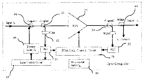
[028] Fig. 4 illustrates an exemplary embodiment of an SOA circuit 40 of the
present invention. The SOA circuit 40 contains the same basic configuration as
the SOA
circuit illustrated in Fig. 2 (which are indicated by the same reference
numerals), but
includes the following additional components. Referring to Fig. 4, the
additional
components include a laser control unit 47 which is coupled to a dummy laser
46. The
dummy laser 46 is coupled to the main signal line by coupler 44. Further, a
WDM filter 43
7
CA 02607364 2011-09-19
is coupled between coupler 33 and the first optical detector 31. The output of
first optical
detector 31 is also coupled to the laser control circuit 47. Continuing a non-
volatile
memory 45 is coupled to an SOA gain control circuit 36. Finally, a WDM filter
37 is
coupled between coupler 34 and the optical detector 32, and another WDM filter
49 is
disposed on the main signal line at the output of the device.
[029] With regard to the operation of the exemplary embodiment shown in Fig.
4, a
signal from the dummy laser 46 is coupled into the SOA 25 input port, along
with the
upstream optical input signal, by utilizing the first optical coupler 44. It
is noted that the
first optical coupler 44 may be, for example, a power coupler or a wave
division
multiplexing (WDM) filter. The dummy laser 46 has a wavelength X d, which is
outside the
upstream PON waveband, but within the SOA 25 gain spectrum. The second optical
coupler 33 taps a portion of the combined optical signal, and the tapped
signal then passes
through the WDM optical signal filter 43, which operates to pass the signal at
k d, while
rejecting the upstream burst optical signal. The output of the WDM optical
signal filter 43
is coupled to the first optical detector 31. The first optical detector 31
operates to measure
the dummy signal. As explained in further detail below, the dummy signal, as
measured by
the first optical detector 31, is utilized as the reference for the SOA 25
input level.
[030] At the output port of the SOA 25, the third optical coupler 34 utilized
to tap a
small portion of the combined amplified optical signal. The second optical WDM
filter 37
is utilized to block the upstream burst PON signal, while passing the
amplified dummy
signal. The second optical detector 32 operates to detect the amplified dummy
signal, and
the signal level at the second optical detector 32 is utilized as a reference
for the SOA
output. The output of the third optical coupler 34 may be coupled to an
additional optical
WDM filter 49, which blocks the amplified dummy laser signal and only passes
the
amplified upstream burst PON optical signal toward the OLT.
8
CA 02607364 2011-09-19
[031 ] It is noted that the inclusion of the dumping WDM filter 49 in the
circuit
configuration is optional. For example, if multiple SOAs are needed in an
amplified PON
design, the dummy signal can be allowed to propagate with the burst signal to
the next
SOA, which does not need to have its own dummy laser. Further, the dummy laser
may
also be modulated for use in a simplex communications channel, as will be
described further
below.
[032] Referring again to Fig. 4, in the given embodiment, the dummy laser 46
generates an unmodulated continuous wave (CW) signal. As such, the signals as
measured
at the first optical detector 31 and the second optical detector 32 are highly
stable and can be
used to calibrate the gain setting of the SOA 25. It is noted that standard
calibration
procedures for calibrating the SOA 25 can be utilized. Once the calibration
process is
completed, the relative signal levels measured at first optical detector 31
and the second
optical detector 32 can be utilized to calculate the SOA gain value as
follows. If the light
incident on first optical detector 31 results in a photocurrent Il and the
light incident on
second optical detector 32 results in photocurrent 12, the overall gain G for
the SOA 25
(including the upstream PON signal) is defined by equation 1, which is:
G=a(I2111)......... Eq.(1),
where a is the calibration value, which is a constant and is does not change
with SOA gain.
The calibration constant a is stored in the non-volatile memory 45 once the
calibration
process is completed. Then, during operation, the SOA gain control circuit 36,
which is
coupled to first optical detector 31 and the second optical detector 32, and
to non-volatile
memory 45, operates to control the bias applied to the SOA 25 so as to
maintain a constant
gain of the SOA 25 during the operation of the device, in accordance with the
relationship
defined by equation 1.
9
CA 02607364 2011-09-19
[032] As discussed above, the upstream PON optical signal should have an
optical
wavelength range of 20 nm to 30 nm. An SOA typically has approximately 45 urn
of gain
bandwidth with relatively flat gain over this gain bandwidth (i.e., a
variation of about 3 dB).
Further, the SOA gain profile typically does not change much during operation.
Therefore,
maintaining a constant SOA gain at the dummy laser wavelength )j will ensure
that the gain
at the PON wavelength of the upstream signal is also kept constant.
[033] In the given embodiment, because the dummy laser 46 is used only for
measurement purposes, it is preferable that the dummy laser have a lower power
level (e.g., a
few dB lower) than the power level of lowest upstream PON optical signal
anticipated at the
input to the optical amplifier 25. As a result, the dummy laser signal will
have a negligible
effect on the operation of SOA 25 operation. Fig. 5 illustrates the SOA gain
profile as well as
possible wavelengths of the upstream PON optical signal and dummy laser signal
relative to
the gain profile. Fig. 5 illustrates that the dummy laser wavelength, Xd, must
be separated
from the upstream PON signal range, but must also be within the SOA gain
spectrum
window.
[034] Thus, as a result of the configuration of the foregoing embodiment,
since the
dummy laser signal, rather than the upstream burst PON optical signal, is used
to control the
SOA gain, the SOA gain may be accurately set with a relatively simple control
circuit.
[035] It is noted that commercially available SOAs may not provide sufficient
gain
for all amplified PON applications. If more gain is necessary, a two-stage
amplifier,
incorporating a cascade of two or more SOAs, can be utilized. In such a case,
a second
exemplary embodiment of the present invention can be utilized to control both
stages of the
SOAs with a single dummy laser. Fig. 6 illustrates an exemplary circuit
configuration of the
second embodiment of the present invention. Referring to Fig. 6, in addition
to the
components contained in the first embodiment, the circuit includes a second
SOA 61, which
CA 02607364 2011-09-19
receives the output of coupler 34, an optical coupler 62, which taps a portion
of the output of
a second SOA. This signal is coupled into an optical WDM filter 63, which
blocks the
upstream burst signal and passes the amplified dummy laser signal. The output
of the WDM
filter 63 is provided to an optical detector 64, which measures the amplified
dummy laser
signal. Then, in the same manner as discussed above with the first embodiment
regarding the
first amplifier stage 25, the relative signal levels measured at the optical
detector 32 and the
optical detector 64, after initial calibration, can be used to calculate the
gain of the second
stage SOA 61 in the following manner. If the light incident on optical
detector 32 results in
photocurrent 12 and the light incident on optical detector 64 results in
photocurrent 13, the
overall gain G' for the second stage SOA 61 (including the upstream PON
signal) is defined
by equation 2, which is:
G' = a' (13/12) ......... Eq. (2),
where a' is the calibration value for the second SOA 61, which is typically
not equal to a, the
calibration value for the first SOA 25. The calibration value, a', is also
stored in the non-
volatile memory 45 at the completion of the calibration process. During
operation, the SOA
gain control circuit 36, which is coupled to optical detectors 32 and 64, and
to the non-
volatile memory 45, controls the bias applied to the second SOA 61 so as to
maintain a
constant gain of the second SOA 61 defined by the relationship set forth in
equation (2). Of
course, in this embodiment, the SOA gain control circuit 36 also provides
feedback control of
the first SOA 25, as in the first embodiment. Thus, the gain of both the first
stage and second
stage SOAs gain can be independently controlled using the same dummy laser
signal.
[036] Fig. 7 illustrates an exemplary optical power splitter 69 coupled at its
input to
the dummy laser 46, and at its outputs to a plurality of WDM filters or
optical couplers.
These in turn are coupled to the main signal line via the WDM filter or
coupler and fed to the
11
CA 02607364 2011-09-19
SOA amplifiers in the same manner as in the first embodiment illustrated in
Fig. 4. Fig. 7
illustrates how a single dummy laser signal can be coupled to multiple SOAs.
[037] Fig. 8 illustrates an exemplary configuration which allows the use of
the
dummy laser signal for telemetry purposes. Specifically, Fig. 8 shows the
additional
components that allow for the foregoing function, and which can be added to
any of the
foregoing embodiments. It is noted that only the components of the previous
configurations
necessary to facilitate understanding of the operation of this embodiment, and
the required
additional components are illustrated in Fig. 8. Referring to Fig. 8, the
device includes one or
more sensors 71, which operate to monitor the values of operational parameters
of the SOA;
an element management agent device 72, which may be implemented utilizing a
microcontroller, and which operates to collect data from the sensors 71, and
to format this
received data into messages; a transmitter 73 which operates to place the
messages formed by
the element management agent 72 into a data packet of a pre-determined format,
for example,
but not limited to Ethernet frames, serialize the message and transmit the
messages as a bit
stream at a pre-determined clock rate; and a coupler device 74 operative for
combining the
message data output by the transmitter 73 with the output of the laser control
circuit 47, such
that the gain of the dummy laser 46 is modulated when the transmitter 73 is
active. At the
OLT, the monitoring system further includes a WDM filter 75 which operates to
extract the
modulated signal from the dummy laser from the aggregate upstream signal. The
modulated
signal is then detected by a photodetector 76 and recovered and formatted into
data packets
by the receiver 77. An element manager unit 78 processes the messages in the
data packets
for further use in managing the SOA and the operation thereof, as well as the
PON. Receiver
77 and element manager 78 may be coupled by way of a data communications
network, e.g.,
a local area network, which is not illustrated for simplicity purposes.
12
CA 02607364 2011-09-19
[038] The processes described in connection with Figs. 4-8 may be implemented
in
hard wired devices, firmware or software running in a processor. A processing
unit for a
software or firmware implementation is preferably contained in the laser
control circuit 47 or
also in-part in the SOA gain control circuit 36. Any of these processes may be
contained on
a computer readable medium which may be read by laser control circuit 47 or
also in-part in
the SOA gain control circuit 36. A computer readable medium may be any medium
capable
of carrying instructions to be performed by a microprocessor, including a CD
disc, DVD disc,
magnetic or optical disc, tape, silicon based removable or non-removable
memory,
packetized or non-packetized wireline or wireless transmission signals.
[039] Those of skill in the art will appreciate that a computer readable
medium may
carry instructions for a computer to perform a method of controlling the power
level input
into an optical amplifier, the method comprising at least the steps of:
detecting the power
level of a burst signal to be input to an amplifier circuit of the optical
amplifier, the burst
signal being detected at an input port of said optical amplifier; coupling a
dummy laser
generation signal to the input port of the optical amplifier; and controlling
the power level of
a signal output by the dummy laser generation circuit so as to maintain the
power level of a
signal formed by the combination of said burst signal and the dummy laser
generation signal
at a substantially constant level, the combination signal being input to the
amplifier circuit.
The instructions may further include coupling at least a portion of said burst
signal to a gain
control circuit which is operative for controlling the power level of the
signal output by said
dummy laser generation circuit; coupling the output of the dummy laser
generation circuit
with the burst signal so as to form the combination signal; and coupling at
least a portion of
the combination signal to the gain control circuit.
[040] The present invention provides significant advantages over the prior art
systems. Most importantly, the present invention provides a PON network that
provides for
13
CA 02607364 2011-09-19
the processing of upstream burst data signals while maintaining the gain of
the SOA
at a predetermined level utilizing a simple, cost effective circuit.
[041] The present invention also provides additional advantages over the
prior art devices. More specifically, in addition to those already noted
above, the
present invention may assist in fault sectionalization if the OLT experiences
a
reduction in upstream optical power, or loss of upstream optical signal. As
the dummy
laser is isolated from the passive splitter, distribution fibers and drop
fibers of the
PON network, utilizing the dummy laser signal, it can easily be determined
whether
the SOA is functional by measuring the gain of the SOA. If the SOA is
functional, the
problem must be in the fiber plant between the optical amplifier and
subscribers. On
the other hand, if the SOA gain is not in its nominal range, it can be
confirmed that
the problem lies with the SOA, and a technician cannot be dispatched to
replace it.
Without the dummy laser signal to control the SOA in the manner disclosed by
the
present invention, there is no way to distinguish between such faults.
[042] The scope of the claims should not be limited by the preferred
embodiments set forth in the examples, but should be given the broadest
interpretation
consistent with the description as a whole.
14