Note: Descriptions are shown in the official language in which they were submitted.
CA 02608456 2007-10-29
SIT002BCA
Title: Automatic device for the ignition and control of a gas apparatus
and relative driving method
DESCRIPTION
Field of application
The present invention relates to an automatic device for the ignition and
control of a gas apparatus equipped with at least one burner and with
electrically controlled valve means for regulating the flow of gas from a
main pipe towards a nozzle associated with said at least one burner.
The automatic device being supplied by at least one supply voltage
provided by the electricity main and/or by battery means, being coupled
to a ground terminal and comprising:
- a spark circuit suitable for generating a pilot flame upon receipt a start
signal.
ls The present invention also relates to a driving method of an automatic
device for the ignition and control of a gas apparatus.
The invention concerns, in particular but not exclusively, a device for gas
apparatuses like for example fires, stoves and gas braziers and the
following description refers to this field of application with the sole
purpose of simplifying its explanation.
- 1-
CA 02608456 2007-10-29
SIT002BCA
Prior art
As known, gas fireplaces, gas stoves and gas braziers are ignited
activated by an electromechanical ignition device, generally activated by
a user, which allows the ignition of a pilot flame at a pilot burner as well
as its supervision to ensure that the pilot flame acts as an ignition source
for a burner of greater thermal power.
There are suitable valve means for regulating the gas coupled with the
ignition device, arranged between the main pipe for the gas and the
burners, which are subjected to a thermocouple.
1o The thermocouple, heated by the flame of the burner,
electromechanically monitors the permanent ignition state of the flame.
Therefore, possible flame extinction determines a cooling down of the
thermocouple and, consequently, the closure of the gas supply to the
burner.
In such apparatuses, it is easy to verify if the flame has been
extinguished or lost, since it is generally due to a gust of air, a jump in
the flue draft, a simple exhaustion of the gas or similar anomalies.
Therefore the flame needs to be constantly monitored in the burner in
order to avoid damaging and dangerous gas leaks. The
2 o electromechanical monitoring, by thermocouple, although advantageous
from various points of view, has the drawback that the gas supply is not
shut off immediately but occurs only after the cooling of the
thermocouple itself. Therefore, there is a danger of the gas escaping
- 2-
CA 02608456 2007-10-29
SIT0026CA
without being burnt for a certain period of time before being intercepted.
Moreover, during the initial flame ignition step the user has to perform a
direct manual action in the vicinity of the burner to keep the flame active
for a time necessary to heat up the thermocouple. This manual action is
risky for the user.
In order to avoid these drawbacks, in recently apparatuses the
thermocouples are regulated by special devices that automatically check
for the presence of a flame during the ignition step of the gas
apparatuses.
Such automatic devices are also supplied by electricity main and by
battery means or buffer batteries allowing the apparatuses on which they
are installed to operate when the electricity main is not feeding.
Usually the apparatuses, like for example gas fires, are used at locations
where there is not a constant supply of electrical power, but rather varies
unpredictably.
Automatic devices with thermocouple are substantially high energy
consumption devices since they require a high current to maintain the
main flow of gas, during the automatic ignition step, to support the flow of
gas during the heating step of the thermocouple, and for possible
2 o restoring after a flame has been lost.
Therefore, due to the high power required, automatic devices with
thermocouple, supplied by buffer batteries, have very low autonomy and
are therefore not very efficient, requiring continuous replacement of the
- 3-
CA 02608456 2007-10-29
SIT002BCA
batteries by the user.
This represents a limitation to use of such automatic devices in gas
apparatuses.
One aim of the present invention is that of providing an automatic device
for gas apparatuses, having structural and functional characteristics such
as to overcoming the limits and/or drawbacks with reference to devices
realised according to the prior art to be overcome.
Another aim of the present invention is to provide an automatic device
with low energy consumption in order to dynamically biasing the valve
means.
Summary of the invention
One aspect of the present invention is directed to an automatic device
for the ignition and control of a gas apparatus comprising at least one
burner for regulating the flow of gas from a main pipe towards a nozzle
associated with said at least one burner;
- a spark circuit suitable for generating a pilot flame upon receipt a
electric start signal;
- electrically controlled valve means associated to said at least one
burner;- at least one supply voltage provided by the electricity main
2 o and/or by battery means, to supply said automatic device
- an electrical microprocessor unit in said automatic device to drive and
to control said valve means and said spark circuit;
- 4-
CA 02608456 2007-10-29
SIT002BCA
- at least one actuator circuit activated by said electrical microprocessor
unit through an activation signal having a pulse train to dynamically bias
said valve means and to regulate its charge state according to the duty
cycle of the pulse train.
The main advantage of the automatic device according to the invention
is that it is substantially a low-voltage device with low power
consumption, with electrical and completely independent management in
terms of the initial ignition step, in terms of the control of the valve means
and for the supervision of the flame. Moreover, such a device, when
lo there are anomalies, allows the completely automatic restoring of the
device to be carried out unexpectedly quickly, or else allows it to be
made safe.
Another aspect of the present invention is directed to a method for
driving an automatic device for the ignition and control of a gas
apparatus equipped with at least one burner and including electrically
controlled valve means for regulating the gas flow from a main pipe
towards a nozzle associated with said at least one burner;
said automatic device being supplied by at least one supply voltage
provided by the electricity main and/or by battery means and being
coupled to an ground terminal,
said method comprising the following steps:
- initial automatic ignition phase activating a spark circuit upon receipt of
a start signal to generate a flame in said at least one burner;
- 5-
CA 02608456 2007-10-29
SIT002BCA
- driving and controlling said valve means and said spark circuit through
an electrical microprocessor unit;
- activating at least one actuator circuit coupled to said valve means by
means of an activation signal having a pulse train generated by said
electrical micorprocessor unit;
- activating at least one actuator circuit coupled to said valve means by
means of an activation signal generated by said electrical unit, said
activation signal having a pulse train to dynamically charge said valve
means for an activation time period defined by the duty cycle of the pulse
train.
The main advantage of the method for driving the automatic device
according to the invention is its efficiency linked to the low energy
consumption required and the completely electrical management in
terms of the ignition step, for the flame control step and during the
operation of the device; moreover, such a method, when there are
anomalies, allows the automatic device to be automatically restored or
be made safe quickly.
The characteristics and advantages of the automatic device according to
the present invention will be apparent from the following description of an
2 o example embodiment thereof, by way of an embodiment thereof given by
way of indicative and not limiting example with reference to the annexed
drawings.
Brief description of the drawings
- 6-
CA 02608456 2007-10-29
SIT002BCA
In such drawings:
- figure 1 schematically shows an apparatus of an automatic device for
ignition and control, according to the invention;
- figure 2 schematically shows a block diagram of the apparatus of figure
1;
- figure 3 is a block diagram of the device according to the present
invention;
- figures 4-15 show details of the blocks as shown in figure 3;
- figures 16-18 show an actuator circuit of the valve means, made
io according to the invention, in the various operating steps;
- figure 19 shows a diagram with a time progression of an activation
signal of the actuator circuit according to the present invention;
- figures 20-21 show a time reference circuit associated with an electrical
unit and made according to the invention, in two operating steps;
- figure 22 shows a diagram with time sequences of operating signal
relative to the circuit of figure 20;
- figure 23 illustrates a diagram with time progressions of operating
signal relative to a flame detector made according to the present
invention.
2 o Detailed description
With reference to such figures an automatic device made according to
- 7-
CA 02608456 2007-10-29
SIT002BCA
the present invention for the ignition and control of a gas apparatus 1 is
globally and schematically indicated with 10.
The gas apparatus 1 is in particular a gas fireplace, schematically
represented in figure 1, but the automatic device 10 can be used in other
apparatuses like for example gas stoves and gas braziers and similar.
The gas apparatus 1 is equipped with a pilot burner 11 and with a main
burner 12 and suitable electrically controlled valve means 7, for
regulating the flow of gas from a main pipe 28 for the gas towards a first
nozzle 8, coupled with the pilot burner 11 and to a second nozzle 13,
coupled with the main burner 12, respectively.
The pilot burner 11 and the main burner 12 are coupled in the usual way,
so that the flame at the pilot burner 11 can act as ignition source for the
gas released by the nozzle 13 to the main burner 12. Advantageously, a
supply voltage provided by electricity main 2, through a transformer 3,
and by battery pack 4 supplies the automatic device 10; the automatic
device 10 is coupled through a ground terminal 59 to a constant
reference voltage GND that in the present embodiment is a ground
voltage.
Moreover, the valve means 7 are supplied by a supply voltage and are of
the type with the valve normally closed.
In particular, the valve means 7 comprise a first solenoid 17, which
actuates a first shutter associated with the first nozzle 8 so that when the
solenoid is crossed by an electric current the first shutter opens allowing
- 8-
CA 02608456 2007-10-29
SIT002BCA
the gas to flow, whereas, when the solenoid is not crossed by an electric
current the shutter closes blocking the flow of gas.
Similarly, a second solenoid 18 actuates a second shutter associated
with the second nozzle 13.
The automatic device 10 comprises a spark circuit 80 suitable for
generating a flame on the pilot burner 11, close to the first nozzle 8,
upon receipt of a start signal Start.
According to the present invention, the automatic device 10 comprises
an electrical microprocessor unit 5 that actuates and electrically controls
lo both the spark circuit 80 and such valve means 7, so as to uniformly and
totally burn all of the gas put out exploiting to the highest degree the
thermal value as well as in complete safety.
Advantageously, according to the present invention the valve means 7
are activated by the electrical unit 5 and are coupled to the ground
terminal 59.
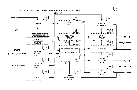
The automatic device 10, as illustrated in figure 4, comprises a first
actuator circuit 40 and a second actuator circuit 45, structurally similar,
dynamically activated by the electrical unit 5, through a first activation
signal 21 and a second activation signal 22, respectively.
Advantageously, the first activation signal 21 and the second activation
signal 22 are signals having a pulse train with a predetermined charge
factor or duty cycle.
- 9-
CA 02608456 2007-10-29
SIT002BCA
Such actuator circuits 40, 45 are suitable for dynamically polarising the
valve means 7 to regulate its charge state according to the duty cycle of
the pulse train.
In particular, according to the present invention, the automatic device 10
and in particular the electrical unit 5 is substantially a circuit operating
at
low voltage that dynamically drives such valve means 7, with a low power
consumption and a substantial saving of energy.
The automatic device 10 is supplied by:
- the electricity main 2 that supplies a voltage VAC to the transformer
rectifier 3, which through a first terminal 16 provides a first supply
voltage VDC; and
- battery pack 4 that supply a second supply voltage VBB through a
second terminal 20.
According to an embodiment, the transformer rectifier 3 comprises a
Graetz bridge rectifier or else a modern switching voltage regulator, for
example of the Step-Down or Buck type.
A remote control panel 6 allows the electrical unit 5 to be activated upon
receipt of the start signal Start. The start signal Start is transmitted
through a set of terminals 27 and can consist of a protocol, in the form of
an encoded signal, or else the reading of a switch or contact open and
closed state.
According to an embodiment, the remote control panel 6 comprises a
- 10-
CA 02608456 2007-10-29
SIT002BCA
pair of switches coupled to the array of terminals 27.
A diagnostic circuit 14 interacts with the electrical unit 5 through suitable
connection terminals 15 and allows the user to keep the automatic
device 10 constantly under remote observation, allowing possible
anomalies to be diagnosed.
According to the present invention, in the case of anomalies the
automatic device 10 acts autonomously intervening to restore its
functionality or to place it under safe conditions.
The control panel 6 and the diagnostic circuit 14 could in some cases be
lo incorporated directly in the electrical unit 5.
In particular, the electrical unit 5 comprises a programmable
microcontroller 30 capable of storing a management programme that
analyses the received signals, generating suitable signals for the
operation and for the safety of the automatic device 10 itself.
The automatic device 10 also comprises a selector 50 that is supplied in
input by the first supply voltage VDC and by the second supply voltage
VBB to supply in output a third constant voltage VCC_Pos, which is
substantially the greater of the input supply voltages.
Advantageously, as shall be specified hereafter, the selector 50 uses the
2 o battery pack4 as a buffer battery both in the case of a total lack of the
first supply voltage VDC, and in the case in which the electricity main 2
supplies sporadic low voltages compared to a nominal voltage.
- 11-
CA 02608456 2007-10-29
SIT002BCA
In particular, the selector 50 feeds an enable circuit 46, a regulator circuit
60 and a high voltage generator circuit 85.
The enable circuit 46 provides in output a fourth voltage VCC which is a
voltage substantially translated in level compared to the third voltage
VCC_Pos and suitable for feeding the first 40 and the second actuator
circuit 45 and defined arranged control peripherals.
The regulation circuit 60 carries out a first filtering for possible over
voltages in the third supply voltage VCC_Pos supplying in output a
substantially stabilised fifth supply voltage VDD suitable for feeding the
lo electrical unit 5.
Advantageously, according to the present invention, as highlighted in
figure 4, the first actuator circuit 40 and the second actuator circuit 45
are supplied by the fourth supply voltage VCC respectively through a first
supply terminal 47 and a second supply terminal 48 and they are also
coupled to the ground terminal 59. Moreover, they are activated by the
first activation signal 21 and by the second activation signal 22 received,
respectively, at a first input terminal 23 and at a second input terminal
24.
Advantageously, the first activation signal 21 and the second activation
signal 22 having a pulse train have regular pulses of rectangular wave
shape with a particular and predetermined charge factor or duty cycle, so
as to dynamically activate the valve means 7 coupled to a respective
output terminal 34, 35.
- 12-
CA 02608456 2007-10-29
SIT002BCA
In particular, according to a preferred embodiment, the first actuator
circuit 40 comprises a first inductance L1, arranged between the first
supply terminal 47 and an inner node A, a first capacitance C1, arranged
between the inner node A and an output node E, which is coupled with
the ground terminal 59 through a first diode D1 that, for greater
efficiency, is of the Schottky type.
A first resistance R33 is also arranged between the output node E and
the first output terminal 34.
A first switch Q1 is arranged between the inner node A and the ground
terminal 59 and is suitably activated at a command terminal G by the first
activation signal 21.
The first switch Q1 can be a Fet or Mosfet transistor or else a BJT
transistor.
A first resistive divider R7-R8 is coupled with the first input terminal 23
and is coupled to the ground terminal 59 and allows the voltage of the
first activation signal 21 to be adjusted in a predetermined way.
Furthermore, the first actuator circuit 40 comprises a first filtering
element Fl arranged between the inner node A and the ground terminal
59 capable of filtering the signal present at the inner node A. In
particular, the first filtering element Fl comprises, coupled in series, a
resistance R4 coupled to the inner node A and to a capacitance C9.
!n a preferred embodiment, at the first actuator circuit 40 a Zener diode
DZ3 is arranged between the inner node B and the command terminal G
- 13-
CA 02608456 2007-10-29
SIT002BCA
of the first switch Q1, to make a further protection of the first actuator
circuit 40 against over voltages that could reach the fourth supply voltage
VCC through the first supply terminal 47.
Advantageously, the first impulsive activation signal 21, based upon the
provided duty cycle, has an activation time period TON and a deactivation
time period TOFF and dynamically biases the first inductance L1 and the
first capacitance C1. In particular, the first actuator circuit 40 absorbs
electrical energy discontinuously from the fourth supply voltage VCC only
during the activation time period TON and returns it by taking a
lo substantially continuous current from such valve means 7.
The first activation signal 21 generates a potential at the output node E
that is kept below the potentials of the other nodes of the first actuator
circuit 40. In particular, the potential of the output node E is less than the
ground voltage GND of the ground terminal 59.
Advantageously, the activation time period TON of the first activation
signal 21 is substantially less than the deactivation time period TOFF.
In other words, unlike the prior art, the first actuator circuit 40:
- during the activation time period TON, receives a charge current, i.e.
from the first solenoid 17, keeping the flow of gas to the first burner 11
open;
- during the deactivation time period TOFF, the output node E is coupled
to the ground terminal 59 through the first diode D1 and thus also the
first solenoid 17 and the first solenoid 17 as a effect of its own
- 14-
CA 02608456 2007-10-29
SIT002BCA
inductance is crossed by a current still coming out towards the output
terminal E, keeping the flow of gas to the first burner 11 open.
This allows, in particular, the energy required by the first actuator circuit
40 during its operation to been substantially reduced with a substantial
reduction of the power absorbed.
With reference to figure 19, the duty cycle of the first activation signal 21
is defined by the formula:
duty cycle = ToN/(ToN+ToFF)
where TON is the activation time period and TOFF is the deactivation time
period.
With reference to figures 16-18, the operation of the first actuator circuit
40 is analysed in particular.
Figure 16 shows the first actuator circuit 40 in a rest state, in which the
fourth supply voltage VCC is present whereas the first activation signal
21 is absent, i.e. the electrical unit 5 enables the enable circuit 46 but
still
does not command the first actuator circuit 40.
In this case, the first switch Q1 is in open state and the first capacitance
Cl is charged at the fourth supply voltage VCC through a current that,
from the first supply terminal 47 slips through the first inductance L1, the
first capacitance Cl and the first diode Dl towards the ground terminal
59.
Figures 17 and 18 illustrate the first actuator circuit 40 activated by the
- 15-
CA 02608456 2007-10-29
SIT002BCA
first activation signal 21, in a first and a second operative condition,
respectively.
In particular, in the first operative condition, the first activation signal
21
is active for the activation time period TON and the first switch Q1 closes
connecting the inner node A to the ground terminal 59. The first
inductance L1 accumulates inductive energy, whereas the first
capacitance C1 discharges absorbing current from the first solenoid 17
whilst the first diode D1 is electrically blocked.
In such a first operative condition, for the brief activation time period TON,
1o the first actuator circuit 40 absorbs a current from the first solenoid 17
and in particular a current slips from the charge towards the inner node A
making the voltage at the output node E negative with respect to the
reference voltage GND present at the ground terminal 59.
In such a first operative condition, the first solenoid 17, crossed by the
electric current, allows the first shutter to open allowing the gas to flow to
the pilot burner 11, whereas the power required by the first actuator
circuit 40 is given by the energy accumulated by the first inductance L1
during the brief activation time period TON.
In the second operative condition, the first switch Q1 is kept open for the
passive time period TOFF. The first inductance L1 discharges the
inductive energy accumulated during the activation time period ToN,
recharging the first capacitance C1 through the first diode D1 which is
also brought into conduction and a current continues to flow from the first
solenoid 17 to the first diode Dl.
- 16-
CA 02608456 2007-10-29
SIT002BCA
Therefore, also during the deactivation time period TOFF, the output node
E is kept at a negative voltage with respect to the reference voltage GND
of the ground terminal 59. The first solenoid 17, crossed by substantially
continuous current, allows the first shutter to be kept open allowing the
gas to flow to the pilot burner 11 without any power requirement from the
supply and therefore with a substantial saving of energy.
Substantially, therefore, the first actuator circuit 40 activated by the first
activation signal 21 keeps the transfer of energy from the to the charge
operative with a transfer factor that depends upon the duty cycle of the
first activation signal 21.
Furthermore, when the first activation signal 21 is deactivated the first
switch Q1 is kept open and the first actuator circuit 40 is taken back into
rest state.
Moreover, advantageously, according to the present invention, the first
activation signal 21 has the duty cycle regulated so that the current that
crosses the first solenoid 17 for each activation time period TON and for
each deactivation time period TOFF, is greater than a minimum opening
current suitable for keeping the first shutter open making the gas flow to
the pilot burner 11.
Advantageously, according to the present invention, the electrical unit 5
modulates the duty cycle of the first activation signal 21 according to
some parameters, like for example:
- value of the fifth supply voltage VCC;
- 17-
CA 02608456 2007-10-29
SIT002BCA
- value of the minimum opening current of the first solenoid 17;
- value of a temperature of the first solenoid 17, as shall become clearer
hereafter.
In particular, there is substantially a retroaction between the first actuator
circuit 40 and the electrical unit 5. A value of the measured current
I_Measure, proportional to the current present at the first output terminal
34, is detected through a detection terminal 31 coupled to the first output
node E.
Such a value is suitably processed by the electrical unit 5 based upon
suitable reference values stored and possible corrective compensations
of the duty cycle of the first activation signal 21 can be foreseen, in
relation to the specific parameters of the first solenoid 17, indicated
above. This allows a substantial saving of energy at the automatic circuit
10.
Moreover, in the case in which the first solenoid 17 undergoes variations
due to the environment temperature that can change the electrical
characteristics, for example such as to generate undesired deactivation
thereof, the value of the measured current I_Measure undergoes
variations which are intercepted by the electrical unit 5 and are
compensated correctively by varying the duty cycle of the first activation
signal 21.
Similarly, as highlighted in figure 4, the second actuator circuit 45
comprises a second inductance L2 arranged between the second supply
- 18-
CA 02608456 2007-10-29
SIT002BCA
terminal 48 and an inner node A', a second capacitance C2 arranged
between the inner node A' and an output node E' which is coupled with
the ground terminal 59 through a second Schottky diode D2. A second
resistance R72 is coupled in series between the output node E' and
through a second output terminal 35 to the charge or else to the second
solenoid 18.
A second switch Q3, arranged between the inner node A' and the ground
terminal 59, is driven dynamically by the second activation signal 22
which is suitably regulated in voltage by a second divider R12-R14.
In a preferred embodiment, the second actuator circuit 45 has a Zener
diode DZ6 that is arranged between the inner node B' and the command
terminal G' of the second switch Q3, to make a further protection against
excessive voltages that could reach the fourth supply voltage VCC
through the terminal 48.
The second impulsive activation signal 22, based upon the provided duty
cycle, regulates a charge time ToN, and a discharging time TOFF' of the
second capacitance C2 keeping the second output node E' at a potential
that is less than any potential present at the other nodes of the second
actuator circuit 45 and in particular of the voltage at the ground terminal
2 o 59.
A second filtering element F2 is arranged between the inner node A' and
the ground terminal 59 allowing the signal to be filtered at the inner node
A' and has, coupled in series, a resistance R12 and a capacitance C19.
- 19-
CA 02608456 2007-10-29
SIT002BCA
Similarly to the first actuator circuit 40, the second actuator circuit 45
biases the second solenoid 18 in relation to the duty signal of the second
activation signal 22, providing, in particular, a current to the actuator
circuit 40 during the charge time period TON'.
This allows a low energy consumption improving the performance of the
automatic device 10 itself.
Furthermore, the first actuator circuit 40 and the second actuator circuit
45 to satisfy defined control and safety regulations can, instead of a first
capacitance Cl and a second capacitance C2, have many capacitances
lo Cl', C2', C3' and C10, C11 and C12, respectively, arranged in series
and placed between the respective inner node A and A' and the output
node E and E' as highlighted in figure 4.
Similarly, the first actuator circuit 40 and the second actuator circuit 45 to
increase efficiency of energy conversion can, as an alternative to the first
diode Dl and the second diode D2, have two or more diodes, D3 and
D4, as well as D5 and D6, respectively, arranged in parallel and coupled
between the output node E, E' and the ground terminal 59. Such diodes
can, in some cases, be Schottky diodes.
It is worth noting that the first resistance R33 and the second resistance
2 o R72, in series respectively with the output nodes E, E', could be replaced
by a pair of inductances of a value similar to the first and second
inductance L1 and L2, without for this reason jeopardising the operation
of the actuator circuits 40 and 45, as well as of the automatic device 10.
Therefore, it is possible to improve the attenuation of possible
- 20-
CA 02608456 2007-10-29
SIT002BCA
interferences conducted from and towards the nodes E, E' at the first
drive signal 41 and at the second drive signal 42, also allowing current
specific regulations to be respected, like for example the regulations
known by the acronym EMC (Electro-Magnetic Compatibility).
Furthermore, the diode DZ3 and the diode DZ6 may not be present
without for this reason jeopardising the operation of the actuator circuits
40 and 45, as well as of the automatic device 10.
Moreover, according to the present embodiment there is advantageously
retroaction between the first actuator circuit 40 and the electrical unit 5.
According to the present embodiment, the automatic device 10
comprises an unique connector CN1, shown repeatedly in figures 4, 6
and 13, which represents a unitary and main connection interface
between the electrical unit 5 and the peripherals of the automatic device
10, allowing quick and easy connection.
is In particular, the connector CN1 receives the first supply voltage VDC
through the first terminal 16 and the second supply voltage VBB through
the second terminal 20, and it is suitably coupled to the ground terminal
59.
In particular, the connector CN1 has three successive terminals that
contact a command reading circuit 100, shown in figure 13, which
receives respective signals 101, 103 coming through the set of terminals
27 from the command panel 6. Such signals 101, 103 are interpreted by
the microcontroller 30 so as to generate the activation signal for the
enable circuit 46 for driving the first actuator circuit 40 and the second
- 21-
CA 02608456 2007-10-29
SIT002BCA
actuator circuit 45.
Finally, the connector CN1 has three further terminals that contact the
valve means 7 respectively coupling the output terminals 34, 35 and the
ground reference terminal 59 of the first 40 and of the second actuator
circuit 45, to respective terminals 41 and 42 of the first solenoid 17 and
of the second solenoid 18.
Even more specifically, a fourth input terminal of the connector CN1 is
arranged to receive a switching signal Command_Switch, a fifth input
terminal of the connector CN1 is arranged to receive a selection signal
Mode_switch and a sixth terminal of the connector CN1 is arranged to
receive the return signal Switch_GND provided by the connection with
the set of terminals 27 towards a command panel 6.
The selector 50, illustrated in figure 6, receives, in particular through the
connector CN1, the first supply voltage VDC and the second supply
voltage VBB respectively at a second input terminal 51 and at a first
input terminal 52, and it is coupled to the ground terminal 59 to supply, to
an output terminal, the third supply voltage VCC_Pos. In particular, the
third supply voltage VCC_Pos is the maximum voltage between the input
supply voltages. According to an embodiment, the selector 50 comprises
a first diode D12, in series with the first input terminal 51, and a second
diode D13, in series with the second input terminal 52, as well as a filter
F3 suitably coupled in series with the first diode D12 and with the second
diode D13 and coupled to the output terminal 56.
Advantageously, the first diode D12 and the second diode D13 are of the
- 22-
CA 02608456 2007-10-29
SIT002BCA
Schottky type and in particular go into blocking mode in the presence of
possible inverse voltages at the respective input terminals, blocking the
passage of current.
The first filter F3 comprises a first capacitance C8, a first inductance L6
and a second inductance L7 and attenuates possible interferences
conducted, from and towards the first input terminal 51 and the second
input terminal 52, in particular respecting current specific regulations, like
for example the regulations known by the acronym EMC (Electro-
Magnetic Compatibility).
A fuse RT1 and a third diode DZ2, Zener type, are coupled to the output
terminal 56 and make a protection from possible over voltages and over
currents. Indeed, when there are over voltages the third diode DZ2 goes
into inverse conduction, whereas the fuse RT1 is activated once a so-
called marker current has been exceeded.
It is worth noting that the first inductance L6 and the second inductance
L7 of the filter F3 could be replaced by a pair of short-circuits, without for
this reason jeopardising the operation of the selector 50, as well as of
the automatic device 10.
In the most general form, the selector 50 operates in the presence of the
first supply voltage VDC and the second supply voltage VBB and the
battery pack 4 take care of possible supply voltage drops of the
electricity main 2, as a buffer battery.
In particular, during operation, the first diode D12 and the second diode
- 23-
CA 02608456 2007-10-29
SIT002BCA
D13 automatically impose upon an inner node X of the selector 50 a
voltage that in value is the greater from the first supply voltage VDC and
the second supply voltage VBB. A possible temporary or extended drop
in the first supply voltage VDC makes just the first diode D12 conduct
automatically connecting the battery pack 4 and offering a low direct
voltage drop at the output terminal 56.
Therefore, the first diode D12 and the second diode D13 allow a non-
conflicting connection between the first supply voltage VDC and the
second supply voltage VBB avoiding the first supply voltage VDC from
overloading the battery pack 4 damaging them and at the same time
avoiding the battery pack 4 being needlessly consumed.
According to a possible embodiment, such battery pack 4 provide a
voltage of 6V, with four 1.5V batteries arranged in series, whereas the
voltage in output from the transformer provides a nominal voltage equal
to 7V.
In further embodiments, the second supply voltage VBB has a field of
variation of between 4V and 6.4 V according to the level of charge of the
battery pack, whereas the first supply voltage VDC has a field of
variation of between 4V and 8.5 V.
The enable circuit 46, illustrated in figure 5, is supplied at a supply
terminal 43 by the third supply voltage VCC_Pos and is enabled at an
input terminal 44 by an enabling signal 49, provided by the
microcontroller 30, to generate the fourth supply voltage VCC at an
output terminal 147.
- 24-
CA 02608456 2007-10-29
SIT002BCA
In particular, the enable circuit 46 comprises a first transistor Q2 coupled
between the supply terminal 43 and the output terminal 147 with a
command terminal coupled to the input terminal 44 through the
interposition of a second transistor Q4, which is suitably coupled to the
ground terminal 59 and has a command terminal coupled to the input
terminal 44.
Preferably, the first transistor Q2 is of the bipolar PNP type and is
coupled to a common emitter through the interposition of a first
resistance R11.
Moreover, a first resistive divider R15-R16 allows the voltage of the
enabling signal to be regulated at the command terminal of the second
transistor Q4, whereas a second resistance R13 arranged between the
second transistor Q4 and the first transistor Q2 allows the bias voltage at
the latter to be regulated.
A buffer capacitance C14 is coupled in parallel between the output
terminal 147 and the ground terminal 59, allowing the voltage at the
output terminal 147 to be stabilised.
It is worth noting that the enabling circuit 46 is substantially a safety
circuit made to satisfy defined current regulations. Alternatively, a
replacement resistance R9 could be arranged between the input terminal
43 and the output terminal 147 of the enable circuit 46, supplying the
fourth supply voltage VCC directly and permanently to the first actuator
circuit 40 and to the second actuator circuit 45.
- 25-
CA 02608456 2007-10-29
SIT002BCA
According to the present embodiment, the regulation circuit 60, shown in
figure 7, at an input terminal 61 receives the third supply voltage
VCC_Pos and supplies the fifth supply voltage VDD, which is
substantially a stabilised voltage suitable for feeding the electrical unit 5,
to an output terminal 65.
The regulation circuit 60 is also coupled to the ground terminal 59.
An integrated linear regulator U2 is arranged between the input terminal
61 and the output terminal 65, a first capacitance C15 and a second
capacitance C17 are coupled in parallel arranged between the input
terminal 61 and the ground terminal 59, whereas a third capacitance
C18, a fourth capacitance C16 and a pair of Zener diodes DZ4 and DZ5
are coupled in parallel between the output terminal 65 and the ground
terminal 59.
In the present embodiment, the electrical unit 5 comprises, as shown in
figure 8, a stabilisation network 37 associated with the microcontroller
30, which comprises passive components able to stabilise the operation.
In particular, the stabilisation network 37, supplied at a first node 65 by
the fifth supply voltage VDD, has a second node 66 coupled to the
ground terminal 59, a first capacitance C4 and a second capacitance C5
coupled in parallel with each other between the first node 65 and the
second node 66, with the ends coupled to respective supply pins VDD
and VSS, VDD' and VSS' of the microcontroller 30.
In particular, the first capacitance C4 and the second capacitance C5
- 26-
CA 02608456 2007-10-29
SIT002BCA
absorb possible variations in current that can be generated by sources
either inside or outside the electrical unit 5 due to quick switching of
electrical currents and voltages.
Moreover, a delayed circuit comprising a first resistance R1 and a third
capacitance C7 arranged in series between the first node 65 and the
second node 66, as well as a second resistance R5 coupled between a
third node 64 and a pin MCLR_ICD of the microcontroller 30, allows the
fifth supply voltage VDD to be stabilised ensuring that the microcontroller
30 starts up with a voltage that is as stable as possible.
A first clock reference circuit 38 coupled with two terminals I and L, to
two different pins OSC1 and OSC2 of the microcontroller 30 and coupled
to the ground terminal 59 that advantageously comprises a ceramic
resonator Yl.
The ceramic resonator Yl, in particular, allows an onboard timer installed
in the microcontroller 30 to be oscillated at an appropriate frequency
allowing a correct operation of a logic part installed in the microcontroller
30 and allowing the microcontroller 30 to carry out timed functions.
According to the present embodiment, a second reference circuit 39 is
present in the electrical unit 5 and comprises a timer used as
independent source for checking the operation of the first clock reference
circuit 38 and vice-versa.
In particular, the second reference circuit 39, as illustrated in figures 20
and 21, comprises a switch S arranged between the fifth supply voltage
- 27-
CA 02608456 2007-10-29
SIT002BCA
VDD and the ground terminal 59 activated by a command signal 62
coming from the microcontroller 30. The switch S suitably drives an
Schmitt trigger inverter TR, coupled in cascade, which has a lower
threshold voltage VML and an upper threshold voltage VMH.
A suitable resistance R76 is arranged between an output terminal RCO of
the switch S and an input terminal RC1 of the inverter TR whereas a
capacitance C44 is coupled between the input terminal RC1 and the
ground terminal 59.
In particular, when the command signal 62 of the switch S switches in
lo relation to a third signal VP present at the output terminal P of the
inverter TR, a first signal VN at the output terminal RCO switches. Based
upon the value of the resistance R76 and of the capacitance C44, a
second signal VM with exponential ramp is generated at the input
terminal RC1. The second signal VM drives the inverter TR and the third
signal VP has a waveform substantially analogous to that of the first
signal VN but suitably shifted in time. The time sequences of the first
signal VN, of the second signal VM and of the third signal Vp are shown in
figure 22.
Advantageously, the first signal VN has a duty cycle substantially
independent from the inner peripherals of the microcontroller 30, in
particular it has a period T~ef equal to:
Tref = TH+TL
Where TH is the time with presence of high logic level signal
- 28-
CA 02608456 2007-10-29
SIT002BCA
TL is the time in the absence of the signal
The period Tref is compared by the microcontroller 30 with a period of the
clock generated by the ceramic resonator Yl to satisfy defined control
and safety regulations.
A comparison between the magnitudes provided by the first ceramic
resonator Yl and by the first reference circuit 38 as well as a suitable
management of the signals of the second reference circuit 39 allows the
microcontroller 30 to recognise possible deviations between the
magnitudes provided, placing if necessary the electrical unit 5 in a stop
state and the electronic device 10 in a safety state.
Advantageously, the switch S and the inverter TR can be integrated
directly into the microcontroller 30 and, in this case, the output terminal
RCO and the input terminal RC1 are pins of the microcontroller 30.
The microcontroller 30, as shown in figure 8, has a plurality of further
input pins RAO, RA1, RA2, RA3, RA5, REO coupled to a plurality of
control peripherals suitable for providing analogue signals, as well as
further pins provided to receive digital signals or rather signals with a
significant interpretation only based upon two levels of discrete voltages,
of the "high" or "low" or "0" or "1" type and that shall be described
2 o hereafter.
According to the present embodiment, the voltage generator 85, shown
in figure 9, is supplied at a supply terminal 32 by the third supply voltage
VCC_Pos and is activated by a first command signal 86 received at an
- 29-
CA 02608456 2007-10-29
SIT002BCA
enabling terminal 33 to supply a high voltage impulsive bias signal 83 to
an output terminal 89.
Advantageously, the first command signal 86 is generated by the
microcontroller 30 and is of the impulsive type regulated according to the
fourth supply voltage VCC, suitably measured by said microcontroller 30
through a fifth voltage measurer 160, which is described hereafter.
In particular, the voltage generator 85 comprises a first transformer T1
with a primary winding the terminals 11-12 of which are respectively
coupled to the supply terminal 32 and to a switch Q6 which is suitably
lo coupled to the ground terminal 59 and is activated by the first command
signal 86.
The first transformer T1 has a secondary winding the terminals 01-02 of
which are respectively coupled with the output terminal 89 and with the
ground terminal 59.
According to a preferred embodiment, the first transformer T1 has a
transformation ratio equal to 10.
Advantageously, a filtered divider element 88 is arranged between the
first enabling terminal 33 and the switch Q6 to process the first command
signal 86 and dynamically actuate the switch Q6.
2 o The filtered divider element 88 is an R-C network and has a first
resistance R29 as well as a second resistance R31 and a first
capacitance C29, coupled in parallel with each other, arranged between
the enabling circuit 33 and the ground terminal 59.
- 30-
CA 02608456 2007-10-29
SIT002BCA
Moreover, a second capacitance C24 and a third capacitance C25, for
filtering, coupled in parallel to each other, and arranged between the
input terminal 32 and the ground terminal 59 allow possible interferences
present in the third supply voltage VCC_Pos to be filtered.
Furthermore, a first diode DZ1, Zener type, and a second diode D8 are
coupled in parallel to the primary winding 11-12 of the first transformer T1.
Finally, a resistance R73 is arranged between the ground terminal 59
and a conducting terminal of the switch Q6 to limit the maximum
reachable value by the conducting current of the switch Q6.
lo Advantageously, the bias signal 83 generated at the output terminal 89 is
a high voltage alternating pulse train signal suitable for actuating the
flame detector 90 as well as for feeding the spark circuit 80.
The spark circuit 80 receives the bias signal 83 at an input terminal 79
coupled to the output terminal 89 of the voltage generator 85, and is
activated by the microcontroller 30 through a second command signal
57, suitably having a pulse train, received at a second enabling terminal
78.
The spark circuit 80, between a first output terminal 25 and a second
output terminal 26 provides a suitable discharge signal 84 with a high
voltage difference, that is sufficient to generate sparks or electrical
discharges, to generate the pilot flame, in a suitable first electrode 29 at
the first nozzle 8 of the pilot burner 11.
According to the present embodiment, the second output terminal 26 is
- 31-
CA 02608456 2007-10-29
SIT002BCA
coupled to a further ground terminal 36.
In particular, the spark circuit 80 comprises a second transformer T2 with
a primary winding the terminals 13-14 of which are coupled between the
input terminal 79 and the ground terminal 59 and a secondary winding
with the terminals 03-04 coupled to the first output terminal 25 and to
the second output terminal 26.
According to a preferred embodiment, the first output terminal 25 is
coupled to a third connector CN3 and the second output terminal 26 is
coupled to a second connector CN2.
Moreover, the spark circuit 80 comprises a third diode D7 a first
resistance R21 and a second resistance R22, in series, coupled between
the input terminal 79 and the primary winding 13-14 of the second
transformer T2, whereas a first capacitance C26 is coupled between the
second transformer T2 and the ground terminal 59.
A triggering element 82 is arranged between the second transformer T2
and the ground terminal 59 and comprises a thyristor Q7 of the SCR
triggering type and a fourth diode D9, arranged in antiparallel with each
other.
The thyristor Q7 is activated by the second command signal 57 suitably
regulated in voltage by a filtered divider R30-R32-C43 coupled between
the enabling terminal 78 and the ground terminal 59.
As regards the operation of the voltage generator 85 as well as of the
spark circuit 80, the first impulsive command signal 86 with a
- 32-
CA 02608456 2007-10-29
SIT002BCA
predetermined duty cycle, dynamically activates the switch Q6 between a
closed operative condition, i.e. coupled to the reference voltage GND,
and an open operative condition for a predetermined number of switches
persecond.
When the switch Q6 is in the closed operative condition an electric
current crosses the primary winding 11-12 of the first transformer T1 and a
suitable energy is accumulated, a portion of such energy transfers to the
secondary winding 01-02, generating a negative semi-wave of the bias
signal 83.
When the switch Q6 is in the open operative condition, a mesh is
suitably formed between the primary winding 11-12 of the first transformer
T1, the first diode DZ1 and the second diode D8. In particular, a current
crosses the first diode DZ1, which is taken into inverse conduction, and
the second diode D8, which is taken into direct conduction.
In such an open operative condition, the remaining portion of the energy
accumulated by the first transformer T1 transferred to the secondary
winding 01-02 generates the remaining positive semi-wave of the bias
signal 83. This semi-wave charges the fourth capacitance C26 of the
spark circuit 80 through the third diode D7, the resistance R21 and the
resistance R22.
After the defined number of switches of the first command signal 86, the
fourth capacitance C26 of the spark circuit 80 suitably charges to a
predetermined high voltage value.
- 33-
CA 02608456 2007-10-29
SIT002BCA
When the thyristor Q7 goes into conduction, activated by the second
command signal 57, a mesh is formed between the primary winding 13-14
of the second transformer T2 and the fourth capacitance C26.
At the same time, the second transformer T2, with a high transformation
ratio, generates the discharge signal 84 at the secondary winding 03-04
with a high voltage and in particular able to overcome the dielectric
rigidity of air, producing sparks, at the first electrode 29 arranged near to
the first nozzle 8 of the pilot burner 11, of sufficient energy to ignite the
gas and generate the pilot flame.
The output terminal 25 is advantageously connected to a discharge
terminal associated with the first electrode 29 through the second
connector CN2 and the third connector CN3, both of the type suitable for
high voltages.
A suitable conductive return mesh of the discharge current is formed
ls through the pilot burner 11, the first nozzle 8 and the discharge terminal
connected to the second connector CN2, as well as through the further
ground terminal 36 and the output terminal 03 of the secondary of the
second transformer T2.
According to a preferred embodiment, the fourth capacitance C26 is
charged to a voltage of about 120-140V and through the second
transformer T2 causes a spark having a voltage of about 15-30kV near
the first electrode 29.
The spark circuit 80, in some embodiments, could be integrated in the
- 34-
CA 02608456 2007-10-29
SIT002BCA
electrical unit 5.
Advantageously, a connection block 190, represented in figure 9, is
arranged between the ground terminal 59 and the further ground
terminal 36 to make a star network and thus ensure the electrical
continuity in the automatic device 10 minimising the propagation of the
interferences generated by the discharge signal 84, respecting defined
current regulations, in particular EMC (Electro-Magnetic Compatibility).
For functional purposes, the connection block 190 can be replaced by a
resistance of sufficiently high value respecting current regulations.
lo The detector 90, illustrated in figure 10, is supplied by the bias signal
83
received at an input terminal 93 and allows it to be checked whether
there is a pilot flame in the pilot burner 11, advantageously exploiting an
ionization detection principle. In particular, through such an ionization
detection principle, the detector 90 detects the presence of a flame by
analysing a current received at a control terminal 91 which is coupled to
a second ionization electrode 19 introduced in the pilot flame and
suitable biased through the bias signal 83.
The detector 90, suitably sized, has sensitivity and a rate of response
that satisfy the current regulations.
The detector 90, connected to the ground terminal 59, receives the flame
detection signal 94 at the control terminal 91. Moreover, the detector 90
comprises an activation terminal 95 that receives an activation signal 96,
generated by the microcontroller 30, and an output terminal 92 that
- 35-
CA 02608456 2007-10-29
SIT002BCA
provides a verification signal 99 having a pulse train.
The verification signal 99 is suitably analysed by the microcontroller 30
within a predetermined time period.
As known to the skilled in the art, the ionization detection principle makes
it possible to check for the presence of a flame surrounding two
electrodes subject to a potential difference. In such a condition, the two
electrodes are, indeed, crossed by a weak electric current whereas, by
inverting the polarity of the voltage in the presence of a flame between
the two electrodes, the current becomes practically zero.
lo Advantageously, the behaviour of two electrodes introduced in the flame
can be simulated with a circuit comprising a rectifying diode with high
direct resistance.
In particular, in the present embodiment, the first nozzle 8 being metallic
and being coupled to the further ground terminal 36 defines the second
electrode. Therefore, in the presence of a flame, when the ionization
electrode 19 has a positive voltage with respect to the first nozzle 8 there
is a passage of current and the flame is recognised as lit. On the other
hand, when by inverting the polarity of the voltage, the voltage difference
between the ionization electrode 19 and the first nozzle 8 is negative
there is no passage of current even if the flame is lit.
Furthermore, in the absence of a flame, when the electrode 19 has a
positive or negative voltage with respect to the first nozzle 8, there is no
passage of current since the mixture of air and fire-proof gas is an
- 36-
CA 02608456 2007-10-29
SIT002BCA
electrical insulator at the voltage values used.
The detector 90 comprises a first capacitance C35 arranged between the
input terminal 93 and a first inner node W, a first resistance R41 and a
second resistance R42, in series, coupled between the first inner node
W and the control terminal 91.
Moreover, the detector 90 comprises a first filtering element 97 and a
second filtering element 98, consisting of R-C circuits, coupled together
in series and arranged between the first inner node W and a second
inner node Y.
The first filtering element 97 comprises a third resistance R46 coupled to
the first inner node W and coupled to a second capacitance C34 in turn
connected to the ground terminal 59. Similarly, the second filtering
element 98 comprises a fourth resistance R45 coupled to a third
capacitance C33 in turn connected to the ground terminal 59.
A divider comprising a fifth resistance R39 and a sixth resistance R48,
arranged between the activation terminal 95 and the ground terminal 59,
allows the rest voltage of the inner node Y to be suitably regulated from
the level of the activation signal 96.
Furthermore, a first bipolar transistor Q9 arranged between the output
terminal 92 and the ground terminal 59 is commanded by a signal
coming from the second inner node Y.
Finally, a seventh resistance R38 is arranged between the activation
terminal 95 and the output terminal 92.
- 37-
CA 02608456 2007-10-29
SIT002BCA
The detector 90 can have a protection and compensation network for the
temperature variation that comprises a second transistor Q10, suitably
diode-connected, arranged between the second inner node Y and the
ground terminal 59 through an eighth resistance R47 of high resistive
value.
As regards the operation of the detector 90, a current that averages out
at zero detected by the detection signal 94 keeps the average value of
the alternating voltage present at the first inner node W practically
unchanged, also keeping the second inner node Y at a continuous
voltage level upper than a conduction voltage of the first transistor Q9.
Therefore, the first transistor Q9 is kept in a conduction area and
provides the output terminal 92 with a voltage that the microcontroller 30
interprets as low logic level, i.e. "0" or absence of flame.
On the other hand, a current of positive average value detected by the
detection signal 94 lowers the average value of the alternating voltage
present at the first inner node W, also lowering the continuous voltage
present at the second inner node Y. In this way, the first transistor Q9
comes out from the conduction area zeroing the current through the
seventh resistance R38 that is no longer crossed by current and the
voltage at the output terminal 92 increases. The microcontroller 30
interprets such a voltage as high logic level, i.e. "1" detecting a presence
of flame.
Advantageously, the verification signal 99 is of the type with rectangular
wave and is generated by the detection signal 94 which is suitably
- 38-
CA 02608456 2007-10-29
SIT002BCA
alternated and generated by the bias signal 83 having a pulse train.
Moreover, thanks to the fact that the verification signal 99 is analysed
through the microcontroller 30 in a predetermined time period, it is
possible to distinguish a real presence of a flame from an anomalous or
parasite conductive pathway that could give false flame detection.
Indeed, possible conductive pathways created in the presence of carbon
residues deposited due to poor combustion or else in the presence of
foreign bodies in the pilot burner 11, or even in the presence of aesthetic
embers of mineral substance that are often scattered in the combustion
chamber, can easily be detected by the microcontroller 30.
Moreover, it is worth noting that since the bias signal 83 alternates with a
succession of pulse trains, equipped with a suitably defined duration and
frequency, as well as a peak voltage of around one hundred volts, it
allows the voltage generator circuit 85 to ensure a transfer to the
detector 90 of a peak current of the detection signal 94 with a value
around the unit of microamperes, adequate for normal requirements.
Advantageously, the time sequences of the bias signal 83, of the
detection signal 94 and of the verification signal 99 are schematically
shown in figure 23.
In particular, the detection signal 94 has a first active time period TS and
a second passive time period To that are defined by the bias signal 83.
Even more particular, the electrical unit 5 through the first command
signal 86 activates in pulses the voltage generator 85, which generates
- 39-
CA 02608456 2007-10-29
SIT002BCA
the high voltage alternating bias signal 83 at the output terminal 89 for
the first time period TS that is transferred as detection signal 94 and
biases the second ionization electrode 19. At the same time, the
microcontroller 30, through the activation signal 96, activates the
detector 90 and measures the verification signal 99 for the same first
time period TS.
After such a predetermined time window Ts, the electrical unit 5
deactivates the first command signal 86 and the voltage generator 85
stops providing the bias signal 83 that cancels out like the detection
signal 94 and stops biasing the second ionization electrode 19.
Simultaneously, even if the detector 90 shows for the second time period
To the (desired) loss of detection signal 94, the microcontroller 30
suspends the acquisition of the verification signal 99.
Advantageously, the second time period To is greater than the first time
period TS.
Thanks to the present invention, the measurement of the presence of
flame is detected through the electrical unit 5 only during the first active
time period Ts. Advantageously, such a time period Ts is reduced to
fractions of the order of a tenth of a second that substantially is the
period in which the pulse train of the bias signal 83 is kept active at the
voltage generator 85. A substantial saving in energy is thus obtained.
Indeed, during the second time period To, the bias signal 83 is
deactivated with a substantial saving of energy especially in the case in
- 40-
CA 02608456 2007-10-29
SIT002BCA
which the electronic device 10 is supplied exclusively by the battery pack
4.
Advantageously, the bias signal 83 has a time sequence of alternating
voltage pulse trains that has frequency and duty cycle equal to:
Frequency detection fR = 1/TR = 1/(Ts+To)
Duty cycle detection dR = Ts /(Ts+To)
Which advantageously allows the consumption to be kept low whilst still
ensuring a real and immediate recognition following the real loss of flame
with a maximum reaction time of less than the one second that fully
satisfies the regulations of the regulations.
A control peripheral of the automatic device 10 is a current measurer
110, illustrated in figure 11, which when activated by the microcontroller
30, through an enabling signal 115, at a first input terminal 112, coupled
to the detection terminal 31 of the first actuator circuit 40, detects a
signal proportional to the current present at the first output terminal 34.
The current measurer 110 provides such a measured current value
I_Measure to an output terminal REO coupled to the microcontroller 30
to carry out some checks.
In particular, the current measurer 110 comprises an amplifier with
common collector, coupled to suitable resistive and capacitive elements,
which is enabled by the enabling signal 115.
The automatic device 10 comprises further voltage measurers, illustrated
- 41-
CA 02608456 2007-10-29
SIT002BCA
in figure 12, activated by a single enabling signal 122, generated by the
same microcontroller 30, and suitable for providing the microcontroller 30
with a measurement of the voltages present in the automatic device 10
for specific checks and necessary comparisons and regulation.
In particular, a first voltage measurer 120 measures the fifth supply
voltage VDD present at the output terminal 65 of the detection circuit 60,
using a resistance R71 and providing such a measurement to a first
analogue input RA2 of the microcontroller 30.
A second voltage measurer 130 implicitly measures the reference
voltage GND of the ground terminal 59 and provides it to a second
analogue input RA5 of the microcontroller 30.
A third voltage measurer 140 measures the supply voltage VBB supplied
by the battery pack 4 and through a network of substantially R-C passive
elements generates a measured supply voltage VBB_Measure that is
supplied to a third analogue input RAO of the microcontroller 30.
A fourth voltage measurer 150 takes the fifth supply voltage VDD and,
through a network of substantially R-C passive elements and a bipolar
transistor coupled with diode, generates a reference voltage
Vref ineasure that is supplied to a fourth analogue input RA1 of the
microcontroller 30.
In particular, the measured reference voltage Vref ineasure is acquired
at an input independent both from the fifth supply voltage VDD measured
through the first voltage measurer 120, and from the reference voltage
- 42-
CA 02608456 2007-10-29
SIT002BCA
GND detected through the second voltage measurer 130. Therefore, the
microcontroller 30 uses the three distinct magnitudes that are compared
with each other in the safety checks for self-diagnosis and in the
satisfaction of the regulations of the regulations.
Finally, a fifth voltage measurer 160 detects the fourth supply voltage
VCC and through a network of substantially R-C passive elements
generates a voltage VCC_Measure that is supplied to a fifth analogue
input RA3 of the microcontroller 30.
In particular, it is worth highlighting that through a suitable activation of
lo the transistor Q16 by the microcontroller 30 all of the measuring blocks
140, 150 and 160, shown in figure 12, are able to be
deactivated/activated simultaneously.
More in particular, the deactivation of such measuring blocks saves a
few hundred microamperes of supply current.
Further suitable blocks and peripherals can be coupled or present in the
automatic device 10 to satisfy specific requirements.
A suitable interface block 180, shown in figure 14, comprises a fifth
connector Jo, connected to the fifth supply voltage VDD and to the
ground terminal 59 as well as to the microcontroller 30 through three
command terminals 181, 182, 183 and allows rapid connection to the
microcontroller 30 for rapid programming.
Finally, the automatic device 10 comprises a diagnostic block 170,
shown in figure 15, which is supplied by the fifth supply voltage VDD and
- 43-
CA 02608456 2007-10-29
SIT002BCA
is coupled to the ground terminal 59 as well as receives a first diagnostic
signal 172 and a second diagnostic signal 171 from the microcontroller
30 suitable for providing the diagnostic circuit 14 with four interface
signals +Vdd, TXD, -GND, RXD, through a sixth connector CN6.
The diagnostic circuit 14 can comprise an acoustic element for emitting
encoded sounds, or else it can consist of a luminous device for emitting
encoded flashes or it can be a serial communication interface for
exchanging data through a suitable protocol.
As regards the operation of the automatic device 10, according to the
1 o present embodiment, for ignition of the automatic device 10 the electrical
unit 5 from the command circuit 6 receives the start signal Start, which
can be generated by an external command signal, or received from a
user, or from means for detecting the room temperature.
In the ignition step, the electrical unit 5 commands the voltage generator
85 in pulses through the first command signal 86, which, at the output
terminal 89, generates the high voltage alternating bias signal 83 suitable
for commanding the spark circuit 80 and for driving the detector 90 both
enabled by the microcontroller 30.
The detector 90 detects the detection signal 94 from the second
ionization electrode 19 close to the pilot burner 11 and through the flame
detection principle provides the microcontroller 30 with the verification
signal 99, detecting an initial absence of flame.
Once it has been verified that there is no flame, otherwise a breakdown
- 44-
CA 02608456 2007-10-29
SIT002BCA
symptom, since the commands to open the gas are still inactive, the
electrical unit 5 enables the enable circuit 46 with activation of the
enabling signal 49 and the actuator circuit 40 with the activation of the
first activation signal 21.
Simultaneously, the electrical unit 5 with the second command signal 57
activates the spark circuit 80, which generates the discharge signal 84
through the formation of an electrical discharge repeated over time at the
corresponding output terminals 25 and 26 to make a series of sparks in a
suitable first electrode 29 at the first nozzle 8 to generate the pilot flame
in the pilot burner 11.
Simultaneously, the first actuator circuit 40 suitably biases the first
solenoid 17 in relation to the duty cycle of the first activation signal 21,
regulating the passage of the gas through the pilot burner 11.
The ignition sequence of the pilot flame is completed when the
verification signal 99 generated by the detector 90 and analysed by the
microcontroller 30 in the predetermined time window detects a
continuous flame that hits the second ionization electrode.
In this case, it is deactivated the second command signal 57 at the spark
circuit 80 and the discharges at the first electrode 29 are stopped. The
detector 90 continues to check the pilot flame in the pilot burner 11
thanks to the second ionization electrode 19 and the electrical unit 5 is
ready for the ignition of a flame in the main burner 12, if required, with
the activation of the second activation signal 22 and the corresponding
bias of the second solenoid 18.
- 45-
CA 02608456 2007-10-29
SIT002BCA
Simultaneously, the microcontroller 30 through the peripherals checks
the correct operation of the automatic device 10.
In the case of anomalies, the microcontroller 30 activates the diagnostic
interface block 170 that provides respective signals that can be
processed by the diagnostic circuit 14, coupled to the electrical unit 5,
which according to the requirements and the design specifications,
allows suitable and specific alarm signals to in turn be generated.
The present invention also refers to a method for driving an automatic
device for the ignition and control of a gas apparatus, of the type
described previously for which details and cooperating parts having the
same structure and function shall be indicated with the same reference
numbers and symbols.
The method according to the present invention refers to an automatic
device 10 of a gas apparatus 1 which is equipped with a pilot burner 11
and a main burner 12, coupled in the usual way. Moreover, suitable
electrically controlled valve means 7 allow the flow of gas to be regulated
from a main pipe 28 towards a first nozzle 8, associated with the pilot
burner 11, and to a second nozzle 13, associated with the main burner
12.
Such a driving method is basically based upon the dynamic actuator of a
first actuator circuit 40 and of a second actuator circuit 45 through,
respectively, a first activation signal 21 and a second activation signal 22
having a pulse train, generated by an electrical unit 5 with a
microcontroller. Advantageously, the pulses of such activation signals
- 46-
CA 02608456 2007-10-29
SIT002BCA
21, 22 have a predetermined duty cycle
duty cycle = ToN/(ToN+ToFF)
where: TON is the activation time period
TOFF is the deactivation time period.
Advantageously, the valve means 7 are dynamically polarised by such
actuator circuits 40, 45 regulating the charge state according to the duty
cycle of the pulse train of such activation signals 21, 22, allowing a
substantial saving of energy.
The actuator circuits 40, 45 are made so that, during the actuator of the
1 o respective activation signal 21, 22, the voltage at a respective output
node E, E' is less than the voltages of any inner node, and in particular
less than the voltage of the ground terminal 59.
Substantially, according to the present method the actuator circuits 40,
45 are structurally and functionally similar.
Preferably, a first inductance L1 and a first capacitance Cl, arranged in
series between a first supply terminal 47, which receives a fourth supply
voltage VCC, and the output node E associated with a first output
terminal 34, as well as a first diode D1 arranged between the output
node E and an ground terminal 59, are used to make the first actuator
circuit 40.
A first switch Q1, coupled between an intermediate inner node A and the
ground terminal 59, is suitably dynamically commanded by the electrical
- 47-
CA 02608456 2007-10-29
SIT002BCA
unit 5 through the first activation signal 21 having a pulse train. The
intermediate node A is arranged between the first inductance L1 and the
first capacitance C1.
Advantageously, the valve means 7 and in particular a first solenoid 17 is
connected to the first output terminal 34, the first solenoid 17 also being
connected to the ground terminal 59.
In particular, in order to suitably actuate the first actuator circuit 40, the
method provides a preliminary step supplying the fourth supply voltage
VCC and keeping the first switch Q1 open.
Thereafter, the method provides actuating the first actuator circuit 40
through the first activation signal 21 having a pulse train, to dynamically
polarise the valve means 7 and in particular the first solenoid 17.
For the dynamic bias of the first solenoid 17, during the activation time
period TON the first capacitance C1 is advantageously connected to the
ground terminal 59 through the first switch Q1. Therefore, the first
actuator circuit 40 absorbs current from the first solenoid 17 making the
voltage at the output node E negative.
Consequently, during the deactivation time period TOFF, the output node
E is connected to the ground terminal 59 through the first diode Dl which
is taken into conduction and also, advantageously, absorbs a
recirculation current coming from the first solenoid 17.
The activation time period TON is foreseen to be substantially shorter
than the deactivation time period TOFF.
- 48-
CA 02608456 2007-10-29
SIT002BCA
Therefore, the first actuator circuit 40 provides a power transfer from the
power supply, fourth supply voltage VCC, to the valve means 7 that,
advantageously, is defined based upon the value of the duty cycle of the
pulse train. In particular, there is an absorption of energy just during the
activation time period TON of the first activation signal 21.
The method provides modulating the duty cycle of the first activation
signal 21 according to some parameters, like for example:
- value of the fourth supply voltage VCC;
- value of the minimum current relative to an active condition of the first
solenoid 17 to open the corresponding shutter;
- temperature value of the first solenoid 17.
Preferably, according to the present invention, the method provides at
least one feedback measuring step which provides taking a measured
current value I_Measure, proportional to the current value present at the
first output terminal 34, through a detection terminal 31. The detection
terminal 31 is connected near to the first output node E and suitably
connected to the electrical unit 5.
The method thus provides analysing the measured current value
I_Measure through the electrical unit 5, comparing it with suitable
2 o reference values stored in the microcontroller and modulating the duty
cycle of the first activation signal 21, providing possible corrective
compensations.
- 49-
CA 02608456 2007-10-29
SIT002BCA
Similarly, to suitably actuate the second actuator circuit 45, the method
provides a preliminary step supplying the fourth supply voltage VCC and
keeping a second switch Q2 open.
Thereafter, the method provides actuating the second actuator circuit 45
providing the activation signal 22 having a pulse train to dynamically
polarise the valve means 7 and in particular a second solenoid 18.
Advantageously, the fourth supply voltage VCC is generated by an
enable circuit 46 arranged in series with a selector 50 which
advantageously is supplied by a first supply voltage VDC, supplied by a
rectifying transformer 3 coupled in series and supplied by the network
voltage VAC of the electricity main 2, as well as by a second supply
voltage VBB supplied by battery pack 4.
The method provides equipping the selector 50 with a first diode 12 and
with a second diode 13, suitably arranged in series with the input
terminals to supply an inner node X with the third continuous supply
voltage VCC_Pos allowing a non-conflicting connection between the first
supply voltage VDC and the second supply voltage VBB to avoid the first
supply voltage VDC from overloading the battery pack 4 damaging them
and consequently preventing the battery pack 4 from being needlessly
consumed.
In particular, the method according to the present invention provides the
steps of:
- initial automatic ignition, activating an spark circuit 80 suitable for
- 50-
CA 02608456 2007-10-29
SIT002BCA
generating a pilot flame at the first nozzle 8 of the pilot burner 11 when a
start signal Start is received, through the electrical unit 5.
More in particular, according to the present invention, the initial
automatic ignition step provides the following preliminary steps:
- receiving and interpreting the start signal Start by the electrical unit 5
according to a specific and provided protocol, the start signal Start being
emitted by a remote control panel 6;
- activating a voltage generator 85 and activating a flame detector 90 and
verifying an initial condition of pilot flame not present;
- activating the voltage generator 85 to generate a spark through a
discharge signal 84 near to the first nozzle 8.
Advantageously, the method provides:
- activating the voltage generator 85 through a first command signal 86
with pulse train and with a predetermined duty cycle, generated by the
ls electrical unit 5, to generate the bias signal 83, advantageously with
alternating pulse train and having a high voltage, at the output terminal;
- activating the spark circuit 80 through a second command signal 57,
also with pulse train with a predetermined duty cycle, generated by the
electrical unit 5, to generate the high voltage discharge signal 84 at the
output terminal. The discharge signal 84, compared to the voltage
present at the ground terminal 59, has a voltage difference suitable for
generating suitable sparks at the first nozzle 8.
- 51-
CA 02608456 2007-10-29
SIT002BCA
According to the present invention, advantageously, the electrical unit 5
according to a measured supply voltage VCC_Measure through a fifth
voltage measurer 160 regulates the first command signal 86. Moreover,
advantageously, the method provides:
- activating the detector 90 with a suitably timed activation signal 95
generated by the electrical unit 5 to control the pilot flame in the pilot
burner 11.
The method provides detecting the flame at the first burner 11, through
the ionization principle, receiving a detection signal 94 of a flame coming
lo from a second ionization electrode 19 at a control terminal 91 and then
providing a verification signal 99 to the electrical unit 5.
The method then provides the step of analysing the verification signal 99
in a predetermined time period through the electrical unit 5.
Advantageously, according to the present invention, the flame detection
signal 94 is an alternating signal with a negative voltage part and a
positive voltage part to allow a real presence of flame to be distinguished
from a parasite conductive pathway.
Once the pilot flame at the first nozzle 8 of the burner 11 has been
generated and controlled, the method provides using the pilot flame as
ignition source for a main flame near to the second nozzle 13 of the main
burner 12.
Advantageously, the method according to the present invention provides
suitably actuating the second actuator circuit 45, through the activation
- 52-
CA 02608456 2007-10-29
SIT002BCA
by the electrical unit 5 of the second activation signal 22 with pulse train
to dynamically bias the valve means and in particular the second
solenoid 18 and regulate the gas flow from the main pipe 28 to the main
burner 12. A second inductance L2 and a second capacitance C2, in
series between a second supply terminal 48 and a second output
terminal 35, as well as a second diode D2, arranged between the output
terminal 35 and the ground terminal 59, and a second switch Q2 suitably
dynamically commanded by the electrical unit 5 through the second
activation signal 22 having a pulse train, are advantageously used to
lo make the second actuator circuit 45.
In an analogous way to what generally occurs, the method then provides
the steps of:
- constantly checking the pilot flame in the pilot burner 11 through the
detector 90 and the electrical unit 5.
ls The method provides further steps of detection of the voltages and of the
currents present in the automatic device 10, through special blocks; such
steps are suitably timed by the electrical unit 5 with a microcontroller in a
logic suitable for instantaneously detecting possible anomalies of the
automatic device 10 as well as for minimising the energy consumption of
20 the automatic device 10.
Such steps, for example, provide the use of a first current measurer 110,
as well as of a first 120, a second 130, a third 140, a fourth 150 and a
fifth 160 voltage measurer, these being enabled simultaneously by the
same enabling signal 122 provided by the electrical unit 5.
- 53-
CA 02608456 2007-10-29
SIT002BCA
Further detection blocks can be present to satisfy specific regulatory or
requirements or specific and detailed needs.
The main advantage of the automatic device according to the invention
is its low energy consumption as well as its automatic management in
terms of the flame ignition command, in terms of the flame control, and
in terms of the safe restoring of the device in the presence of anomalies.
Indeed, the actuator circuits, dynamically activated through the pulse
train by the electrical unit with a microprocessor, bias the valve means
with an energy transfer from the power supply just in the activation time
period defined by the duty cycle of the pulse train of the respective
activation signals.
A further substantial advantage is given by the fact that thanks to the
feedback between the first actuator circuit and the electrical unit it is
possible to regulate the duty cycle of the pulse train of the activation
signals activating the first actuator circuit and biasing the valve means
with minimum use of energy.
Another substantial drawback is given by the energy saving due to the
timed actuation between the voltage generator, the spark circuit and the
detector and by the fact that the detection of a flame through the
verification signal is timed.
Such advantages, in particular, allow extremely low energy consumption
with a substantial and unusual saving of energy, in this way allowing the
automatic device to be suitably supplied with just the battery means for a
significant period of time.
- 54-
CA 02608456 2007-10-29
SIT002BCA
A further advantage of the automatic device according to the present
invention is the versatility of use; indeed, the spark circuit can be
commanded remotely for flame ignition and completely automatic control
of the entire device.
Another advantage of the automatic device is given by the safety
provided; indeed, the detector allows automatic quick checking of the
flame leaving the electrical unit to safely manage the entire automatic
device and in particular the valve means. A further advantage of the
automatic device is given by the speed of response to possible
lo anomalies of the pilot flame and to the capability to distinguish a real
flame from another conductive pathway. In particular, the possible loss of
the pilot flame is detected by the electrical unit 5 allowing resetting for
safe management of the automatic device. Indeed, the detector uses the
ionisation flame detection principle and uses the alternating voltage
pulse train detection signal.
Another substantial advantage of the automatic device according to the
invention is given by the favourable opportunity to activate the gas
apparatus in complete safety through remote command, with a remote
control or with a radio control.
Another advantage is the versatility of the present electronic device.
Thanks to the fact that the valve means are biased through the actuator
circuit activated by the activation signal with pulse train with duty cycle
that can be regulated by the electrical unit, the automatic device can
advantageously be adapted to a wider range of valve means equipped
- 55-
CA 02608456 2007-10-29
SIT002BCA
with substantially inductive solenoids with low supply voltage. In
particular, the automatic device can replace other devices in existing
apparatuses.
The main advantage of the pilot method the present invention is its
efficiency linked to the low energy consumption required and to the
completely electronic management in terms of the command to the spark
circuit, in terms of the flame control and in terms of the control of the
operation of the automatic device.
Moreover, such a method allows the device to be completely
automatically and quickly restore or made safe.
- 56-