Note: Descriptions are shown in the official language in which they were submitted.
CA 02609423 2010-04-27
74769-1877
1
RECEIVER FOR WIRELESS COMMUNICATION
NETWORK WITH EXTENDED RANGE
BACKGROUND
I. Field
[0002] The present disclosure relates generally to communication, and more
specifically to a receiver for wireless communication.
H. Background
10003] Wireless communication networks are widely deployed to provide various
communication services such as data, voice, video, and so on. These networks
include
wireless wide area networks (WWANs) that provide communication coverage for
large
geographic areas (e.g., cities), wireless local area networks (WLANs) that
provide
communication coverage for medium-size geographic areas (e.g., buildings and
campuses), and wireless personal area networks (WWANs) that provide
communication
coverage for small geographic areas (e.g., homes). A wireless network
typically
includes one or more access points (or base stations) that support
communication for
one or more user terminals (or wireless devices).
[00041 IEEE 802.11 is a family of standards developed by The Institute of
Electrical
and Electronics Engineers (IEEE) for WLANs. These standards specify an over-
the-air
interface between an access point and a user terminal or between two user
terminals.
IEEE Std 802.11, 1999 Edition (or simply, "802.11"), which is entitled "Part
11:
Wireless LAN Medium Access Control (MAC) and Physical Layer (PRY)
Specifications," supports data rates of 1 and 2 mega bits/second (Mbps) in the
2.4 giga
Hertz (GHz) frequency band using either frequency hopping spread spectrum
(FHSS) or
direct sequence spread spectrum (DSSS). IEEE Std 802.11a-1999 (or simply,
"802.11a") is a supplement to 802.11, uses orthogonal frequency division
multiplexing
(OFDM) instead of FHSS or DSSS, and supports data rates of up to 54 Mbps in
the 5
CA 02609423 2007-11-23
WO 2006/130502 PCT/US2006/020541
2
GHz frequency band. IEEE Std 802.1lb-1999 (or simply, "802.11b") is another
supplement to 802.11 and uses DSSS to support data rates of up to 11 Mbps.
IEEE Std
802.11g-2003 (or simply, "802.11g") is yet another supplement to 802.11, uses
DSSS
and OFDM, and supports data rates of up to 54 Mbps in the 2.4 GHz band. These
various standards are well known in the art and publicly available.
[0005] The lowest data rate supported by 802.11, 802.11a, 802.11b and 802.llg
is 1
Mbps. For 802.11b and 802.llg (or simply, "802.llb/g"), a specific DSSS scheme
and
a specific modulation scheme are used to send a transmission at the lowest
data rate of 1
Mbps. The DSSS and modulation schemes for 1 Mbps require a certain minimum
signal-to-noise-and-interference ratio (SNR) for reliable reception of the
transmission.
The range of the transmission is then determined by the geographic area within
which a
receiving station can achieve the required SNR or better. In certain
instances, it is
desirable to send a transmission with a range that is greater than the range
for the lowest
data rate supported by 802.1 lb/g.
[0006] There is therefore a need in the art for a wireless communication
network
and a station capable of operating with an extended coverage range.
SUMMARY
[0007] Techniques for detecting and demodulating a signal/transmission in poor
channel conditions (e.g., a low SNR) are described herein. In an aspect,
signal detection
is performed in multiple stages using different types of signal processing to
achieve
good detection performance. In an embodiment, signal detection is performed
using
time-domain correlation for a first stage, frequency-domain processing for a
second
stage, and time-domain processing for a third stage. The signal detection for
each stage
may further be performed based on an adaptive threshold that is derived based
on the
received energy for a window of symbols, so that detection performance is less
sensitive
to received signal level. The presence of a signal may be declared based on
the outputs
of all three stages.
[0008] In an aspect of the first stage, input samples at a receiving station
may be
despread with a code sequence to generate despread symbols. Products of
despread
symbols are then generated for at least two delays, e.g., 1-symbol and 2-
symbol delays.
Correlation between the products for each delay and known values for that
delay is
performed. The correlation results for all the delays are then combined, e.g.,
non-
CA 02609423 2010-04-27
74769-1877
3
coherently or coherently for multiple hypothesized phases. The presence of a
signal and the timing of the signal may be determined based on the combined
correlation results.
[0009] In another aspect, demodulation is performed in a manner to
achieve good performance under poor channel conditions. In an embodiment, the
timing of the input samples is adjusted (e.g., with a polyphase filter) to
obtain
timing-adjusted samples. A frequency offset is estimated and removed from the
timing-adjusted samples to obtain frequency-corrected samples, which are
processed with a channel estimate (e.g., using a rake receiver) to obtain
detected
symbols. The phases of the detected symbols are corrected to obtain phase-
corrected symbols. Demodulation is then performed on the phase-corrected
symbols to obtain demodulated symbols, which are deinterleaved and decoded to
obtain decoded data.
According to one aspect of the present invention, there is provided a
method of performing signal detection, comprising: generating a first sequence
of
first symbol delayed products for a sequence of symbols, each first symbol
delayed product resulting from at least a first product operation based on
first and
second symbols of the sequence of symbols that are separated by a first symbol
delay; generating a second sequence of second symbol delayed products for the
sequence of symbols, each second symbol delayed product resulting from at
least
a second product operation based on first and third symbols of the sequence of
symbols that are separated by a second symbol delay; performing correlation
between the first sequence and first known values to obtain first correlation
results; performing correlation between the second sequence and second known
values to obtain second correlation results; and detecting for presence of a
signal
based on the first and second correlation results.
According to another aspect of the present invention, there is
provided a method of performing signal detection, comprising: generating a
plurality of first sequences of first symbol delayed products for a plurality
of
sequences of symbols, each first symbol delayed product for each first
sequence
CA 02609423 2011-01-17
74769-1877
3a
resulting from a first product operation based on first and second symbols
from
one of the plurality of sequences of symbols that are separated by a first
symbol
delay; generating a plurality of second sequences of second symbol delayed
products for the plurality of sequences of symbols, each second symbol delayed
product for each second sequence resulting from a second product operation
based on first and third symbols from the one of the plurality of sequences of
symbols that are separated by a second symbol delay; combining the plurality
of
first sequences; performing correlation between the combined plurality of
first
sequences and first known values to obtain first correlation results;
combining the
plurality of second sequences; performing correlation between the combined
plurality of second sequences and second known values to obtain second
correlation results; and detecting for presence of a signal based on the first
and
second correlation results.
According to still another aspect of the present invention, there is
provided an apparatus for performing signal detection, comprising: circuitry
for
generating a first sequence of first symbol delayed products for a sequence of
symbols, each first symbol delayed product resulting from at least a first
product
operation based on first and second symbols of the sequence of symbols that
are
separated by a first symbol delay; circuitry for generating a second sequence
of
second symbol delayed products for the sequence of symbols, each second
symbol delayed product resulting from at least a second product operation
based
on first and third symbols of the sequence of symbols that are separated by a
second symbol delay; circuitry for performing correlation between the first
sequence and first known values to obtain first correlation results; circuitry
for
performing correlation between the second sequence and second known values to
obtain second correlation results; and circuitry for detecting for presence of
a
signal based on the first and second correlation results.
According to yet another aspect of the present invention, there is
provided an apparatus for performing signal detection, comprising: circuitry
for
generating a plurality of first sequences of first symbol delayed products for
a
plurality of sequences of symbols, each first symbol delayed product for each
first
CA 02609423 2011-01-17
74769-1877
3b
sequence resulting from a first product operation based on first and second
symbols from one of the plurality of sequences of symbols that are separated
by a
first symbol delay; circuitry for generating a plurality of second sequences
of
second symbol delayed products for the plurality of sequences of symbols, each
second symbol delayed product for each second sequence resulting from a
second product operation based on first and third symbols from the one of the
plurality of sequences of symbols that are separated by a second symbol delay;
circuitry for combining the plurality of first sequences; circuitry for
performing
correlation between the combined plurality of first sequences and first known
values to obtain first correlation results; circuitry for combining the
plurality of
second sequences; circuitry for performing correlation between the combined
plurality of second sequences and second known values to obtain second
correlation results; and circuitry for detecting for presence of a signal
based on the
first and second correlation results.
According to a further aspect of the present invention, there is
provided an apparatus for performing signal detection, comprising: means for
generating a first sequence of first symbol delayed products for a sequence of
symbols, each first symbol delayed product resulting from at least a first
product
operation based on first and second symbols of the sequence of symbols that
are
separated by a first symbol delay; means for generating a second sequence of
second symbol delayed products for the sequence of symbols, each second
symbol delayed product resulting from at least a second product operation
based
on first and third symbols of the sequence of symbols that are separated by a
second symbol delay; means for performing correlation between the first
sequence and first known values to obtain first correlation results; means for
performing correlation between the second sequence and second known values to
obtain second correlation results; and means for detecting for presence of a
signal
based on the first and second correlation results.
According to yet a further aspect of the present invention, there is
provided an apparatus for performing signal detection, comprising: means for
generating a plurality of first sequences of first symbol delayed products for
a
CA 02609423 2011-01-17
74769-1877
3c
plurality of sequences of symbols, each first symbol delayed product for each
first
sequence resulting from a first product operation based on first and second
symbols from one of the plurality of sequences of symbols that are separated
by a
first symbol delay; means for generating a plurality of second sequences of
second symbol delayed products for the plurality of sequences of symbols, each
second symbol delayed product for each second sequence resulting from a
second product operation based on first and third symbols from the one of the
plurality of sequences of symbols that are separated by a second symbol delay;
means for combining the plurality of first sequences; means for performing
correlation between the combined plurality of first sequences and first known
values to obtain first correlation results; means for combining the plurality
of
second sequences; means for performing correlation between the combined
plurality of second sequences and second known values to obtain second
correlation results; and means for detecting for presence of a signal based on
the
first and second correlation results.
According to still a further aspect of the present invention, there is
provided a computer-program product for performing signal detection,
comprising
a computer-readable memory unit having computer executable instructions stored
thereon, the instructions being executable by one or more processors and the
software codes comprising: instructions for generating a first sequence of
first
symbol delayed products for a sequence of symbols, each first symbol delayed
product resulting from at least a first product operation based on first and
second
symbols of the sequence of symbols that are separated by a first symbol delay;
instructions for generating a second sequence of second symbol delayed
products
for the sequence of symbols, each second symbol delayed product resulting from
at least a second product operation based on first and third symbols of the
sequence of symbols that are separated by a second symbol delay; instructions
for performing correlation between the first sequence and first known values
to
obtain first correlation results; instructions for performing correlation
between the
second sequence and second known values to obtain second correlation results;
and instructions for detecting for presence of a signal based on the first and
second correlation results.
CA 02609423 2011-01-17
74769-1877
3d
According to another aspect of the present invention, there is
provided a computer-program product for performing signal detection,
comprising
a computer-readable memory unit having computer executable instructions stored
thereon, the instructions being executable by one or more processors and the
software codes comprising: instructions for generating a plurality of first
sequences of first symbol delayed products for a plurality of sequences of
symbols, each first symbol delayed product for each first sequence resulting
from
a first product operation based on first and second symbols from one of the
plurality of sequences of symbols that are separated by a first symbol delay;
instructions for generating a plurality of second sequences of second symbol
delayed products for the plurality of sequences of symbols, each second symbol
delayed product for each second sequence resulting from a second product
operation based on first and third symbols from the one of the plurality of
sequences of symbols that are separated by a second symbol delay; instructions
for combining the plurality of first sequences; instructions for performing
correlation between the combined plurality of first sequences and first known
values to obtain first correlation results; instructions for combining the
plurality of
second sequences; instructions for performing correlation between the combined
plurality of second sequences and second known values to obtain second
correlation results; and instructions for detecting for presence of a signal
based on
the first and second correlation results.
[0010] The signal processing for each detection stage and for demodulation
is described in detail below. Various aspects and embodiments of the invention
are also described below.
BRIEF DESCRIPTION OF THE DRAWINGS
[0011] The features and nature of the present invention will become more
apparent from the detailed description set forth below when taken in
conjunction
with the drawings in which like reference characters identify correspondingly
throughout.
[0012] FIG. 1 shows a transmitting station and a receiving station.
CA 02609423 2011-01-17
74769-1877
3e
[0013] FIG. 2 shows a transmit processor at the transmitting station.
[0014] FIG. 3 shows a PPDU structure used by 802.11 b/g.
[0015] FIG. 4 shows a receive processor at the receiving station.
[0016] FIG. 5 shows a first detection stage and timing acquisition unit.
[0017] FIG. 6 shows a second detection stage and frequency acquisition
unit.
[0018] FIG. 7 shows a third detection stage and channel estimation unit.
[0019] FIG. 8 shows a phase correction unit.
[0020] FIG. 9 shows a process for performing signal detection for the first
stage.
[0021] FIG. 10 shows a process for performing signal detection with
multiple stages.
[0022] FIG. 11 shows a process for receiving a transmission.
CA 02609423 2007-11-23
WO 2006/130502 PCT/US2006/020541
4
DETAILED DESCRIPTION
[0023] The word "exemplary" is used herein to mean "serving as an example,
instance, or illustration." Any embodiment or design described herein as
"exemplary"
is not necessarily to be construed as preferred or advantageous over other
embodiments
or designs.
[0024] FIG. 1 shows a block diagram of a transmitting station 110 and a
receiving
station 150 in a wireless network 100. Transmitting station 110 is equipped
with a
single antenna and may be an access point or a user terminal. Receiving
station 150 is
equipped with multiple (e.g., R = 2) antennas and may also be an access point
or a user
terminal. In general, each station may be equipped with any number of antennas
that
may be used for data transmission and reception. An access point is generally
a fixed
station that communicates with the user terminals and may also be called a
base station,
a base transceiver subsystem (BTS), or some other terminology. A user terminal
may
be fixed or mobile and may also be called a mobile station, a wireless device,
a user
equipment (UE), or some other terminology.
[0025] At transmitting station 110, a transmit processor 130 receives traffic
data
from a data source 120, processes the traffic data in accordance with a data
rate selected
for transmission, and provides output chips. The processing by transmit
processor 130
is described below. A transmitter unit (TMTR) 132 processes (e.g., converts to
analog,
amplifies, filters, and frequency upconverts) the output chips and generates a
modulated
signal, which is transmitted via an antenna 134.
[0026] At receiving station 150, R antennas 152a through 152r receive the
transmitted signal, and each antenna 152 provides a received signal to a
respective
receiver unit (RCVR) 154. An antenna may also be referred to as "diversity",
and the R
receive antennas provide a diversity order of R. Each receiver unit 154
processes its
received signal and provides a stream of input samples to a receive processor
160.
Receive processor 160 processes the input samples from all R receiver units
154a
through 154r in a manner complementary to the processing performed by transmit
processor 130 and provides decoded data to a data sink 170. The decoded data
is an
estimate of the traffic data sent by transmitting station 110.
[0027] Processors 140 and 180 direct the operation of the processing units at
transmitting station 110 and receiving station 150, respectively. Memory units
142 and
182 store data and/or program codes used by processors 140 and 180,
respectively.
CA 02609423 2007-11-23
WO 2006/130502 PCT/US2006/020541
[0028] Stations 110 and 150 may support 802.11b and/or 802.11g. 802.11g is
backward compatible with 802.1 lb and supports all of the operating modes
defined by
802.1lb. Stations 110 and 150 may further support a range extension mode,
which
supports at least one data rate that is lower than the lowest data rate in
802.1lb/g. The
lower data rate(s) may be used to extend coverage range, which is beneficial
for certain
applications such as walkie-talkie.
[0029] Table 1 lists the two lowest data rates supported by 802.1 lb and
802.11g and
the processing for each data rate. Table 1 also lists three data rates
supported by the
range extension mode and the processing for each data rate, in accordance with
an
embodiment. In Table 1, DBPSK denotes differential binary phase shift keying,
and
DQPSK denotes differential quadrature phase shift keying.
Table 1
Mode Data Rate Code Rate Modulation Spreading Efficiency
802.1 lb/g 2 Mbps none DQPSK DSSS 2 bit/sym
1 Mbps none DBPSK DSSS 1 bit/sym
Range 1 Mbps 1/2 DQPSK DSSS 1 bit/sym
extension 500 Kbps 1/2 DBPSK DSSS 0.5 bit/sym
mode 250 Kbps 1/4 DBPSK DSSS 0.25 bit/sym
[0030] For clarity, in the following description, the term "bit" refers to a
quantity
prior to modulation (or symbol mapping) at the transmitting station, the term
"symbol"
refers to a quantity after the symbol mapping, and the term "chip" refers to a
quantity
after spectral spreading. The term "sample" refers to a quantity prior to
spectral
despreading at the receiving station.
[0031] FIG. 2 shows an embodiment of transmit processor 130 at transmitting
station 110. Transmit processor 130 includes a pilot generator 210, a DSSS
transmit
processor 240 for 802.1lb/g, a DSSS transmit processor 250 for the range
extension
mode, and a multiplexer (Mux) 270.
[0032] Pilot generator 210 generates a pilot (which is also called a preamble
or a
reference) for both 802.11b/g and the range extension mode. Within pilot
generator
210, a symbol mapper 214 receives pilot bits, maps these bits to modulation
symbols
based on BPSK, and provides pilot symbols to a spreader 216. As used herein, a
pilot
symbol is a modulation symbol for pilot, a data symbol is a modulation symbol
for
CA 02609423 2007-11-23
WO 2006/130502 PCT/US2006/020541
6
traffic data, a modulation symbol is a complex value for a point in a signal
constellation
for a modulation scheme (e.g., M-PSK or M-QAM), and a symbol is any complex
value. Spreader 216 spectrally spreads the pilot symbols and provides output
chips.
Within spreader 216, a pseudo-random number (PN) code generator 222 generates
a PN
code sequence. In some embodiments, this may also be called a Barker sequence.
The
Barker sequence is 11 chips long, has a rate of 11 mega chips/second (Mcps),
and is
composed of the following 11-chip sequence {+1, -1, +1, +1, -1, +1, +1, +1, -
1, -1, -1 }.
A multiplier 224 receives pilot symbols at a rate of 1 mega symbols/second
(Msps) from
symbol mapper 214 and the Barker sequence from PN code generator 222.
Multiplier
224 multiplies each pilot symbol with all 11 chips of the Barker sequence,
generates 11
output chips for each pilot symbol, and provides a sequence of output chips
for the pilot.
The output chip rate is 11 times the pilot symbol rate, or 11 Mcps. Each
output chip is a
complex value to be sent in one chip period T, which is approximately 90.9
nanoseconds (ns) for 802.1 lb/g.
[0033] DSSS transmit processor 240 performs differential modulation and
spectral
spreading for 802.1 lb/g. Within processor 240, a differential encoder 242
receives data
bits for traffic data, performs differential encoding on the data bits for
DBPSK or
DQPSK, and provides differentially-encoded bits. For DBPSK, a data bit of `0'
results
in a phase change of 0 , and a data bit of `1' results in a phase change of
180 . For
DQPSK, a data bit pair of `00' results in a phase change of 0 , a data bit
pair of `01'
results in a phase change of +90 , a data bit pair of `11' results in a phase
change of
+180 , and a data bit pair of `10' results in a phase change of +270 . In some
embodiments, a symbol mapper 244 maps the differentially-encoded bits to
modulation
symbols based on BPSK for the 1 Mbps data rate and based on QPSK for the 2
Mbps
data rate. However, other modulation schemes for the rates may be utilized.
Symbol
mapper 244 provides BPSK modulation symbols at a rate of 1 Msps for the 1 Mbps
data
rate and provides QPSK modulation symbols at a rate of 1 Msps for the 2 Mbps
data
rate. A spreader 246 spectrally spreads the data symbols from symbol mapper
244 and
provides output chips for the traffic data.
[0034] DSSS transmit processor 250 performs forward error correction (FEC)
encoding, symbol mapping, and spectral spreading for the range extension mode.
Within processor 250, an FEC encoder 252 receives data bits for traffic data,
encodes
the data bits in accordance with an FEC coding scheme, and provides code bits.
FEC
CA 02609423 2007-11-23
WO 2006/130502 PCT/US2006/020541
7
encoder 252 may implement a convolutional code, a Turbo code, a low-density
parity
check (LDPC) code, a block code, some other code, or a combination thereof. A
repeat/puncture unit 254 may either repeat or puncture some or all of the code
bits to
obtain the desired code rate. An interleaver 256 interleaves or reorders the
code bits
based on an interleaving scheme. A differential encoder 262 performs
differential
encoding on the interleaved bits, e.g., for DBPSK or DQPSK, and provides
differentially-encoded bits. A symbol mapper 264 maps the differentially-
encoded bits
to modulation symbols based on a modulation scheme, e.g., BPSK or QPSK. A
spreader 266 spectrally spreads the data symbols from symbol mapper 264 and
provides
output chips for the traffic data. Spreaders 246 and 266 may each be
implemented in
the same manner as spreader 216 and may spread each data symbol with the 11-
chip
Barker sequence to generate 11 output chips for that data symbol.
[0035] Multiplexer 270 receives the output chips from pilot generator 210 and
DSSS transmit processors 240 and 250, provides the output chips for the pilot
at the
appropriate time, provides the output chips from processor 240 if the 802.1
lb/g mode is
selected, and provides the output chips from processor 250 if the range
extension mode
is selected.
[0036] For IEEE 802.11, data is processed by a medium access control (MAC)
layer
as MAC protocol data units (MPDUs). Each MPDU is processed by a physical layer
convergence protocol (PLCP) and encapsulated in a PLCP protocol data unit
(PPDU).
Each PPDU is processed by a physical layer (as shown in FIG. 2) and
transmitted via a
wireless channel.
[0037] FIG. 3 shows a PPDU structure 300 used by 802.1 lb/g. For PPDU
structure
300, a PPDU 310 includes a PLCP preamble 320, a PLCP header 330, and an MPDU
340. MPDU 340 carries traffic data for PPDU 310 and has a variable length.
PLCP
preamble 320 includes a PLCP synchronization (SYNC) field 322 and a start
frame
delimiter (SFD) field 324. SYNC field 322 carries a fixed 128-bit sequence
that may be
used by a receiving station for signal detection, acquisition, and other
purposes. The
bits in the 128-bit sequence are denoted as do, dl,..., d127= SFD field 324
carries a fixed
16-bit sequence that indicates the start of the PLCP header. PLCP header 330
includes
a SIGNAL field 332 that indicates the data rate for the MPDU, a SERVICE field
334
that is set to `0' to signify compliance with IEEE 802.11, a LENGTH field 336
that
indicates the amount of time (in units of microseconds) required to send MPDU
340,
and a CRC field 338 that carries a CRC value generated based on the SIGNAL,
CA 02609423 2007-11-23
WO 2006/130502 PCT/US2006/020541
8
SERVICE, and LENGTH fields. PLCP preamble 320 and PLCP header 330 are sent at
1 Mbps using DBPSK. PLCP preamble 320 contains a total of 144 bits, which are
processed to generate 144 BPSK symbols. Each BPSK symbol is composed of 11
output chips, which are obtained by spreading that BPSK symbol with the 11
chips of
the Barker sequence. The 144 BPSK symbols are transmitted in 144 symbol
periods,
with each symbol period having a duration of 1 microsecond ( s).
[0038] PPDU structure 300 or another PPDU structure may be used for the range
extension mode. The PPDU structure for the range extension mode may include a
SYNC field, a CHANEST field that carries a fixed (e.g., 32-bit) sequence used
for
channel estimation, one or more signaling fields, and an MPDU.
[0039] Receiving station 150 performs acquisition to detect for PPDUs sent by
transmitting station 110. Acquisition for the range extension mode is more
challenging
than typical acquisition for 802.1 lb/g because of the following differences:
1. Low SNR/diversity. The required energy-per-bit-to-total-noise ratio (Eb/No)
is
lower, e.g. for 802.11b/g it is approximately 8 decibels (dB) whereas the
required Eb/No for the range extension mode is approximately 3 dB. The
required energy-per-symbol-to-total-noise ratio per diversity order
(Es/No/div)
is approximately -6 dB at the lowest data rate of 250 kbps. It is desirable to
achieve better than 90% detection at this Es/No/div threshold in dispersive
channel conditions.
2. Frequency acquisition. An 802.1lb/g receiver typically performs
differential
demodulation. A receiver for the range extension mode may perform coherent
demodulation to improve performance. To obtain a good channel estimate used
for coherent demodulation, the receiver may need to determine the frequency
error between the oscillators at the transmitting and receiving stations. A
frequency error of 20 parts per million (ppm) at the receiving station
translates
to a frequency error of 232 KHz at 5.8 GHz, which may degrade performance.
3. Channel estimation. The noise power on the channel estimate should be much
lower than the total noise power in order to achieve good performance for
coherent demodulation.
[0040] FIG. 4 shows an embodiment of receive processor 160 at receiving
station
150 in FIG. 1. Within receive processor 160, a sample buffer 402 receives a
stream of
CA 02609423 2007-11-23
WO 2006/130502 PCT/US2006/020541
9
input samples from each of receiver units 154a through 154r. An acquisition
processor
404 performs acquisition for PPDUs. Within processor 404, a first detection
stage and
timing acquisition unit 410 receives the input samples from buffer 402,
detects PPDUs,
and determines the timing of each detected PPDU. A second detection stage and
frequency acquisition unit 420 also detects for PPDUs and further estimates
the
frequency error in the input samples. A third detection stage and channel
estimation
unit 430 also detects for PPDUs and further estimates the response of the
wireless
channel between transmitting station 110 and receiving station 150. Units 410,
420 and
430 may perform processing based on the 128-bit sequence in the SYNC field of
the
PPDU preamble, as described below.
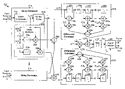
[0041] FIG. 5 shows an embodiment of first detection stage and timing
acquisition
unit 410, which performs signal detection using time-domain correlation. Unit
410
operates on complex-valued input samples at the sample rate, which is equal to
or
higher than the chip rate. For simplicity, the following description assumes
that the
input samples are provided at the chip rate. In the following description,
"tit" is an
index for receive antenna, "n" is an index for chip period, "k" is an index
for frequency
bin, and "i" is an index for the 128 bits in the fixed sequence sent in the
SYNC field.
The symbol rate is equal to the bit rate for the pilot sent in the SYNC field.
Coherent
sum refers to a sum of complex values, and non-coherent sum refers to a sum of
real
values (e.g., magnitudes).
[0042] Within unit 410, delay correlators 510a through 510r receive the input
samples from receiver units 154a through 154r, respectively. Within delay
correlator
510a for antenna 1 (or in =1), a Barker despreader 512a despreads the input
samples
with the 11-chip Barker sequence and provides despread symbols at the chip
rate. For
each chip period n, Barker despreader 512a multiplies 11 input samples for
chip periods
n through n -10 with the 11 chips of the Barker sequence, accumulates the
results of
the multiplication, and provides a despread symbol xm(n) for that chip period.
Barker
despreader 512a performs a sliding correlation of the Barker sequence with the
input
samples to obtain a despread symbol for each chip period (instead of each
symbol
period) and provides despread symbols to a symbol buffer 514a and a delay
multiplier
520a.
[0043] Delay multiplier 520a generates 1-symbol and 2-symbol delayed products
of
the despread symbols. Within delay multiplier 520a, the despread symbols are
provided
CA 02609423 2007-11-23
WO 2006/130502 PCT/US2006/020541
to two series-coupled delay units 522a and 522b, with each delay unit
providing a delay
of one symbol period T5, which is equal to 11 chip periods, or TS =11 = Tc.
Units 524a
and 524b provide the complex conjugate of the despread symbols from delay
units 522a
and 522b, respectively. A multiplier 526a multiplies the despread symbol for
each chip
period n with the output of unit 524a and provides a 1-symbol delayed product
Yl m (1a)
for that chip period. Similarly, a multiplier 526b multiplies the despread
symbol for
each chip period n with the output of unit 524b and provides a 2-symbol
delayed
product y2 m (n) for that chip period.
[0044] The delay correlator for each remaining antenna processes the input
samples
for that antenna in the manner described above for antenna 1. Each delay
correlator
provides 1-symbol delayed products yl=n, (n) and 2-symbol delayed products y2
,,, (n)
for an associated antenna in. For each chip period n, a summer 528a coherently
sums
the products Yl m (n) , for in =1, ..., R , from all R delay correlators 510a
through 510r
and provides a product y1(n) for that chip period. For each chip period n, a
summer
528b sums the products y2 m (n) , for in=1,...,R, from all delay correlators
510a
through 510r and provides a product y2 (n) for that chip period. The products
y1(n)
and y2(n) maybe expressed as:
R
Yl(fz) _ Ixm(n) xn(n-TS) ,and Eq (1a)
M=1
R
Y2(n)= Zxm(n)=xm(n-2T,) . Eq (ib)
m=1
[0045] The 1-symbol delayed product yl n, (n) is indicative of the phase
difference
between two despread symbols xm (n) and x,,, (n - Ts) that are separated by
one symbol
period for antenna in. The 2-symbol delayed product Y2,,,, (n) is indicative
of the phase
difference between two despread symbols x(n) and xm (n - 2T5) that are
separated by
two symbol periods for antenna in. FIG. 5 shows the use of 1-symbol and 2-
symbol
delayed products for signal detection. In general, products for any number of
different
delays (e.g., 1, 2, 3 symbol periods, and so on) may be used for signal
detection. Using
products for more delays may improve SNR and detection performance. However,
CA 02609423 2007-11-23
WO 2006/130502 PCT/US2006/020541
11
since frequency offset causes phase rotation in the input samples, the maximum
delay
may be limited by the frequency offset. The amount of delay also affects the
complexity of differential correlators 530a and 530b. For example, there are
127
multiply and accumulate operations for a delay of one symbol period, 126
multiply and
accumulate operations for a delay of two symbol periods, and so on.
[0046] Differential correlators 530a and 530b receive the products y1(n) and
y2 (n) , respectively. Within differential correlator 530a, the products y1(n)
are
provided to a sequence of alternating delay elements 532a and 534a. Each delay
element 532a provides a delay of one chip period, each delay element 534a
provides a
delay of 10 chip periods, each pair of adjacent delay elements 532a and 534a
provides a
delay of 11 chip periods (which is one symbol period), and the entire sequence
of delay
elements 532a and 534a provides a delay of approximately 126 symbol periods. A
set
of 127 adders 536a couples to the 127 delay elements 532a. Each adder 536a
sums the
input and output of an associated delay element 532a and provides an output
y1 (n -11 = i) = y1(n -11 = i -1) , where i E { 0, ..., 1261. A set of 127
multipliers 538a
couples to the set of 127 adders 536a and also receives a 1-symbol
differential sequence
containing 127 known values. This sequence is formed by a bit-wise product of
a first
sequence of do through d126 with a second sequence of d1 through d127, where
do through
d127 are the 128 bits of the fixed sequence (or pilot bits) used for the SYNC
field. Since
the pilot bits are real-valued, d;d,+1 = did;+1 for i E { 0, ..., 1261. Each
multiplier 538a
multiplies the output of an associated summer 536a with did,+1. For each chip
period fa,
an adder 540a adds the outputs from all 127 multipliers 538a and provides a
correlation
result cl (12) for that chip period.
[0047] Differential correlator 530b is similar to differential correlator
530a. The
products y2 (1t) are provided to a sequence of alternating delay elements 532b
and 534b
that provides a delay of approximately 125 symbol periods. A set of 126 adders
536b
couples to 126 delay elements 532b. Each adder 536b sums the input and output
of an
associated delay element 532b and provides an output y2 (ii -11 = i) = y2 (n -
11 = i -1),
where i E { 0, ..., 1251. A set of 126 multipliers 538b couples to the set of
126 adders
536b and also receives a 2-symbol differential sequence containing 126 known
values.
This sequence is formed by a bit-wise product of a sequence of do through d125
with a
sequence of d2 through d127. Each multiplier 538b multiplies the output of an
associated
CA 02609423 2007-11-23
WO 2006/130502 PCT/US2006/020541
12
summer 536b with d;di+2 . For each chip period n, an adder 540b adds the
outputs from
all 126 multipliers 538b and provides a correlation result c2(k) for that chip
period.
[0048] Differential correlator 530a performs correlation between the 1-symbol
delayed products yl (n) with the 1-symbol differential sequence. Differential
correlator
530b performs correlation between the 2-symbol delayed products y2 (n) with
the 2-
symbol differential sequence. The embodiment shown in FIG. 5 assumes that the
wireless channel has a delay spread (i.e., dispersion or smear) of a few
chips. Summers
536a and 536b are used to collect energy across this delay spread. The energy
may also
be collected over more chips for a larger delay spread, or may be omitted if
the wireless
channel has zero or very little delay spread (e.g., for a strong line-of-sight
path).
[0049] Each differential correlator 530 provides a correlation result for each
chip
period. The phases of the correlation results c2 (n) from differential
correlator 530b
may not be aligned with the phases of the corresponding correlation results cl
(n) from
differential correlator 530a. A multiplier 542 multiplies each correlation
result c2 (n)
from differential correlator 530b with a complex phasor e-' ' for L different
hypothesized phases and provides a set of L phase-rotated correlation results.
For
example, the hypothesized phases may be 10, 90 , 180 , -90 } for L = 4, 10, 60
,
- 60 } for L = 3, and so on. The L hypothesized phases may be selected to
cover the
possible range of relative phases. For example, the maximum frequency offset
may be
232 KHz for a frequency error of 20 ppm and a 5.8 GHz carrier frequency. The
maximum difference in phase between the 1-symbol and 2-symbol delayed
correlations
is 232 KHz times 1 s, which is approximately 90 degrees. Hence, if
hypothesized
phases of 0, 60 , and -60 are used, then least one hypothesized phase is
within 30 . If
the phase difference is larger (e.g., due to the use of a larger delay or a
larger frequency
offset), then the hypothesized phases should cover a larger range, up to the
full 180 .
[0050] Multiplier 542 rotates c2 (n) by different phases. For each chip period
n, an
adder 544 coherently adds the correlation result cl (n) from adder 540a with
each of the
L corresponding phase-rotated correlation results from multiplier 542 and
provides L
combined correlation results z, (n), for p =1, ..., L. If K differential
correlators are
used for K different delays, where K > 1, then one differential correlator may
be used as
the reference (with no phase shift). One combined correlation result is then
obtained for
CA 02609423 2007-11-23
WO 2006/130502 PCT/US2006/020541
13
each hypothesis corresponding to a specific phase for each of the K -1
remaining
differential correlators. For example, if K = 3, then one combined correlation
result is
obtained for each hypothesis corresponding to a different pair of hypothesized
phases
for two differential correlators. Up to LK-1 combined correlation results are
obtained
for the 0-1 possible hypotheses. For each chip period n, a unit 546 computes
the
squared magnitude of each of the L combined correlation results (for K = 2),
identifies
the largest squared magnitude value among the L squared magnitude values, and
provides this largest squared magnitude value Z(n). For each chip period n, a
signal
detector 548 compares the largest squared magnitude value Z(n) against a
predetermined threshold Zth and declares the presence of a PPDU if Z(n)
exceeds the
threshold, or Z(n) > Zt,, . Signal detector 548 continues to monitor the
squared
magnitude values to search for a peak value and provides the chip period for
this peak
value as an initial timing tau for the detected PPDU.
[0051] Alternatively, the correlation results c,(n) and c2(n) for each chip
period
may be non-coherently combined. This may be achieved by computing the squared
magnitude of c, (n) , computing the squared magnitude of c2 (n) , and summing
the two
squared magnitudes to obtain Z(n). The threshold Zth may be set to different
values
depending on how Z(n) is derived.
[0052] The threshold Zth used for the first detection stage may be an adaptive
threshold that varies, e.g., with the received energy Erx for the 128-bit SYNC
field. For
example, the threshold Zth may be set equal to the received energy Erx times a
scaling
factor S1, or Z. = E,.x = S, . The use of normalized received energy for
signal detection
results in similar detection performance for a wide range of received signal
levels.
Computer simulation indicates that a detection probability of approximately
90% and a
false alarm rate of less than 1% may be achieved for a 2 equal-path
uncorrelated
Rayleigh channel at a total SNR of -3 dB using S, = 22. Detection probability
refers to
the likelihood of correctly declaring the presence of a PPDU when the PPDU is
sent.
False = alarm rate refers to the likelihood of erroneously declaring the
presence of a
PPDU when none is sent. A tradeoff between detection probability versus false
alarm
rate may be made by selecting a suitable value for the scaling factor S1.
[0053] FIG. 6 shows an embodiment of second detection stage and frequency
acquisition unit 420, which performs signal detection using frequency-domain
CA 02609423 2007-11-23
WO 2006/130502 PCT/US2006/020541
14
processing. For this embodiment, unit 420 includes R frequency offset
estimators 610a
through 610r for the R receive antennas. Each frequency offset estimator
detects the
energies in different frequency bins to determine the frequency offset in the
input
samples from an associated antenna.
[0054] For receive antenna 1 (in =1), symbol buffer 516a provides N despread
symbols that are spaced apart by 11 chip periods (or one symbol period)
starting at the
initial timing tau provided by timing acquisition unit 410. The first despread
symbol is
thus time-aligned with the best timing hypothesis from the timing acquisition
stage. In
general, N may be any integer that is a power of two and does not exceed 128,
e.g., N
may be 32, 64, or 128. Within frequency offset estimator 610a, a set of N
multipliers
612 receives the N despread symbols from symbol buffer 514a and N
corresponding
pilot bits in the 128-bit sequence. Each multiplier 612 multiplies its
despread symbol
with its pilot bit to remove the modulation on that despread symbol. An N-
point fast
Fourier transform (FFT) unit 620 receives the N outputs from N multipliers
612,
performs an N-point FFT on these N outputs, and provides N frequency-domain
values
for N frequency bins. A set of N units 622 receives the N frequency-domain
values
from FFT unit 620. Each unit 622 computes the squared magnitude of its
frequency-
domain value and provides the detected energy for a respective frequency bin
k.
[0055] After removing the modulation with multipliers 612, the N outputs from
these multipliers may have a periodic component. This periodic component is
caused
by a frequency offset in the oscillator at receiving station 150, which
results in the
received signal not being frequency downconverted exactly to DC. FFT unit 620
provides a spectral response of the N outputs from multipliers 612. The
frequency bin k
with the largest detected energy is indicative of the frequency offset for the
input
samples from antenna in.
[0056] The frequency offset estimator for each remaining receive antenna
processes
the despread symbols for that antenna in the manner described for antenna 1. A
set of N
adders 632 receives R sets of N detected energies from R frequency offset
estimators
610a through 610r for the R receive antennas. Each adder 632 adds the detected
energies from all R frequency offset estimators 610a through 610r for an
associated
frequency bin k and provides the total detected energy E(k) for that frequency
bin. A
selector 634 selects the largest total detected energy E.X (k) among the N
total detected
energies for the N frequency bins. A signal detector 636 compares the largest
total
CA 02609423 2007-11-23
WO 2006/130502 PCT/US2006/020541
detected energy E,,,aX (k) against a predetermined threshold Eth, declares
signal detection
if E., (k) is greater than the threshold Eth, and provides the frequency bin
with the
largest total detected energy as the estimated frequency error k0 . The
threshold Eth may
be set equal to, e.g., the received energy Erx for the 128-bit SYNC field
times a scaling
factor S2, or E. = Eõ, = S2 .
[0057] The embodiment shown in FIG. 6 utilizes an N-point FFT, where N< 128.
If N = 64, which is the FFT size commonly used for 802.1lb and 802.11g for
OFDM,
then the spacing between adjacent frequency bins is 15.625 KHz for the 1 Msps
symbol
rate, and the uncertainty in the frequency offset estimate is half of the bin
spacing or
7.812 KHz. This uncertainty may be reduced by performing interpolation and/or
using
a larger 128-point FFT.
[0058] The processing gain for coherent accumulation by the FFT is
approximately
18 dB for N = 64. The worst-case coherent integration loss is nearly 4 dB,
which
occurs when the actual frequency offset is exactly between two frequency bins.
A
minimum total integrated SNR of almost 14 dB may be achieved for N = 64. Most
of
the coherent integration loss may be recovered by summing the detected
energies for
pairs of adjacent frequency bins (e.g., similar to the summing performed by
adders 536a
and 536b in FIG. 5) prior to selecting the largest total detected energy.
Summing the
detected energies for adjacent frequency bin pairs improves the detection
probability at
a cost of a small increase in the false alarm rate. A detection probability of
better than
90 % at an SNR of -7 dB and better than 99.9 % at an SNR of -4 dB may be
achieved
using a threshold of S2 = 8. The false alarm probability is less than 0.5 %
for the
second detection stage, yielding an aggregate false alarm rate of 5x10"5 for
both the first
and second detection stages.
[0059] Multipath may degrade the detection probability since all of the energy
is not
used in the second detection stage (due to the FFT operating at the symbol
spacing
instead of chip spacing). In an embodiment, improved detection performance may
be
achieved for the second detection stage by performing a 128-point FFT and
hence
integrating over the entire 128-bit sequence for the SYNC field. In another
embodiment, one 64-point FFT may be performed for the first half of the 128-
bit
sequence as described above, another 64-point FFT may be performed for the
second
half of the 128-bit sequence, and the detected energies for the two FFTs may
be non-
coherently summed by adders 632.
CA 02609423 2007-11-23
WO 2006/130502 PCT/US2006/020541
16
[0060] In another embodiment of frequency offset estimation, the input samples
are
correlated with the known 128-bit sequence for different hypothesized
frequency
offsets. For each hypothesized frequency offset, the input samples are rotated
by that
frequency offset, the rotated samples are correlated with the 128-bit
sequence, the
correlation result is compared against a threshold, and signal detection is
declared if the
correlation result exceeds the threshold. The correlation may be performed in
the time
domain with a finite impulse response (FIR) filter structure or in the
frequency domain
with an FFT-multiply-IFFT operation. The frequency offset estimate is
determined by
the hypothesized frequency error that yields the largest correlation result
exceeding the
threshold.
[0061] In yet another embodiment of frequency offset estimation, the input
samples
are initially despread to obtain despread symbols at chip rate, as shown in
FIG. 5. The
despread symbols are then multiplied with the corresponding pilot bits to
remove the
pilot modulation. The resultant symbols are used to generate 1-symbol and 2-
symbol
delayed products, e.g., using delay multiplier 520a in FIG. 5. The delayed
products for
each delay are processed to generate a complex value for that delay. For each
delay d,
where d =I 1, 21, the d-symbol delayed products are provided to a set of 10
series-
coupled chip-spaced delay elements (e.g., similar to delay elements 722 in
FIG. 7) to
obtain d-symbol delayed products at 11 different chip offsets. The d-symbol
delayed
products for each chip offset is coherently accumulated across the SYNC field
(e.g.,
using switches 724 and accumulators 730 in FIG. 7). The 11 accumulated results
for
the 11 chip offsets may be combined (e.g., using maximal ratio combining) to
generate
a complex value Vd for delay d. The phase difference between the complex
values Vl
and V2 for 1-symbol and 2-symbol delays may be computed and used to derive the
frequency offset. The R receive antennas may be combined in various manners,
e.g.,
the delayed products may be combined across antennas as shown in FIG. 5, the
complex
values for different antennas may be combined for each delay d, and so on.
More than
two delays and/or a larger delay may also be used for frequency estimation. A
larger
delay results in a larger phase difference, which provides better resolution
for the
frequency offset. However, a larger delay may result in ambiguity, e.g., a
phase shift of
more than 180 may be interpreted as a negative shift of less than 180 . For a
given the
number of delays and a given maximum frequency offset, a set of delays may be
selected to optimize resolution without ambiguity.
CA 02609423 2007-11-23
WO 2006/130502 PCT/US2006/020541
17
[0062] Regardless of the technique used for frequency estimation, the
estimated
frequency offset k0S from frequency acquisition unit 420 typically contains
residual
frequency error. To estimate this residual frequency error, a first 11-tap
channel
estimate may be derived based on the first 64 bits of the SYNC field (e.g., as
described
below), a second 11-tap channel estimate may be derived based on the last 64
bits of the
SYNC field, with both channel estimates being derived with the frequency
offset k0
removed. The product of the second channel estimate and the complex conjugate
of the
first channel estimate may be computed, on a per tap basis. The 11 resultant
products
may be coherently summed to obtain the phase difference between the two
channel
estimates. Thresholding may be performed on (1) each channel tap prior to
computing
the product and/or (2) each product prior to summing the products. The
thresholding
removes channel taps with low energy below a predetermined threshold. The
residual
frequency error may be estimated based on the phase difference between the two
channel estimates and may be provided to filter 452 and/or frequency
correction unit
454 and used to correct the timing and/or the frequency of the input samples
(not shown
in FIG. 4). This updating of the frequency offset koS with the residual
frequency error
estimate may improve demodulation performance.
[0063] FIG. 7 shows an embodiment of third detection stage and channel
estimation
unit 430, which performs signal detection using time-domain processing. For
this
embodiment, unit 430 includes R channel estimators 710a through 710r for the R
receive antennas. Each channel estimator may derive a channel impulse response
estimate containing channel taps that are spaced at the sample rate. For
example, up to
11 channel taps spaced by one chip may be obtained if despread symbols are
obtained at
the chip rate, up to 22 channel taps spaced by half chip may be obtained if
despread
symbols are obtained at the twice the chip rate (or chipx2), and so on. For
the
embodiment shown in FIG. 7, each channel estimator derives an 11-tap channel
impulse
response estimate at chip spacing for an associated antenna.
[0064] Within channel estimator 710a for antenna 1 (m =1), a multiplier 712
multiplies the despread symbols for antenna m with a complex phasor e-' =T to
remove the frequency error k,,, determined by frequency acquisition unit 420.
Multiplier
712 provides frequency-corrected symbols at the chip rate to a set of 10
series-coupled
delay elements 722. Each delay element 722 provides a delay of one chip
period. A set
of 11 switches 724 couples to the output of multiplier 712 and the outputs of
the 10
delay elements 722. Switches 724 are enabled for one chip period in each
symbol
CA 02609423 2007-11-23
WO 2006/130502 PCT/US2006/020541
18
period and provide 11 frequency-corrected symbols for that symbol period. The
control
signal for switches 724 is determined by the initial timing tau from timing
acquisition
unit 410 and is generated such that the frequency-corrected symbol from the
fifth delay
element 722 (which is for the center tap of an 11-tap channel impulse response
estimate)
corresponds to the best timing hypothesis provided by the timing acquisition
stage.
[0065] Channel estimation is performed over a predetermined time window W,
which is selected to achieve adequate SNR or quality for the channel
estimates. The
time window W may be M symbol periods long, where M may be, e.g., M > 31. A
set
of 11 multipliers 726 receives the pilot bit dl for each symbol period in
which channel
estimation is performed. Each multiplier 726 multiplies the output of a
respective
switch 724 with the pilot bit di, removes the modulation by the pilot bit, and
provides its
output to a respective accumulator 730. The set of 11 accumulators 730 is
reset at the
start of the channel estimation. Each accumulator 730 coherently accumulates
the
output of a respective multiplier 726 over the time window W. A set of 11
switches 732
couples to the set of 11 accumulators 730. Switches 732 are enabled at the end
of the
time window W and provide the 11 channel taps h. ,O through h,,,,10 for the
channel
impulse response estimate for antenna in. This channel estimate may be used
for data
demodulation, as described below. A set of 11 units 734 receives the 11
channel taps,
and each unit 734 computes a squared magnitude of its channel tap. A summer
736
sums the outputs from all 11 units 734 and provides the total energy for all
channel taps
for antenna in. Alternatively, the output of each unit 734 may be compared
against a
threshold value, and summer 736 may sum only the outputs that exceed the
threshold
value. The threshold value may be set to a predetermined percentage of the
total energy
for all 11 channel taps.
[0066] The channel estimator for each remaining receive antenna processes the
despread symbols for that antenna in the manner described above for antenna 1.
A
summer 738 sums the total energies from all R channel estimators 710a through
710r
and provides the total energy H for all R antennas. A signal detector 740
compares the
total energy H against a predetermined threshold Hth and declares signal
detection if H
exceeds the threshold Hth. The threshold Hth may be set equal to, e.g., the
received
energy Erx for the 128-bit SYNC field times a scaling factor S3, or Hth = E,.x
= S3 .
[0067] A detection probability of better than 99 % and a false alarm rate of
less than
10-5 may be achieved at an SNR of -4 dB using a threshold of S3 =14 . An
aggregate
CA 02609423 2007-11-23
WO 2006/130502 PCT/US2006/020541
19
false alarm rate of less than 10-9 may be achieved with all three detection
stages. This
assumes that the three detection stages are uncorrelated because different
types of signal
processing are used for the three stages.
[0068] For the embodiments described above, signal detection may be achieved
based on time-domain correlation (FIG. 5), frequency-domain processing (FIG.
6), and
time-domain processing (FIG. 7). All three types of signal processing may be
used to
provide good detection performance (e.g., a high detection probability and a
low false
alarm rate) for poor channel conditions (e.g., a low SNR). Any combination of
signal
processing may also be used for signal detection.
[0069] FIGS. 5, 6 and 7 show specific embodiments of signal detection, timing
acquisition, frequency acquisition, and channel estimation, which may be
performed in
other manners. For example, signal detection and timing acquisition may be
performed
with just 1-bit delayed differential correlator 530a. A combination of
techniques may
also be used. For example, the input samples may be rotated for few (e.g.,
two)
hypothesized frequency offsets. The residual frequency error is smaller for
one of the
hypothesized frequency offsets, so the Barker despreading (or coherent
accumulation)
may be performed over a longer duration (e.g., 22 chips). The despread symbols
from
the longer coherent accumulation may be provided to the delay multiplier and
differential correlator shown in FIG. 5. Signal detection may be achieved for
a lower
operating SNR since coherent accumulation is performed over a longer duration.
[0070] FIGS. 5, 6 and 7 show exemplary signal processing by units 410, 420 and
430, respectively. The processing may be implemented in various manners using
hardware, software, and/or firmware. For example, units 410, 420 and 430 may
be
implemented with dedicated hardware or may share hardware. A digital signal
processor (DSP) and/or some other type of processor may perform the processing
for
units 410, 420 and 430 in a time division multiplexed manner. Sample buffer
402,
symbol buffer 514, and/or some other buffer may be used to buffer data for
processing.
[0071] Referring back to FIG. 4, once a PPDU has been detected, a
determination is
made whether the received PPDU is for 802.llb/g or the range extension mode,
e.g.,
based on the PLCP preamble and/or PLCP header. A DSSS receive processor 440
processes the received PPDU if it is for 802.11b/g. A DSSS receive processor
450
processes the received PPDU if it is for the range extension mode.
[0072] DSSS receive processor 440 performs spectral despreading and
demodulation for 802.1 lb/g. Within processor 440, a rake receiver/equalizer
442
CA 02609423 2007-11-23
WO 2006/130502 PCT/US2006/020541
despreads the input samples with the Barker sequence, equalizes the despread
symbols
based on the channel estimates, combines signal components across the R
receive
antennas, and provides detected symbols. A demodulator (Demod) 444 demaps the
detected symbols based on the modulation scheme (e.g., BPSK or QPSK) used for
transmission, performs differential decoding, and provides output bits, which
are
estimates of the data bits sent by transmitting station 110.
[0073] DSSS receive processor 450 performs spectral despreading, demodulation,
and FEC decoding for the range extension mode. Within processor 450, a filter
452
filters the input samples for each receive antenna to remove out-of-band noise
and
interference. Filter 452 may also resample the input samples for each receive
antenna
(1) for sample rate conversion from the sampling rate to the chip rate and/or
(2) to
compensate for timing drift across the received PPDU. For 801.11g, the input
samples
are typically at multiple times the OFDM chip rate of 20 MHz. In this case,
filter 452
may perform resampling from multiple times 20 MHz to either 11 MHz for a chip-
spaced rake receiver or 22 MHz for a half chip-spaced rake receiver. The local
oscillator (LO) signal used for frequency downconversion and the sampling
clock used
to generate the input samples are typically derived from the same reference
oscillator.
In this case, the frequency error in the sampling clock may be determined
based on the
frequency error k0 determined by frequency acquisition unit 420 for the LO
signal. The
timing drift in the input samples may then be determined based on the
frequency offset
k0s and the carrier frequency. Filter 452 may make periodic adjustment of
Tadj based
on the frequency offset k0 , where Tadj may be a fraction of a sample period.
[0074] In an embodiment, filter 452 is implemented as a polyphase filter
composed
of a bank of N base filters, where N > 1. Each base filter is associated with
a specific
set of coefficients for a specific time offset. In an exemplary design, filter
452 includes
11 FIR filters, with each FIR filter having four taps. A different base filter
may be used
to produce each successive output sample. If the frequency offset is zero,
then the 11
base filters may be cycled through in a fixed order, with every 11-th sample
coming
from the same base filter. In order to compensate for timing drift, a given
base filter
may be skipped and the next base filter may be used instead, or the same base
filter may
be used for two successive output samples. Timing adjustment may thus be
achieved by
selecting an appropriate base filter in use.
[0075] A frequency correction unit 454 removes the frequency offset in the
timing-
adjusted samples for each receive antenna. Unit 454 may be implemented with a
CA 02609423 2007-11-23
WO 2006/130502 PCT/US2006/020541
21
numerically controlled oscillator (NCO) and a complex multiplier, similar to
multiplier
712 in FIG. 7. The NCO generates a phasor rotating at the offset frequency k0
provided
by frequency acquisition unit 420. The multiplier multiplies the timing-
adjusted
samples for each receive antenna with the phasor and provides frequency-
corrected
samples for that antenna.
[0076] A rake receiver/despreader 456 performs coherent detection of the
frequency-corrected samples with the channel estimates and combines signal
components across receive antennas and multipaths. Rake receiver 456
multiplies the
frequency-corrected samples for each receive antenna with the 11 channel taps
provided
by channel estimation unit 430 for that antenna. Rake receiver/despreader 456
also
performs despreading with the Barker sequence, accumulates the despread
symbols for
all R antennas, and provides detected symbols. In an embodiment, the channel
estimates for the R receive antennas are derived once based on the SYNC field
and
possibly other fields of the received PPDU, and these channel estimates are
used for the
entire received PPDU. For this embodiment, rake receiver 456 is not tracking
the
wireless channel across the received PPDU. In another embodiment, the channel
estimates are updated using hard decisions obtained from the detected symbols
and/or
decisions obtained by re-encoding and re-mapping the output of an FEC decoder
464.
[0077] A phase correction unit 458 removes phase error in the detected
symbols.
The phase error is due to a residual frequency error that results from
receiver 160 not
being phase-locked.
[0078] FIG. 8 shows a block diagram of an embodiment of phase correction unit
458. Within unit 458, a multiplier 812 rotates each detected symbol from rake
receiver
456 by a phase reference 0,ef (t) and provides a corresponding phase-corrected
symbol.
A unit 814 generates a hard decision (e.g., +1 or -1) for each phase-corrected
symbol.
A multiplier 816 multiplies each detected symbol with the corresponding hard
decision
and provides a product for that detected symbol. A unit 818 computes a moving
average of the products from multiplier 816 and provides an averaged product.
For
each symbol period, a unit 820 normalizes and conjugates the averaged product
and
provides the phase reference ,ef (t) for the detected symbol for that symbol
period t.
The phase reference may thus be derived by averaging over a window of detected
symbols. The averaging may be designed to account for the fact that the phase
information from the known pilot symbols in the SYNC field is more reliable
but may
CA 02609423 2007-11-23
WO 2006/130502 PCT/US2006/020541
22
not be current whereas the phase information for the detected symbols may not
be as
reliable but is more current.
[0079] Referring back to FIG. 4, a demodulator 460 performs coherent
demodulation of the phase-corrected symbols. For BPSK, demodulator 460 may
provide the real component of each phase-corrected symbol a demodulated
symbol,
which is an estimate of the data symbol sent by transmitting station 110. For
other
modulation schemes, demodulator 460 may provide a modulation symbol that is
most
likely to have been sent for each phase-corrected symbol as a demodulated
symbol.
[0080] A deinterleaver 462 deinterleaves the demodulated symbols in a manner
complementary to the interleaving performed by interleaver 256 in FIG. 2. FEC
decoder 464 decodes the deinterleaved symbols in a manner complementary to the
encoding performed by FEC encoder 252 in FIG. 2 and provides output data. A
multiplexer 470 receives the output data from DSSS receive processors 440 and
450,
provides the output data from DSSS receive processor 440 if the received PPDU
is for
802.11b/g, and provides the output data from DSSS receive processor 450 if the
received PPDU is for the range extension mode.
[0081] FIG. 4 shows a specific embodiment of receive processor 160 for
802.11b/g
and the range extension mode. Receive processor 160 may also be implemented
with
other designs, and this is within the scope of the invention. In general, the
processing
by DSSS receive processor 440 is complementary to the processing by DSSS
transmit
processor 240 at transmitting station 110, and the processing by DSSS receive
processor
450 is complementary to the processing by DSSS transmit processor 250. FIG. 4
shows
exemplary designs of DSSS receive processors 440 and 450, which may include
other
and/or different processing units not shown in FIG. 4.
[0082] FIG. 9 shows a process 900 for performing signal detection for the
first
stage. Input samples are despread with a code sequence to generate despread
symbols,
e.g., at chip rate (block 912). Products of despread symbols are generated for
at least
two different delays (block 914). Each product is generated based on a
despread
symbol and a complex conjugate of another despread symbol that is at least one
symbol
period earlier. For example, 1-symbol delayed products and 2-symbol delayed
products
may be generated as shown in FIG. 5, with each 1-symbol delayed product being
generated with two despread symbols that are separated by one symbol period,
and each
2-symbol delayed product being generated with two despread symbols that are
separated by two symbol periods.
CA 02609423 2007-11-23
WO 2006/130502 PCT/US2006/020541
23
[0083] Correlation between the products for each delay and the known values
for
that delay is then performed (block 916). The known values may be products of
pilot
bits, as shown in FIG. 5. Adjacent products for each delay may be summed prior
to
performing correlation to account for delay spread in the wireless channel, as
also
shown in FIG. 5. Correlation results for all of the delays are combined (block
918).
The correlation results for the 2-symbol delay may be rotated by multiple
hypothesized
phases and combined with the corresponding correlation results for the 1-
symbol delay,
and the combined correlation results with the largest magnitude among the
multiple
hypothesized phases may be selected, as shown in FIG. 5. Alternatively, the
correlation
results for the different delays may be non-coherently combined.
[0084] The presence of a signal/transmission is then detected based on the
combined correlation results, e.g., by comparing the combined correlation
results
against an adaptive threshold Zth that is a function of the received energy
(block 920).
The timing of the signal is also determined based on the combined correlation
results,
e.g., by detecting for a peak in the combined correlation results (block 922).
[0085] FIG. 10 shows a process 1000 for performing signal detection with
multiple
(e.g., three) stages using different types of signal processing. Adaptive
thresholds used
for signal detection by the stages are derived based on the received energy
for a window
of symbols (block 1012). Signal detection for the first stage is performed
using time-
domain correlation and a first threshold (block 1014). For the first stage,
products of
symbols may be generated for at least one delay, correlation between the
products for
each delay and known values for that delay may be performed, and detection may
be
declared based on the correlation results for the at least one delay and the
first threshold.
Signal detection for a second stage is performed using frequency-domain
processing
and a second threshold (block 1016). For the second stage, energies for
multiple
frequency bins may be determined, and detection may be declared based on the
energies
for these frequency bins and the second threshold. Signal detection for a
third stage is
performed using time-domain processing and a third threshold (block 1018).
Multiple
channel taps for a channel impulse response estimate may be derived, and
detection may
be declared based on the channel taps and the third threshold. The presence of
a signal
is declared based on the outputs of the first, second and third stages (block
1020).
[0086] FIG. 11 shows a process 1100 for receiving a transmission or PPDU. The
timing of input samples is adjusted to obtain timing-adjusted samples (block
1112). The
timing adjustment may be performed with a polyphase filter and/or based on a
CA 02609423 2007-11-23
WO 2006/130502 PCT/US2006/020541
24
frequency offset determined during frequency acquisition. The frequency offset
in the
timing-adjusted samples is removed to obtain frequency-corrected samples
(block
1114). The frequency-corrected samples are processed with a channel estimate
(e.g.,
using a rake receiver) to obtain detected symbols (block 1116). The phases of
the
detected symbols are corrected to obtain phase-corrected symbols (block 1118).
For the
phase correction, a phase reference may be derived based on the detected
symbols, and
the phases of the detected symbols may be corrected based on the phase
reference.
Demodulation is performed on the phase-corrected symbols to obtain demodulated
symbols (block 1120). The demodulated symbols are deinterleaved (block 1122),
and
the deinterleaved symbols are decoded to obtain decoded data (block 1124).
[0087] The processes depicted and described with respect to Figs. 9-11 may be
implemented as functions performed by processor 160. The individual blocks may
comprise instructions that are performed by processor 160.
[0088] The techniques described herein may be implemented by various means.
For
example, these techniques may be implemented in hardware, firmware, software,
or a
combination thereof. For a hardware implementation, the processing units used
to
perform signal detection, acquisition, and demodulation may be implemented
within
one or more application specific integrated circuits (ASICs), digital signal
processors
(DSPs), digital signal processing devices (DSPDs), programmable logic devices
(PLDs), field programmable gate arrays (FPGAs), processors, controllers, micro-
controllers, microprocessors, electronic devices, other electronic units
designed to
perform the functions described herein, or a combination thereof.
[0089] For a software implementation, the techniques may be implemented with
modules (e.g., procedures, functions, and so on) that perform the functions
described
herein. The software codes may be stored in a memory unit (e.g., memory unit
182 in
FIG. 1) and executed by a processor (e.g., processor 160 and/or processor
180). The
memory unit may be implemented within the processor or external to the
processor.
[0090] The previous description of the disclosed embodiments is provided to
enable
any person skilled in the art to make or use the present invention. Various
modifications to these embodiments will be readily apparent to those skilled
in the art,
and the generic principles defined herein may be applied to other embodiments
without
departing from the spirit or scope of the invention. Thus, the present
invention is not
intended to be limited to the embodiments shown herein but is to be accorded
the widest
scope consistent with the principles and novel features disclosed herein.